Overlapping domains for topology optimization of large-area metasurfaces
Abstract
We introduce an overlapping-domain approach to large-area metasurface design, in which each simulated domain consists of a unit cell and overlapping regions from the neighboring cells plus PML absorbers. We show that our approach generates greatly improved metalens quality compared to designs produced using a locally periodic approximation, thanks to better accuracy with similar computational cost. We use the new approach with topology optimization to design large-area () high-NA (0.71) multichrome and broadband achromatic lenses with high focusing efficiency (), greatly improving upon previously reported works.
1 Introduction
Inverse-design techniques [1, 2, 3, 4, 5, 6, 7] have received increasing attention as a powerful approach for the design of optical metasurfaces (surfaces with aperiodic subwavelength patterns designed for free-space wavefront engineering) [8, 9, 10, 11, 12, 13, 14, 15, 16, 17, 18]. For example, with freeform topology optimization [19, 20], the resulting devices showed enhanced functionalities such as angular phase control [2] or large-angle beam deflection [1]. However, early designs were limited to small devices, whereas many practical applications require diameters [8] that would require enormous computational resources for full Maxwell simulations. More recently, new inverse-design techniques have become capable of large-area design, using either an interpolated library of offline simulation results for a few parameters [3] or freeform topology optimization (in which every “pixel” is a degree of freedom) with online Maxwell solvers [5]. The fundamental strategy to rapidly model a large-area metasurface is to divide it up into many unit cells and then simulate each cell independently. The set of simulated near-fields gathered from each cell are then “stitched together” (using the equivalence principle [3]) to approximate the total electromagnetic field anywhere above the surface. The key question is what to choose for the boundary conditions of these unit cells. One common choice is a Bloch-periodic boundary condition [9, 10, 11, 12, 13, 14, 15, 16], which corresponds to a locally periodic approximation (LPA) [3]. While LPA has proven to work well for monochromatic or small numerical-aperture (NA) metasurface designs[8, 9, 10, 11, 12, 13, 14, 15, 16, 17, 18, 3], it might not be suitable for designs which require more rapid variations in the dielectric structure, such as a high-NA multi-chrome metalens [5, 6].
Here, we introduce a new approach, called an overlapping-domain approximation (ODA), which is more accurate than LPA for topology-optimized metalens design with similar computational efficiency, and is inspired by domain-decomposition iterative solvers [21] but omits the iteration. In this approach, instead of sharply divided boundaries, each simulation domain contains the corresponding unit cell and some spatial overlap regions from the neighboring unit cells. Fig. 1 shows a schematic of our approach, in which an arbitrary aperiodic metasurface is divided into unit cells of size (two of which are shaded in Fig. 1), but the simulated domains have size with overlapping regions from the neighboring unit cells. The simulations are additionally padded by absorbing boundaries such as perfectly matched layers (PML) [22] instead of Bloch-periodic boundaries. From each simulated domain, we discard the electromagnetic field data in the overlapping regions: the fields in the size- unit cells are used to construct approximate fields anywhere above the surface similar to previous work [5]. Here, the motivation for PML is that applications such as lenses and beam-forming typically do not involve long-range light-propagation within the surface, so the suppression of such inter-cell scattering by the PML is appropriate (and superior to artificially periodic or Dirichlet boundaries) as long as is sufficiently large. In fact, we find that the introduction of PML reduces much of the LPA error (an observation also made by a recent work [7]) and that the error continues to fall with increasing overlap; overlap is especially crucial for situations with strong near-field inter-cell coupling. In particular, we find that is enough for accurate modeling of many lens designs. (In contrast, there will be other applications such as grating couplers or excitation of surface resonances [23] in which long-range surface propagation is crucial, but such propagation implies a nearly periodic surface in which LPA will be accurate. In this sense, ODA and LPA are complementary.) Not only do we demonstrate ODA’s improved accuracy over LPA (Sec. 2), but we also combine it with topology optimization [19, 20] to design large-area () high-NA (0.71) multi-chrome (red-green-blue/RGB, in Sec. 3) and broadband achromatic lenses (in Sec. 4) with high focusing efficiency (), greatly improving upon reported results in previous works [3, 5].

ODA is directly inspired by domain-decomposition techniques such as the Schwarz algorithm [24, 25, 26, 21, 27, 28]. These are iterative methods to find the exact solution of a large problem by repeatedly solving small problems in overlapping domains, where the boundary conditions of each domain are updated from its neighbors in the subsequent iteration. More generally, the solution of subproblems in small domains can be used as a preconditioner for many different iterative methods in linear algebra [29], and in such contexts some authors have even used overlapping domains with PML [30, 31]. From this perspective, ODA is simply the initialization step (or the 0th-order iteration) of a Schwarz-like algorithm, but the key observation is that this 0th-order approximation is sufficiently accurate for many metasurface design problems. Additional Schwarz iterations or similar schemes could be used for arbitrarily improved accuracy (or error estimates), but during metasurface optimization it is more important to solve the problem quickly than it is to solve it exactly, since the solution only needs to be good enough to point the optimization algorithm at an improved design for the next optimization step. More accurate simulations can be used at the end of the design process for validation; in this paper, we validate using brute-force finite-difference time-domain (FDTD) [32] simulations.
2 Locally periodic vs. overlapping-domain approximations
Fig. 2(a–c) demonstrates the limitations of LPA for a multi-chrome high-NA metalens design at RGB wavelengths (). The metalens consists of two layers of TiO2 (refractive index at RGB), each thick and separated by ; the lower layer is buried in silica (). The lens has a width and an NA of 0.71 and is designed by topology optimization under the locally periodic approximation (LPA) with the basic unit cell size, , using the approach described in Ref. [5]. The intensities are measured at the focal distance. The black lines denote LPA predictions while the red, green and blue lines denote rigorous full-wave FDTD simulations [32] of the entire metalens at the respective wavelengths, showing significant discrepancies between the two: rigorous simulations exhibit noisy side lobes while LPA predicts a relatively clean Airy [33] profile. It is worth noting that the overly optimistic results predicted by LPA indicate that topology optimization did manage to produce an optimal design which works well under LPA, but that the design contain rapid structural variations that violate the slowly-varying assumption behind LPA. Since the discrepancies between LPA and FDTD are apparently more pronounced for the red wavelength (Fig. 2a inset), we proceed to examine this case more closely. In particular, the error in the far-field intensities, defined as where is integrated over the focal plane, is as much as 17% under LPA (). In contrast, Fig. 2(d) shows that the error dramatically falls once we introduce the PML-termination even without any overlap (an observation also made by a recent work [7]) and continues to fall with overlapping domains () as described above, and in fact only suffices to lower the error by about a factor of 5 relative to LPA. This is also shown by Fig. 2(e), which reveals that ODA yeilds much better agreement with rigorous FDTD simulations. We expect that an overlap region will become even more important in metasurfaces with features that touch or cross unit-cell boundaries, especially for metallic structures that might exhibit strong near-field coupling between adjacent unit cells.
The introduction of PML combined with only a small overlap of lowers the error to a few percent or less in this structure, which requires only a modest increase in the computational cost of the subdomain simulations. The basic reason for this is that, in a metalens where light propagates mainly through (rather than along) the surface, the biggest effect of neighboring cells arises from the near fields of adjacent structures. We expect that larger overlapping regions may prove beneficial for taking into account stronger inter-cell scattering effects such as those found in higher dielectrics and plasmonic structures. Of course, there are also small corrections due to in-plane scattering from far-away cells, which leads to an error that decays extremely slowly with for . If one wished to correct for such small long-range errors, it would be more efficient to perform Schwarz (or similar) domain-decomposition iteration [21] rather than to increase the overlap . However, the agreement in Fig. 2(e) is already much better than has typically been used for metasurface designs in past work.
3 Topology optimization with overlapping domains
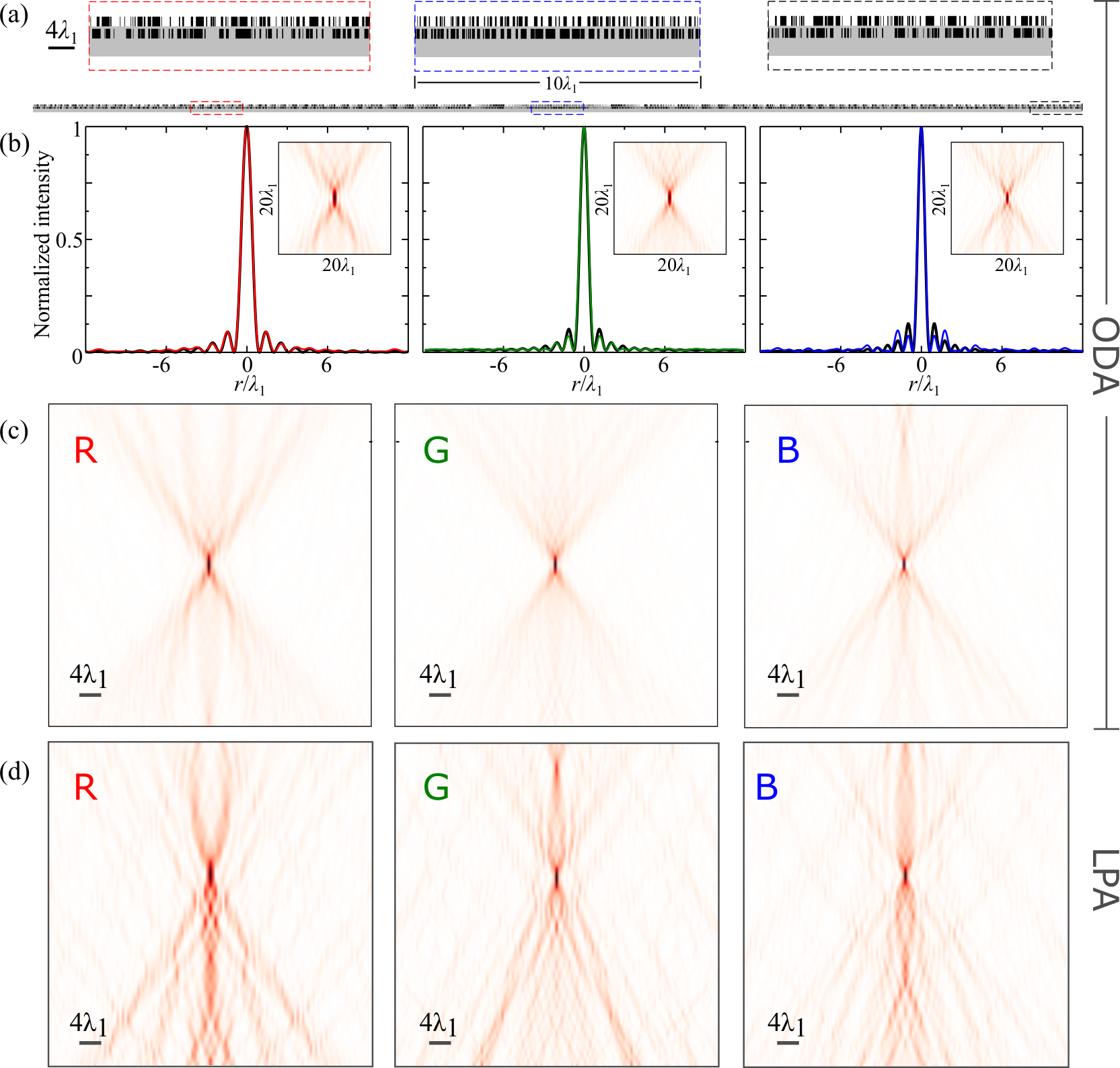
Encouraged by the error reduction observed in the previous section under ODA, we proceed to perform an ODA-based topology optimization for a metalens with the same dimensions, material parameters and target wavelengths as above. In particular, the optimization involves degrees of freedom (DOF) trying to maximize the minimum of focal intensities [5] at three different wavelengths (). Fig. 3(a) shows the binarized [19] topology-optimized ODA design with . The normalized far-field intensity profiles at the focal distance, Fig. 3(b), show that the metalens (colored lines) is performing virtually as well as a monochromatic lens (black lines) of the same NA at the corresponding wavelength. All three focal spots are diffraction-limited and the focusing efficiencies (defined as the fraction of incident power focused within a radius of 3 FWHM from the focal spot; FWHM = full width at half-maximum) around the focal spot divided by the total incident flux [34]) are found to be 45%, 48%, and 35% respectively. The field profiles in Fig. 3 are computed by full FDTD simulations (ODA is only used during optimization), but we find that ODA produces nearly indistinguishable results ( error). The superior performance of ODA is even more dramatically demonstrated by comparing Fig. 3(c) to a metalens optimized using LPA shown in Fig. 3(d): the latter (again, in full FDTD simulations performed after optimization) exhibits undesirable noise and parasitic focal points in the far field [5]. To the best of our knowledge, although high-NA achromatic metalenses with much smaller device sizes have been proposed [35], our design is the first multi-chrome (RGB) high-NA metalens to achieve good focusing performance over a large device size: for comparison, in Table 1, we have compiled a few of the most recent achromatic metalens designs reported to date. As noted in Ref. [35], it is extremely challenging to achieve a high-efficiency design over a broad bandwidth, a large diameter, and a high numerical aperture all simultaneously; our results show that an appropriately formulated topology-optimization framework combined with a vastly expanded design space can successfully address such issues. Although our proof-of-concept results are in two dimensions, we have shown that similar techniques scale to full 3d designs [5].
| NA | Diameter | 2d or 3d | Bandwidth | Efficiency | |
|---|---|---|---|---|---|
| Chen et al. [36] | 0.2 | 3d | 460–700 | ||
| Shrestha et al. [35] | 0.88 | 3d | 1.2–1.4 | Not reported. | |
| Pestourie et al. [3] | 0.3 | 2d | RGB | [37] | |
| Chung et al. [6] | 0.99 | 2d | 450–700 | 27% | |
| This work (Sec. 3) | 0.71 | 2d | RGB | ||
| This work (Sec. 4) | 0.71 | 2d | 480–700 |
Here, we would like to emphasize that as in our previous work [5], we do not restrict ourselves to sub-wavelength unit cells, unlike many previous authors [8, 38, 9, 10, 11, 12, 13, 14, 15, 16, 17, 18]: large unit cells can be thought of in LPA as utilizing many diffraction orders [3, 5] while ODA allows us to go further and take full advantage of the aperiodic degrees of freedom. To further elucidate the influence of the unit cell size on ODA-based designs, we perform three independent optimizations with three different values: small (), intermediate () and large (). While we found that all three cases lead to good designs with diffraction-limited focusing, it is also instructive to carefully examine the noise characteristics for different s. Fig. 4 plots FDTD-simulated focal intensity profiles (red, green, and blue lines) on a logarithmic scale for an easy viewing of the noise floor away from the focal peak; each profile nearly matches that of an ideal monochromatic lens (black lines) at the corresponding wavelength, and also shows excellent agreement with ODA (not shown since indistinguishable from FDTD, errors ). The largest- results (lower panel) clearly have the smallest side noise () for all three wavelengths.
4 High-NA large-area broadband achromatic focusing

The primary advantage of topology optimization is that it thrives on an enormous design space. For only a few degrees of freedom (DOF), hand designs and human intuition can be very powerful. However, given a vast number of DOF and more challenging set of design goals, which simple approaches can no longer handle, topology optimization tends to perform extremely well—an observation known as “the blessing of dimensionality” [39], which may also be related to the recent big-data triumph of deep neural networks over logic-based artificial intelligence [40]. As a testament to this idea, we present a 15-layer TiO2 metalens with and which involves DOF trying to maximize the minimum of focal intensities [5] at 10 equidistant wavelengths over the visible spectrum (–). The optimal design (Fig. 5) clearly exhibits diffraction-limited focusing with an average focusing efficiency exceeding (in contrast, see Table 1).
5 Conclusion and outlook
In summary, we have introduced an overlapping domain approximation to large-area metasurface design. In this approach, each independently simulated domain consists of a basic unit cell and the overlapping regions from the neighboring cells, and is terminated by PML instead of Bloch boundaries. The approach can be fruitfully considered within the context of iterative domain decomposition techniques such as Schwarz method. If desired, the full Schwarz scheme can be followed to desired accuracy, or a few Schwartz iterations could alternatively provide an estimate of the error introduced by the approximation. We employed the overlapping domain approach to the design of high-NA large-area multi-chrome 2d metalenses, showing first-in-class designs that exceed the performance of LPA-designed metalenses.
In this work, we have presented theoretical designs to demonstrate the power and versatility of our approach. While these designs, with a minimum feature size of and a maximum aspect ratio of 20:1, are extremely challenging to fabricate with the existing technologies, they use physically realistic materials and lengthscales—since the Maxwell equations are scale-invariant [41], these designs could be fabricated for longer wavelengths. However, there are well-known regularization procedures to obtain more manufacturable designs from topology optimization that could be applied in future work for practical structures at visible wavelengths [19, 42]. Additionally, we hope that the possibility of vastly superior performance, which can only be unlocked by multi-layered designs, will help motivate the development of new fabrication technologies. In particular, encouraged by the recent advances in novel nano-scale 3d fabrication techniques [43], we anticipate that topology-optimized 3d designs such as ours will play an increasingly important role in future photonic technologies. We are currently pursuing multi-layered meta-structures via 3d-printing technologies such as Nanoscribe lithography [44].
Funding
This work was supported by the U. S. Army Research Office through the Institute for Soldier Nanotechnologies under grant W911NF-13-D-0001
References
- [1] D. Sell, J. Yang, S. Doshay, R. Yang, and J. A. Fan. Large-angle, multifunctional metagratings based on freeform multimode geometries. Nano Letters 17, 3752–3757 (2017).
- [2] Z. Lin, B. Groever, F. Capasso, A. W. Rodriguez, and M. Lončar, Topology-optimized multilayered metaoptics. Physical Review Applied 9, 044030 (2018).
- [3] R. Pestourie, C. Pérez-Arancibia, Z. Lin, W. Shin, F. Capasso, and S. G. Johnson. Inverse design of large-area metasurfaces. Optics Express 26, 33732–33747 (2018).
- [4] Z. Liu, D. Zhu, S. P. Rodrigues, K.-T. Lee, and W. Cai. Generative model for the inverse design of metasurfaces. Nano letters 18, 6570–6576 (2018).
- [5] Z. Lin, V. Liu, R. Pestourie, and S. G. Johnson. Topology optimization of freeform large-area metasurfaces. Optics Express 27, 15765–15775 (2019).
- [6] H. Chung and O. D. Miller. High-NA achromatic metalenses by inverse design. arXiv preprint arXiv:1905.09213 (2019).
- [7] T. Phan, D. Sell, E. W. Wang, S. Doshay, K. Edee, J. Yang, and J. A. Fan, High-efficiency, large-area, topology-optimized metasurfaces. Light: Science & Applications 8, 48 (2019).
- [8] F. Capasso. The future and promise of flat optics: a personal perspective. Nanophotonics 7, 953–957 (2018).
- [9] N. Yu and F. Capasso. Flat optics with designer metasurfaces. Nature Materials 13, 139 (2014).
- [10] F. Aieta, P. Genevet, M. A. Kats, N. Yu, R. Blanchard, Z. Gaburro, and F. Capasso. Aberration-free ultrathin flat lenses and axicons at telecom wavelengths based on plasmonic metasurfaces. Nano Letters 12, 4932–4936 (2012).
- [11] F. Aieta, M. A. Kats, P. Genevet, and F. Capasso. Multiwavelength achromatic metasurfaces by dispersive phase compensation. Science 347, 1342–1345 (2015).
- [12] M. Khorasaninejad, F. Aieta, P. Kanhaiya, M. A. Kats, P. Genevet, D. Rousso, and F. Capasso. Achromatic metasurface lens at telecommunication wavelengths. Nano Letters 15, 5358–5362 (2015).
- [13] M. Khorasaninejad, W. T. Chen, A. Y. Zhu, J. Oh, R. C. Devlin, C. Roques-Carmes, I. Mishra, and F. Capasso. Visible wavelength planar metalenses based on titanium dioxide. IEEE Journal of Selected Topics in Quantum Electronics 23, 43–58 (2017).
- [14] M. Khorasaninejad, Z. Shi, A. Y. Zhu, W.-T. Chen, V. Sanjeev, A. Zaidi, and F. Capasso. Achromatic metalens over 60 nm bandwidth in the visible and metalens with reverse chromatic dispersion. Nano Letters 17, 1819–1824 (2017).
- [15] E. Arbabi, A. Arbabi, S. M. Kamali, Y. Horie, and A. Faraon, Controlling the sign of chromatic dispersion in diffractive optics with dielectric metasurfaces. Optica 4, 625–632 (2017).
- [16] V.-C. Su, C. H. Chu, G. Sun, and D. P. Tsai. Advances in optical metasurfaces: fabrication and applications. Optics Express 26, 13148–13182 (2018).
- [17] W. T. Chen, A. Y. Zhu, V. Sanjeev, M. Khorasaninejad, Z. Shi, E. Lee, and F. Capasso. A broadband achromatic metalens for focusing and imaging in the visible. Nature Nanotechnology 13, 220 (2018).
- [18] S. Wang, P. C. Wu, V.-C. Su, Y.-C. Lai, M.-K. Chen, H. Y. Kuo, B. H. Chen, Y. H. Chen, T.-T. Huang, J.-H. Wang, R.-M. Lin, C.-H. Kuan, T. Li, Z. Wang, S. Zhu, and D. P. Tsai. A broadband achromatic metalens in the visible. Nature Nanotechnology 13, 227 (2018).
- [19] J. S. Jensen and O. Sigmund. Topology optimization for nano-photonics. Laser & Photonics Reviews 5, 308–321 (2011).
- [20] S. Molesky, Z. Lin, A. Y. Piggott, W. Jin, J. Vucković, and A. W. Rodriguez. Inverse design in nanophotonics. Nature Photonics 12, 659 (2018).
- [21] M. J. Gander and H. Zhang. A class of iterative solvers for the Helmholtz equation: Factorizations, sweeping preconditioners, source transfer, single layer potentials, polarized traces, and optimized Schwarz methods. SIAM Review 61, 3–76 (2019).
- [22] A. Taflove, A. Oskooi, and S. G. Johnson. Advances in FDTD Computational Electrodynamics: Photonics and Nanotechnology (Artech, 2013).
- [23] C. Pérez-Arancibia, R. Pestourie, and S. G. Johnson. Sideways adiabaticity: beyond ray optics for slowly varying metasurfaces. Opt. Express 26, 30202–30230 (2018).
- [24] L. Zepeda-Nunez and L. Demanet. Nested domain decomposition with polarized traces for the 2d Helmholtz equation. SIAM Journal on Scientific Computing 40, B942–B981 (2018).
- [25] C. C. Stolk. A rapidly converging domain decomposition method for the Helmholtz equation. Journal of Computational Physics 241, 240–252 (2013).
- [26] Z. Chen and X. Xiang. A source transfer domain decomposition method for Helmholtz equations in unbounded domain. SIAM Journal on Numerical Analysis 51, 2331–2356 (2013).
- [27] M. Vouvakis, K. Zhao, and J.-F. Lee. Modeling large almost periodic structures using a non-overlapping domain decomposition method. in IEEE Antennas and Propagation Society Symposium, 2004., vol. 1 (IEEE, 2004), pp. 343–346.
- [28] V. Dolean, M. J. Gander, and L. Gerardo-Giorda. Optimized schwarz methods for Maxwell’s equations. SIAM Journal on Scientific Computing 31, 2193–2213 (2009).
- [29] G. Strang. Computational Science and Engineering, vol. 791 (Wellesley-Cambridge, 2007).
- [30] W. Leng and L. Ju. An overlapping domain decomposition preconditioner for the Helmholtz equation. arXiv preprint arXiv:1508.02897 (2015).
- [31] C. C. Stolk. An improved sweeping domain decomposition preconditioner for the Helmholtz equation. Advances in Computational Mathematics 43, 45–76 (2017).
- [32] A. F. Oskooi, D. Roundy, M. Ibanescu, P. Bermel, J. D. Joannopoulos, and S. G. Johnson. MEEP: A flexible free-software package for electromagnetic simulations by the FDTD method. Computer Physics Communications 181, 687 – 702 (2010).
- [33] M. Khorasaninejad, W. T. Chen, R. C. Devlin, J. Oh, A. Y. Zhu, and F. Capasso, Metalenses at visible wavelengths: Diffraction-limited focusing and subwavelength resolution imaging. Science 352, 1190–1194 (2016).
- [34] A. Arbabi, Y. Horie, A. J. Ball, M. Bagheri, and A. Faraon, Subwavelength-thick lenses with high numerical apertures and large efficiency based on high-contrast transmitarrays. Nature Communications 6, 7069 (2015).
- [35] S. Shrestha, A. C. Overvig, M. Lu, A. Stein, and N. Yu. Broadband achromatic dielectric metalenses. Light: Science & Applications 7, 85 (2018).
- [36] W. T. Chen, A. Y. Zhu, J. Sisler, Z. Bharwani, and F. Capasso. A broadband achromatic polarization-insensitive metalens consisting of anisotropic nanostructures. Nature Communications 10, 355 (2019).
- [37] R. Pestourie, Personal communication.
- [38] N. Yu, P. Genevet, M. A. Kats, F. Aieta, J.-P. Tetienne, F. Capasso, and Z. Gaburro. Light propagation with phase discontinuities: generalized laws of reflection and refraction. Science p. 1210713 (2011).
- [39] N. A. Gershenfeld and N. Gershenfeld. The nature of mathematical modeling (Cambridge university, 1999).
- [40] N. Thompson. An AI pioneer explains the evolution of neural networks. Wired (2019). Published online 2019-05-13.
- [41] J. D. Joannopoulos, S. G. Johnson, J. N. Winn, and R. D. Meade. Photonic Crystals: Molding the Flow of Light (Princeton University Press, 2008), 2nd ed.
- [42] R. E. Christiansen, B. S. Lazarov, J. S. Jensen, and O. Sigmund, Creating geometrically robust designs for highly sensitive problems using topology optimization. Structural and Multidisciplinary Optimization 52, 737–754 (2015).
- [43] D. Oran, S. G. Rodriques, R. Gao, S. Asano, M. A. Skylar-Scott, F. Chen, P. W. Tillberg, A. H. Marblestone, and E. S. Boyden. 3d nanofabrication by volumetric deposition and controlled shrinkage of patterned scaffolds. Science 362, 1281–1285 (2018).
- [44] T. Bückmann, N. Stenger, M. Kadic, J. Kaschke, A. Frölich, T. Kennerknecht, C. Eberl, M. Thiel, and M. Wegener. Tailored 3d mechanical metamaterials made by dip-in direct-laser-writing optical lithography. Advanced Materials 24, 2710–2714 (2012).