Waveguide-integrated, plasmonic enhanced graphene photodetectors
Abstract
We present a micrometer scale, on-chip integrated, plasmonic enhanced graphene photodetector (GPD) for telecom wavelengths operating at zero dark current. The GPD is designed and optimized to directly generate a photovoltage and has an external responsivity12.2V/W with a 3dB bandwidth42GHz. We utilize Au split-gates with a100nm gap to electrostatically create a p-n-junction and simultaneously guide a surface plasmon polariton gap-mode. This increases light-graphene interaction and optical absorption and results in an increased electronic temperature and steeper temperature gradient across the GPD channel. This paves the way to compact, on-chip integrated, power-efficient graphene based photodetectors for receivers in tele and datacom modules.
The ever-growing demand for global data trafficcisco2017visual is driving the development of next generation communication standardsAndrews2014What; Osseiran2014Scenarios. The increasing numbers of connected devicesArm2017route, the need for new functionalities, and the development of high-performance computingRumley2015Silicon; zhou2018development require optical communication systems performing at higher speeds, with improved energy-efficiency, whilst maintaining scalability and cost-effective manufacturing. Si photonicsreed2008silicon; thomson2016roadmap; absil2015silicon offers the prospect of dense (nanoscale) integrationAtabaki2018Integrating relying on mature, low-cost (based on complementary metal-oxide-semiconductor (CMOS) fabrication processes) manufacturingthomson2016roadmap; absil2015silicon, making it one of the key technologies for short-reach (10km) optical interconnectsbiberman2012optical beyond currently employed lithium niobateWooten2000review and indium phosphateNagarajan2010InP.
A variety of functionalities have been developed and demonstrated in Si photonics for local optical interconnectsbiberman2012optical. Electro-optic modulators based on carrier-depletion (phase-modulation) in SiReed2010silicon; reed2014recent or the Franz-Keldysh effectseraphin1965franz (amplitude-modulation) in strained Si-Geliu2008waveguide; srinivasan201656 encode information into optical signals at telecom wavelengths (1.3-1.6m). On the receiver side, GeMichel2010High or bonded III-VHawkins1997High; chang2010integrated photodetectors (PD) are needed for optical-to-electrical signal conversion, since the telecom photon energies are not sufficient for direct (band-to-band) photodetection in Sichrostowski2015silicon.
On-chip integrated Ge PDsvivien2009Ghz; derose2011ultra; vivien2012zero; novack2013germanium; Chen2016Bias are standard components in Si photonics foundriesthomson2016roadmap; absil2015silicon; chrostowski2015silicon. Their external responsivities (in A/W), /, where is the photocurrent and is the incident optical power, can exceed 1A/Wvivien2009Ghz; thomson2016roadmap and their bandwidth can reach 60GHzChen2016Bias; vivien2012zero; novack2013germanium. Following the development of high temperature (C)Michel2010High heterogeneous integration of Ge-on-Si using epitaxial growth and cyclic thermal annealingMichel2010High; wang2011ge; ye2014germanium, the concentration of defects and threading dislocations in Ge epilayers and at Si/Ge interfaces can be reducedMichel2010High, resulting in low (10nAChen2016Bias; absil2015silicon) dark current in waveguide integrated Ge p-i-n photodiodesderose2011ultra; Chen2016Bias. However, Ge-on-Si integration is a complex processMichel2010High; ye2014germanium; chrostowski2015silicon, as the lattice mismatch between Si and GeMichel2010High, ion implantationvivien2009Ghz; vivien2012zero, thermal budget (i.e. thermal energy transfer to the wafer) managementchrostowski2015silicon, and the non-planarity of Ge layersye2014germanium require dedicated solutions during device fabricationabsil2015silicon. The charge carrier mobility in Si and the dislocations and defects in grownMichel2010High or evaporatedsorianello2012high Ge layers set intrinsic limitations that prevent further improvements to the operation speed of Ge PDs without compromising novack2013germanium; absil2015silicon. These shortcomings, together with the spectrally limited operation regime (band edge in Gemchrostowski2015silicon, which can be extended tomliu2005tensile at the expense of ), and the incompatibility of Ge epitaxy for monolithic integration with other material platforms, such as SiN, are amongst the main limitations for Ge PDsthomson2016roadmap. Thus, novel solutions for PDs, integrated with Si photonics, at telecom bands are needed.
Graphene is a promising candidate for on-chip integrated photonicsRomagnoli2018Graphene; Liu2011graphene; Liu2012double; Hu2016broadband; phare2015graphene; sorianello2015design; Sorianello2018graphene; Sun2016optical; Gan2013chip; Pospischil2013CMOS; Wang2013high; Goykhman2016On; Schall2014GBits; Schuler2016Controlled; schuler2018graphene; Shiue2015High; Schall2017graphene; Schall2018record; Ding2018ultra; Ma2018Plasmonically; ma2018compact. The advantages of single-layer graphene (SLG) for photonics stem from its superior optoelectronic propertiesBonaccorso2010Graphene. These include high-speed (200GHzurich2011intrinsic) operationXia2009ultrafast, broadband (ultraviolet to far-infrared) absorptionNair2008Fine; dawlaty2008measurement; Koppens2014Photodetectors, efficient optical modulation (electro-optical index change )Romagnoli2018Graphene; Liu2011graphene; Liu2012double; Hu2016broadband; phare2015graphene; sorianello2015design; Sorianello2018graphene, CMOS compatibilitygoossens2017broadband; Pospischil2013CMOS and integrabilityRomagnoli2018Graphene; Youngblood2016integration; Liu2013silicon with different on-chip photonics platforms, such as silicon-on-insulator (SOI)Liu2011graphene and SiNphare2015graphene. In the case of waveguide-integrated graphene PDs (GPDs)Gan2013chip; Pospischil2013CMOS; Wang2013high; Goykhman2016On; Schall2014GBits; Schuler2016Controlled; schuler2018graphene; Shiue2015High; Schall2017graphene; Schall2018record; Ding2018ultra; Ma2018Plasmonically; ma2018compact, high speeds up to 128GHzSchall2018record, wafer-scale integrationSchall2017graphene and 0.4-0.5A/WShiue2015High; Goykhman2016On; Ding2018ultra; Ma2018Plasmonically were reported. GPDs can offer broadband detection across multiple telecommunication channels (O-band1.31m to U-band1.65m)Pospischil2013CMOS, bias-free operationtielrooij2015generation, and direct generation of photovoltagetielrooij2015generation; Schuler2016Controlled. The latter opens up the possibility of building GPDs without the noise contribution of dark currentschuler2018graphene; Romagnoli2018Graphene and eliminates the need of noise-prone trans-impedance amplifier (TIA) to convert current-to-voltage in the read-out electronicsRomagnoli2018Graphene.
GPDs can be built exploiting different mechanisms: photo-voltaic (PV)Xia2009ultrafast; Mueller2010graphene; Echtermeyer2014Photothermoelectric, photo-thermoelectric (PTE)Song2011Hot; gabor2011hot; Echtermeyer2014Photothermoelectric, photo-gatingKonstantatos2012hybrid, plasma-wave assistedVicarelli2012graphene and photo-bolometric (PB)freitag2013photoconductivity; Sassi2016graphene. The dominating effect for a given GPD depends on device configuration, design geometry, and way of operationHuo2018Recent; Echtermeyer2014Photothermoelectric. For telecom applications, where high-speed (tens GHz) operation is one of the key requirementsthomson2016roadmap; Romagnoli2018Graphene, PV, PTE and PB are typically considered for waveguide-integrated GPDsRomagnoli2018Graphene, taking advantage of the ultra-fast (fs-ps) carrier dynamics in SLGBrida2013ultrafast; tomadin2013nonequilibrium.
PTE is ideal for PD operation in a voltage mode. In optically illuminated SLG, electron-electron scattering drives the formation of a ’hot’ (optically excited)-carrier distribution, described by the Fermi-Dirac functionkittel1996introduction, within 50fsBrida2013ultrafast. This can remain at elevated temperatures , well above the lattice temperature , over2-4ps time scalesBrida2013ultrafast, before reaching thermal equilibrium via phonons interactiontomadin2013nonequilibrium; bonini2007phonon; lazzeri2005electron. In this hyperthermal state, a photovoltage is generated by a thermo-electric current as for the Seebeck effectgabor2011hot, if both a temperature and chemical potential gradient are present in the SLG channel. The sign and magnitude of depend on the Seebeck coefficient (), i.e. the proportionality constant between temperature change and induced photovoltageashcroft1976solid, and profile in the SLG channelgabor2011hot:
| (1) |
where is the coordinate along the channel from drain to source, and is given by Mott’s formulaashcroft1976solid; gabor2011hot; Song2011Hot; Echtermeyer2014Photothermoelectric:
| (2) |
with the conductivity, the Boltzmann constant, the electron charge and the chemical potential ( at kittel1996introduction, with the Fermi energy).
PTE-GPDs have been reported in vertically-illuminatedgabor2011hot; Ma2014Competing; freitag2013increased; Herring2014photoresponse; castilla2019fast and waveguide-integratedSchuler2016Controlled; schuler2018graphene; Shiue2015Highconfigurations. The latter used SLG flakes prepared by micromechanical cleavage (MC) of graphiteNovoselov2005Two, with typical device length of tens of mSchuler2016Controlled; schuler2018graphene; Shiue2015High. They have external voltage responsivities, defined as , up to4.7V/Wschuler2018graphene (at zero bias) with speeds up to 65GHzSchuler2016Controlled. Depending on PTE-GPD design configuration and the requirements of the read-out electronics (i.e. output photo-signal to be measured as current or voltage), the responsivity can be characterized in terms of or . The photovoltage generated by the Seebeck effect is associated with a thermoelectric current across the PD by a Ohmic relationtielrooij2015generation; freitag2013increased; Schuler2016Controlled; schuler2018graphene , with the resistance.
To increase for PTE-GPDs, Eq.1 suggests two strategies: 1) maximize ; 2) maximize the gradient profile in the SLG channel. The former is related to via Eq.2 and the Drude conductivityashcroft1976solid, , where is the charge carrier concentration. Thus, can be improved by using high-mobility SLG, e.g. encapsulating SLG in hBNWang2013One; purdie2018cleaning; DeFazio2019high, using single-crystalsMiseikis2017deterministic; DeFazio2019high, or large (tens m) domain-sizeli2010graphene, in combination with a transfer processes that avoid contaminationpurdie2018cleaning; Wang2016Support, strainWang2016Support, and crackssuk2011transfer. Ref.Romagnoli2018Graphene suggested that cm2V-1s-1 could enable V/W. The gradient can be increased by creating a spatially confined, localized, heat sourceSchuler2016Controlled generated by enhanced optical absorption in SLG over compact (m) device lengthsDing2018ultra; Ma2018Plasmonically. This could be achieved by integrating plasmonic nanostructuresGoykhman2011Locally; Goykhman2012Waveguide; Salamin2018GHz; Echtermeyer2011Strong; fang2012graphene; Echtermeyer2016Surface. Sub-wavelength plasmonic confinement and associated enhancement of near-field light-matter interaction were used to boost in Si-plasmonic PDsGoykhman2011Locally; Goykhman2012Waveguide, plasmonic-Ge PDsSalamin2018GHz, plasmonic decorated GPDs for free-spaceEchtermeyer2011Strong; fang2012graphene; Echtermeyer2016Surface and waveguide-integratedGoykhman2016On; chen2017three; Ding2018ultra; Ma2018Plasmonically; ma2018compact configurations. Refs.Ding2018ultra; Ma2018Plasmonically; ma2018compact reported plasmonic enhanced on-chip GPDs based on PVDing2018ultra; ma2018compact and PBMa2018Plasmonically; ma2018compact with A/W and bandwidthGHz at 1.55m for source-drain bias1V.

Here, we report compact (0.5-4m), PTE-based, waveguide-integrated, plasmonic-enhanced GPDs for telecom wavelengths with V/W at zero source-drain bias and zero dark current, with a 3dB cutoff frequencyGHz. To the best of our knowledge, this is the largest to date for waveguide-integrated GPDs operating in voltage mode. We use SLG grown by chemical vapor deposition (CVD) and transferred onto low-loss (dB/cm) planarized (i.e. fully-embedded in polished claddingreed2008silicon) SiN waveguides with a semi-dry (i.e. combining wet de-lamination from the growth substrate with dry lamination onto the target substrate) transferMiseikis2017deterministic, unlike previous PTE GPDs exploiting non-scalable MC SLGSchuler2016Controlled; schuler2018graphene. Our design relies on Au split-gates to electrostatically create a p-n junction in the SLG channel, as well as to guide a confined SPP waveguide mode. By leveraging optical field enhancement and plasmonic confinement in the gap, we increase light-SLG interaction and optical absorption in the p-n junction region, resulting in a confined electrons heat source, compact device length, and increased . This combines high-performance (large , high-speed, bias-free, compact, direct read-out) PTE GPDs in the telecom range with scalable fabrication, paving the way for graphene integrated receivers for next-generation transceivers.
The design of our GPD is schematically shown in Fig.1a,b. It comprises a SLG channel on a SiN waveguide supporting a transverse-electric (TE, in-plane) polarized fundamental waveguide mode. Two Au gates are placed above the channel, separated from the SLG by an Al2O3 dielectric spacer and centrally aligned with respect to the waveguide. When this split-gate structure is DC (direct current) biased, it forms a p-n junction, Fig.1a, and creates a profile in the SLG channel, as for Eq.2. When an on-chip guided light signal reaches the PD area, it is evanescently coupled from the SiN waveguide to the split-gate, which acts as SPP waveguide, Fig.1c. The plasmonic guiding with light confinement in the gap (width 100nm) leads to enhanced optical absorption and a localized hot electron distribution with a gradient in the p-n junction (gap) region. The coupling efficiency, , where is the power transferred between two optical components, from photonic to plasmonic waveguide mode can be optimized by tailoring and dielectric spacer thickness ().


To optimize the cross section parameters at =1.55m, we perform optical simulations using a commercial finite difference solver tool (Lumerical MODE). After selecting the fundamental gap plasmon mode for a given design and , we extract the optical electric field distribution in the SLG channel to model the absorbed power density that generates the hot carrier distribution as time-averaged electric power dissipation densitydesiatov2014direct; shin2012instantaneous, which we refer to as Joule heat source () hereafter. After normalization to an input power of 1W, this is used in the heat equationSong2011Hot; Ma2014Competing; Shiue2015High:
| (3) |
where is the local temperature fluctuation, is the cooling length (see Methods) and is the electronic thermal conductivity (see Methods). Eq.3 gives the profile along the SLG channel. The profile from Eq.2 is used in Eq.1 to obtain . The device parameters are chosen to maximize .
A second aspect of device design concerns the coupling between the dielectric and plasmonic waveguides, as well as the positioning and width of the SLG channel along the split-gate. Taper-assisted butt-coupling (end-to-end alignment) was reported to yield the lowest insertion loss (dB)tian2009broadband for the transition from optical to plasmonic modes. However, since evanescent coupling (lateral or vertical alignment) provides simpler fabricationdabos2018water and greater flexibility for the placement of devices on top of integrated optical circuitsli2010structurally, we use this here, Fig.1a-c. To obtain the largest , the electric field distribution along the propagation directions needs to be considered. Light absorption in SLG or in the plasmonic structure along the device leads to an exponential decay of optical powerYoungblood2016integration. Thus, the increase in follows the same decay. The resulting photovoltage drop at different points along the device results in an averaged potential difference between source and drain contacts. To optimize , a compact (10m) device with optimized peak absorption and minimal drop-off is preferable. We thus perform finite-difference time domain (FDTD) simulations in Lumerical FDTD (see Methods). The co-existence of plasmonic and dielectric waveguide leads to oscillating power exchange between both structuresdelacour2010efficient; li2010structurally; dabos2018water. For the highest coupling efficiency, the vertical distance between these waveguides is typicallynmli2010structurally; dabos2018water, exploiting interference between quasi-even and quasi-odd eigenmodesdelacour2010efficient; li2010structurally; dabos2018water. In our design, we keep this separation small (tens nm) to ensure overlap between SLG and gap plasmon mode, to avoid a long (m) coupling lengthdabos2018water, and to create a sharper concentration of power close to the front of the plasmonic structure. The SLG channel is placed accordingly, after a short (1m) taper at the front of the SPP waveguide to reduce mode mismatch.


Fig.2 summarizes the fabrication process of our GPDs. Planarized SiN waveguides, Fig.2a, (260nm high, width 0.8-1.5m) on 15m are fabricated as follows. The SiN layer is first deposited by low-pressure (LP) CVD. The SiN photonic waveguides are then defined by electron beam lithography (EBL) and reactive ion etching. For surface planarization, a 1.6 m thick boron-phosphorus tetraethyl orthosilicate (BPTEOS) layer is deposited as top cladding and subsequently etched to a final thicknessnm on top of the SiN waveguides, avoiding chemical mechanical polishing. SLG is grown on pre-patterned, electropolished Cu with Cr nucleation sites as for Ref.Miseikis2017deterministic. After an initial annealing in argon (10mins), SLG growth is initiated at 25mbar with argon, hydrogen, and methane flowing at 900, 100, and 1 standard cubic centimeters per minute (sccm), respectively. After growth, SLG single crystals are placed onto the photonic chips by semi-dry transferMiseikis2017deterministic, comprising the spin-coating of a poly(methyl methacrylate) (PMMA) support layer, the attachment of a Kapton frame for handling, electrochemical delamination of SLG in sodium hydroxide, and the lamination onto the target substrate with the help of a micro-manipulator to align the crystals with the photonic structures. A PMMA etch mask is then used to shape the device channel and remove excess SLG over grating coupler and waveguides, defined using EBL. This is followed by oxygen plasma etching at 3W, Fig.2b. Next, contacts are defined by another EBL step. Metallization (15nm Ni/40nm Au) is done by sputtering, thermal evaporation and lift-off in acetone, Fig.2c. 30nm is used as gate oxide, via atomic layer deposition (ALD), Fig.2d. An additional EBL step and electron beam evaporation are used to fabricate the plasmonic split gates, Fig.2e. To encapsulate the device and prevent air breakdown in the gap between gate contacts when10V is applied, we deposit another 40nm by ALD. A laser writer is used to define an etch mask to open access to all contacts, Fig.2f.
The quality of SLG is monitored by Raman spectroscopy at all critical points during the fabrication process, using a Renishaw InVia equipped with a 50x objective (numerical aperture NA=0.75) at 514.5nm with power below 0.5mW to exclude heating effects and risk of damage. Representative spectra of SLG on Cu (after removal of Cu background photoluminescencelagatsky20132), after transfer onto the waveguide, and after complete device fabrication, are shown in Fig.4. The absence of a D peak confirms negligible defects are introduced during fabrication. The 2D peaks are single-Lorentzian, confirming the presence of SLGFerrari2006Raman; Ferrari2013Raman. On Cu, the position and full width at half-maximum of the G peak are Pos(G)1595cm-1 and FWHM(G)cm-1. The position of the 2D peak, Pos(2D), is2721cm-1 with FWHM(2D)27cm-1. The 2D to G peak intensity, , and area, , ratios are and. After transfer, Pos(G)cm-1, FWHM(G)10cm-1, Pos(2D)cm-1, FWHM(2D)28cm-1, and . This corresponds tomeV dopingDas2008Monitoring; Basko2009Electron and a carrier concentration4cm-2. After the final encapsulation, Pos(G)1590cm-1, FWHM(G)9cm-1, Pos(2D)2689cm-1, FWHM(2D)30cm-1, and , indicating350meV (7cm-2) doping.


To determine the DC operating point, we perform electrical characterizations by sweeping the split-gate voltages (, ) while measuring the device current under a constant source-drain bias =1mV, using DC probes on micromanipulators and two source measure units. To record the static photoresponse, we add two fibre probes and couple continuous wave (CW) transverse-electric (TE) polarized light at 1.50-1.58m from a tunable laser into the SiN waveguide via an optical fibre and a grating coupler (GC). While is recorded across the unbiased (=0V) channel as a function of and , using a lock-in amplifier under internal modulation (square wave, ON-OFF) of the laser with 200Hz, we monitor the transmission with a second fibre positioned over the output GC and connected to an external InGaAs power meter to ensure constant .
Fig.5a plots the map of a typical device as a function of , . This shows a four-fold pattern, corresponding to the four doping constellations (p-n, n-p, n-n, p-p) in the SLG channel for different combinations of gate voltages. The map is symmetric with a maximum 9k at the crossing of the charge neutrality point (CNP), between -4 and -5V. This corresponds to n-doping of the unbiased SLG channel with n7cm-2 (350meV). has contributions from channel () and contact () resistances. includes a fixed contribution from ungated SLG regions and a gate-dependent contribution from channel segments underneath the split-gates. The gate-dependent variation in in Fig.5a suggests as the dominant factor. This is consistent with our contact resistivity (1km) for CVD SLG and the calculated based on channel geometry and sheet resistance obtained from independent four-terminal measurements on reference Hall bars. From these we also extract an average 2000cm2V-1s-1 from linear fits of the conductivity viaNovoselov2004Electric , where is the top gate capacitance. Fig.5b is a bi-directional gate sweep of the conductivity, indicating low hysteresis and charge-trapping in the Au/Al2O3/SLG gate capacitor.

Fig.6a is a map of a typical device at W inside the GPD. The plot exhibits a six-fold pattern with higher response for bipolar (p-n, n-p) junctions and a weaker one with sign-crossing along the diagonal () for the unipolar (n-n, p-p) junctions. When the GPD is operated at zero , this indicates a PTE-dominated photodetection as the two sign changes in along a single-gate sweep line (e.g const.) reflect the two sign changes of the gradient across the junction, arising from the non-monotonic dependence of on Song2011Hot. The measured photoresponse is in good agreement with the calculated one in Fig.6b. We observed a similar behavior on devices of different sizes across 5 chips, the shortest being 500nm in the light propagation direction for a footprint3m2. For all devices, we got a maximum close to the CNP where is largest, with a gradual drop-off at higher doping.
To calculate , we first estimate the optical power inside our GPDs by taking into account: a) combined loss (9.6dB at peak transmission) of waveguide propagation and fiber-to-waveguide coupling (wavelength-dependent, following the response envelope of the GC); b) 3dB power reduction from the input laser modulation (square wave, ON-OFF) with a 50% duty cycle; c) 3dB power splitting in the Y-branches and their0.2dB losses. We get V/W, the largest reported so far for waveguide-integrated GPDs in voltage mode at zero-bias.
Fig.6c plots the wavelength dependence, showing a broadband (1.50-1.58m) photoresponse covering the entire C-band (1.53-1.565msenior2009optical) and beyond. The error bars indicate variations in the wavelength-dependent coupling loss (thus ), estimated as standard deviation from transmission measurements on10 reference waveguides. We attribute the gradual increase in with increasing wavelengths to improved coupling efficiency from dielectric to plasmonic waveguide.
Fig.6d is the power dependence at 1.575m for optical power levels comparable to those required by receivers used in 100GBs-1 linksRomagnoli2018Graphene. The linear response indicates a power-independent .
To highlight our GPDs’ behavior as voltage sources, when a signal is generated, we place two devices back to back on the same waveguide and connect them in series. This modified design, Fig.7a, consists of two SLG channels gated from the same split-gate/SPP waveguide. By connecting the drain pad of one channel to the source of the other through a metal lead crossing the waveguide behind the active region of the devices, Fig.7b, we measure both GPDs individually, as well as combined. Fig.7c is a false color SEM of the active region of both detectors. Since each GPD is designed to maximally absorb over the device length, the power rapidly decays along the propagation direction after the first GPD. We thus place the second devicem from the first.
Figs.7d,e plot the photovoltage maps for both GPDs at W. The GPD closer to the input GC (A) absorbs most of the light and has the six-fold pattern typical of PTE, Fig.7d. The photoresponse of the second GPD (B) is weaker, due to light absorption in SLG and metal, Fig.10d,e. A six-fold pattern is not observed, due to photocurrents generated in the junctions between gated and ungated sections at either end of the SLG channel. Figs.7f,g are photovoltage maps of the combination of both GPDs. The response in series is in Fig.7f, while the sum of the individual responses in Fig.7g. The two plots are good agreement, confirming that . Thus, in order to increase in long (tens m) PTE-GPDs with absorption only in the SLG channel, one could avoid the reduction in photosignal due to the decrease in along the device and instead add the voltages generated in different sections by subdividing the channel into several shorter devices and connecting them as cascaded GPDs. To minimize the length of metal leads for contacting and connecting individual devices, this configuration could comprise individually gated devices with alternating p-n junctions to form a meandered structure. This would ideally be implemented with transparent gates, such as indium tin oxide, or a second SLG at a distance far enough from the channel, to avoid additional losses.
To evaluate the frequency response we use the optical heterodyne set-up in Fig.8a, combing optical signals at different frequencies. The channel is contacted with an RF probe in G-S configuration. The output of our tunable laser source is combined with that of a fixed-wavelength laser diode (Thorlabs SFL1550P) and the GPDs’ response to the amplitude beating at the difference frequency is monitored with an electrical spectrum analyzer (ESA, Agilent PSX N9030A). The two source outputs are combined in a 50:50 fibre coupler. We monitor the signal stability (i.e. output power and the position of the difference frequency) using a reference PD and an oscilloscope. Prior to coupling the combined signal into the SiN waveguide, we use an erbium-doped fibre amplifier (EDFA, Keyopsys CEFA-C-HG) to raise the optical power to 15dBm (30mW) to increase the output signal detected at the ESA. To overcome the signal reduction due to impedance mismatch between device and the 50 of the measurement equipment, we use an additional low noise amplifier (LNA) between GPD and ESA. In order to distinguish between the frequency response of our GPDs and that of the LNA and the remaining measurement equipment, the response of the latter two to a low power (-80dBm) input from a 50GHz signal generator is recorded for calibration.
Fig.8b plots the calibrated response (black squares) to the beating signal at different frequencies, while the split-gate is biased to set an operating point in the p-n junction regime resulting in the largest photoresponse under CW illumination in Fig.6. The response stays within 3dB of the low-frequency (1GHz) reference power until 40GHz, the limit of our measurement set-up.
To determine the cut-off, we therefore modify the set-up (Fig.8c) to perform impulse response measurements, where the response to ultra-short (150fs) optical pulses is monitored with an oscilloscope. For excitation, we use the idler of an optical parametric oscillator, pumped by a Ti:Sa mode-locked laser at 1.55m, attenuated in free-space prior to coupling into the optical fibre. Fig.8d is the measured impulse response at the same operating point as for the heterodyne measurements. We obtain a pulse duration, assuming a Gaussian pulse shape, ps. For Gaussian-shaped pulses, the time-bandwidth product is0.44Diels2006Ultrashort. From this we estimate a GHz. The fast Fourier transform of the pulse is in Fig.8b (red circles) after calibration. The trace is in good agreement with the heterodyne response and drops below -3dB atGHz, showing high-speed operation on par with current Ge PDs, consistent with other reports of high-speed MC-SLG-based PTE GPDsSchuler2016Controlled; Shiue2015High; schuler2018graphene. However, this bandwidth is the highest reported so far for PTE-based on-chip GPDs made from CVD SLG.
In summary, we reported waveguide-integrated plasmonic enhanced GPDs with an external responsivity12.2V/W, a -3dB cut-off42GHz, and small (3-20m2) device footprints, using CVD SLG on SiN. We exploited the integration of an SPP waveguide with a SLG p-n junction to enhance light-SLG interaction and create a confined electron heat-source to obtain a strong, PTE-dominated photoresponse. This paves the way to power-efficient receivers for optoelectronic links.
Acknowledgements.
We acknowledge funding from EU Graphene Flagship, ERC Grant Hetero2D, EPSRC Grants EP/K01711X/1, EP/K017144/1, EP/N010345/1, and EP/L016087/1.Methods
.1 Device design and modeling
Plasmonic gap width, SLG placement, and thickness of metal and oxide structures are the key parameters to be optimized to achieve maximum photovoltage. To do so, we build a device model in the layout environment of a commercial eigenmode solver (Lumerical MODE Solutions). In order to model SLG in the optical solver and subsequent calculations consistently, we use a volumetric permittivity material model, in which SLG is described as cuboid with finite thickness nm and in-plane () and out-of plane () permittivity are defined as independent tensor elements. To calculate the in-plane relative permittivity for SLG, we useemani2015graphene:
| (4) |
where and are the real and imaginary part of the relative permittivity , is the SLG optical conductivity, is the angular frequency, is the background relative permittivity (whose frequency-dependence is ignored in the small (1.5-1.6m) wavelength range under consideration), and is the permittivity of free space. is obtained by linear-responsehanson2008dyadic in the random-phase approximationemani2015graphene, and contains terms describing intraband and interband transitions. While the former can be evaluated analyticallyhanson2008dyadic, the interband term requires a numerical solutionhanson2008dyadic; emani2015graphene. The out-of-plane component of the dielectric tensor matches .
We then run the eigenmode solver, using the relative permittivity function for SLG, and select the fundamental (gap plasmon) mode for further processing. We export the simulation mesh grid positions, electric and magnetic data, effective refractive index (, where is the propagation constant of the mode and is the free space wavevectorreed2004silicon), and all relevant geometric parameters such as gap and gate width and gate oxide thickness to complete the rest of our modeling.
A crucial intermediate step requires the determination of the profile in the SLG channel. The first step establishes the operating regime. As discussed in Refs.Soavi2018Broadband; soavi2019hot, the energy delivered to the electronic carrier distribution by pumping SLG with a pulsed laser can be sufficiently high to result in K. When modeling photoexcited SLG under these conditions, one has to take into account the dependenceSoavi2018Broadband; soavi2019hot of all thermodynamic and transport parameters in Eqs.1-3, i.e. , ,, resulting in a nonlinear system of coupled equations.
The contrasting case, the “weak heating” regime, is characterized by tielrooij2015generation; castilla2019fast. Under this condition, Eqs.1-3 can be solved to linear order in the local fluctuation, evaluating all thermodynamic and transport parameters at . In particular, a single is established, following photoexcitation, by electron-electron interactions across the valence and conduction bands, and the thermal conductivity, calculated from the Wiedemann-Franz law kittel1996introduction, is uniform in space.
The intended operation of our GPD is under CW or, during data reception, quasi-CW (i.e. the pulse duration exceeds the cooling time of the hot-carrier distribution) illumination with low mW at in-plane incidence. Furthermore, a linear dependence of on , such as in Fig.6d, is observedtielrooij2015generation. We thus conclude that our device operates in the “weak heating” regime.
In order to evaluate Eq.3, we need to specify the cooling length and the light absorption heat source. In principle, , which describes the energy transfer from the electronic system to the optical phononsSong2011Hot, depends on and . However, under the “weak heating” regime, the dependence can be neglected, and is uniform in the device (with opposite sign in the two regions of the p-n junction) when the photoresponse is maximal. For these reasons, in our calculations, we assume a constant m, consistent with experimental valuesMa2014Competing; Shiue2015High. is calculated from the simulated electric field data as the time average of the electric power dissipation densitydesiatov2014direct; shin2012instantaneous:
| (5) |

In order to relate to physically meaningful quantities, we integrate the normal component of the time-averaged Poynting vector over the simulation region and normalize it to a given input power.
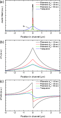
After solving Eq.3 for the fluctuation profile , we take its derivative with respect to and obtain the second factor of the integrand in Eq.1. Figs.9a-c compare the absorption heat source, the resulting profile, and its derivative for a representative GPD in presence of a plasmonic split-gate at different heights over the SLG channel, to an unperturbed fundamental dielectric waveguide mode, where the p-n junction is generated by a transparent (at the chosen ) gate, such as a split-gate made from a second SLG at a separation large enough to avoid additional optical losses. The beneficial role of plasmonic enhancement, with all other parameters fixed, for a sharper increase in translates to larger if the SLG channel is kept close to the SPP waveguide (50nm).
To model along the channel, we assume that the structure is gated to achieve the maximum below the gates, as for Eq.2 (opposite in sign but equal in magnitude for the p-n case) and approximate the gap region with a linear interpolation between the two. Combining both factors in Eq.1 and computing the integral yields or (if divided by ) as figure of merit to assess different cross section designs:
| (6) |
To calculate or photovoltage maps as in Fig.6b, we first generate the profile for all voltage combinations and then proceed via Eqs.6 or 1.
We then perform a sweep of gap width, SLG position, gate oxide thickness, gate contact height as a function of in SLG and . As for Fig.9, shorter distances between SLG channel and SPP waveguide yield larger signals. Furthermore, the SPP waveguide width affects the expected photovoltage in two ways. 1) narrower confinement improves the field strength at the SLG channel and at the cost of higher propagation losses; 2) the ungated SLG at the center of the device with not maximum shrinks with smaller gaps. The device parameters are then chosen based on these trends, taking into account fabrication complexity, robustness to processing-induced deviations (e.g. suppression of fundamental gap plasmon mode below a certain gap width), reliability (e.g. oxide break-down) and outcomes of FDTD simulations on coupling and propagation.
Extracting and of the fundamental mode in the hybrid region is sufficient for the design of the device cross-section. However, it does not capture the field distribution along the device, since optical losses, transition from dielectric to plasmonic waveguide, and power exchange between different modes that co-exist in the hybrid region remain unaccounted for. To find a good combination of SLG position and width within the constraints of the cross-section design, targeting a distribution with maximal derivative across the PD, but minimal along the propagation direction over the device length, we perform FDTD of the transition between SiN waveguide and GPD. We construct a device model in the same way as for the eigenmode analysis and adjust the source settings to 1.5-1.6m. We launch the fundamental quasi-TE mode of the SiN waveguide towards the GPD and use frequency domain field monitors (FDFM) with various orientations (parallel and perpendicular to the propagation direction) to track the field and power profiles at different points. Figs.10a-c plot the field at 3 cross-sections of a representative GPD. We see transitions from injected mode in dielectric waveguide to field distribution resembling the fundamental gap plasmon.
Figs.10d,e display the electric field intensity from a vertical FDMD monitor along the center line of the GPD, at two wavelengths. As expected for this non-adiabatic transition with fast decrease (1m) of the taper cross-section down to the target gap size, scattering and reflections at the start of the hybrid region reduce the power at the GPD, but the desired sharp intensity profile over length scales that match the fabricated SLG channel widths is achieved. Consequently, we place the SLG channel 100nm after the SPP structure has reached its final gap width. The comparison of field intensities for 1.5 and 1.6m on the same color scale in Figs.10d,e reveals a larger peak intensity and a longer interaction length for the latter, which indicates improved coupling efficiency at larger , as for the wavelength-depended in Fig.6c.
References
References
- (1) https://www.cisco.com/c/en/us/solutions/collateral/service-provider/visual-networking-index-vni/complete-white-paper-c11-481360.pdf
- (2) J. G. Andrews, S. Buzzi, W. Choi, S. V. Hanly, A. Lozano, A. C. K. Soong, and J. C. Zhang, IEEE J. Sel. Areas Commun. 32, 1065 (2014).
- (3) A. Osseiran, F. Boccardi, V. Braun, K. Kusume, P. Marsch, M. Maternia, O. Queseth, M. Schellmann, H. Schotten, H. Taoka et al., IEEE Commun. Mag. 52, 26 (2014).
- (4) https://community.arm.com/cfs-file/key/telligent-evolution-components-attachments/01-1996-00-00-00-01-30-09/Arm-2D00-The-route-to-a-trillion-devices-2D00-June-2017.pdf
- (5) S. Rumley, D. Nikolova, R. Hendry, Q. Li, D. Calhoun, and K. Bergman, J. Light. Technol. 33, 547 (2015).
- (6) Z. Zhou, R. Chen, X. Li, and T. Li, Opt. Fiber Technol. 44, 13 (2018).
- (7) G. T. Reed, Silicon Photonics: The State of the Art (John Wiley & Sons, Chichester, 2008).
- (8) D. Thomson, A. Zilkie, J. E. Bowers, T. Komljenovic, G. T. Reed, L. Vivien, D. Marris-Morini, E. Cassan, L. Virot, J. Fédéli et al., J. Opt. 18, 073003 (2016).
- (9) P. P. Absil, P. Verheyen, P. De Heyn, M. Pantouvaki, G. Lepage, J. De Coster, and J. Van Campenhout, Opt. Express 23, 9369 (2015).
- (10) A. H. Atabaki, S. Moazeni, F. Pavanello, H. Gevorgyan, J. Notaros, L. Alloatti, M. T. Wade, C. Sun, S. A. Kruger, H. Meng et al., Nature 556, 349 (2018).
- (11) A. Biberman, and K. Bergman, Rep. Prog. Phys. 75, 046402 (2012).
- (12) E. L. Wooten, K. M. Kissa, A. Yi-Yan, E. J. Murphy, D. A. Lafaw, P. F. Hallemeier, D. Maack, D. V. Attanasio, D. J. Fritz, G. J. McBrien et al., IEEE J. Sel. Topics Quantum Electron. 6, 69 (2000).
- (13) R. Nagarajan, M. Kato, J. Pleumeekers, P. Evans, S. Corzine, S. Hurtt, A. Dentai, S. Murthy, M. Missey, R. Muthiah et al., IEEE J. Sel. Topics Quantum Electron. 16, 1113 (2010).
- (14) G. T. Reed, G. Mashanovich, F. Y. Gardes, and D. J. Thomson, Nat. Photonics 4, 518 (2010).
- (15) G. T. Reed, G. Z. Mashanovich, F. Y. Gardes, M. Nedeljkovic, Y. Hu, D. J. Thomson, K. Li, P. R. Wilson, S. Chen, and S. S. Hsu, Nanophotonics 3, 229 (2014).
- (16) B. Seraphin, and N. Bottka, Phys. Rev. 139, A560 (1965).
- (17) J. Liu, M. Beals, A. Pomerene, S. Bernardis, R. Sun, J. Cheng, L. C. Kimerling, and J. Michel, Nat. Photonics 2, 433 (2008).
- (18) S. A. Srinivasan, M. Pantouvaki, S. Gupta, H. T. Chen, P. Verheyen, G. Lepage, G. Roelkens, K. Saraswat, D. Van Thourhout, P. Absil et al., J. Light. Technol. 34, 419 (2016).
- (19) J. Michel, J. Liu, and L. C. Kimerling, Nat. Photonics 4, 527 (2010).
- (20) A. R. Hawkins, W. Wu, P. Abraham, K. Streubel, and J. E. Bowers, Appl. Phys. Lett. 70, 303 (1997).
- (21) H. Chang, Y. Kuo, R. Jones, A. Barkai, and J. E. Bowers, Opt. Express 18, 23891 (2010).
- (22) L. Chrostowski, and M. Hochberg, Silicon Photonics Design: From Devices to Systems (Cambridge University Press, Glasgow, 2015).
- (23) L. Vivien, J. Osmond, J. Fédéli, D. Marris-Morini, P. Crozat, J. Damlencourt, E. Cassan, Y. Lecunff, and S. Laval, Opt. Express 17, 6252 (2009).
- (24) C. T. DeRose, D. C. Trotter, W. A. Zortman, A. L. Starbuck, M. Fisher, M. R. Watts, and P. S. Davids, Opt. Express 19, 24897 (2011).
- (25) L. Vivien, A. Polzer, D. Marris-Morini, J. Osmond, J. M. Hartmann, P. Crozat, E. Cassan, C. Kopp, H. Zimmermann, and J. M. Fédéli, Opt. Express 20, 1096 (2012).
- (26) A. Novack, M. Gould, Y. Yang, Z. Xuan, M. Streshinsky, Y. Liu, G. Capellini, A. E. Lim, G. Lo, T. Baehr-Jones et al., Opt. Express 21, 28387 (2013).
- (27) H. Chen, P. Verheyen, P. De Heyn, G. Lepage, J. De Coster, S. Balakrishnan, W. Yao, L. Shen, G. Roelkens, and J. Van Campenhout, Opt. Express 24, 4622 (2016).
- (28) J. Wang, and S. Lee, Sensors 11, 696 (2011).
- (29) H. Ye, and J. Yu, Sci. Technol. Adv. Mater. 15, 024601 (2014).
- (30) V. Sorianello, A. De Iacovo, L. Colace, A. Fabbri, L. Tortora, E. Buffagni, and G. Assanto, Appl. Phys. Lett. 101, 081101 (2012).
- (31) J. Liu, D. D. Cannon, K. Wada, Y. Ishikawa, S. Jongthammanurak, D. T. Danielson, J. Michel, and L. C. Kimerling, Appl. Phys. Lett. 87, 011110 (2005).
- (32) M. Romagnoli, V. Sorianello, M. Midrio, F. H. L. Koppens, C. Huyghebaert, D. Neumaier, P. Galli, W. Templ, A. D’Errico, and A. C. Ferrari, Nat. Rev. Mater. 3, 392–414 (2018).
- (33) M. Liu, X. Yin, E. Ulin-Avila, B. Geng, T. Zentgraf, L. Ju, F. Wang, and X. Zhang, Nature 474, 64 (2011).
- (34) M. Liu, X. Yin, and X. Zhang, Nano Lett. 12, 1482 (2012).
- (35) Y. Hu, M. Pantouvaki, J. Van Campenhout, S. Brems, I. Asselberghs, C. Huyghebaert, P. Absil, and D. Van Thourhout, Laser Photon. Rev. 10, 307 (2016).
- (36) C. T. Phare, Y. Daniel Lee, J. Cardenas, and M. Lipson, Nat. Photonics 9, 511 (2015).
- (37) V. Sorianello, M. Midrio, and M. Romagnoli, Opt. Express 23, 6478 (2015).
- (38) V. Sorianello, M. Midrio, G. Contestabile, I. Asselberghs, J. Van Campenhout, C. Huyghebaert, I. Goykhman, A. K. Ott, A. C. Ferrari, and M. Romagnoli, Nat. Photonics 12, 40 (2018).
- (39) Z. Sun, A. Martinez, and F. Wang, Nat. Photonics 10, 227 (2016).
- (40) X. Gan, R. Shiue, Y. Gao, I. Meric, T. F. Heinz, K. Shepard, J. Hone, S. Assefa, and D. Englund, Nat. Photonics 7, 883 (2013).
- (41) A. Pospischil, M. Humer, M. M. Furchi, D. Bachmann, R. Guider, T. Fromherz, and T. Mueller, Nat. Photonics 7, 892 (2013).
- (42) X. Wang, Z. Cheng, K. Xu, H. K. Tsang, and J. Xu, Nat. Photonics 7, 888 (2013).
- (43) I. Goykhman, U. Sassi, B. Desiatov, N. Mazurski, S. Milana, D. De Fazio, A. Eiden, J. Khurgin, J. Shappir, U. Levy et al., Nano Lett. 16, 3005 (2016).
- (44) D. Schall, D. Neumaier, M. Mohsin, B. Chmielak, J. Bolten, C. Porschatis, A. Prinzen, C. Matheisen, W. Kuebart, B. Junginger et al., ACS Photonics 1, 781 (2014).
- (45) S. Schuler, D. Schall, D. Neumaier, L. Dobusch, O. Bethge, B. Schwarz, M. Krall, and T. Mueller, Nano Lett. 16, 7107 (2016).
- (46) S. Schuler, D. Schall, D. Neumaier, B. Schwarz, K. Watanabe, T. Taniguchi, and T. Mueller, ACS Photonics 5, 4758 (2018).
- (47) R. J. Shiue, Y. Gao, Y. Wang, C. Peng, A. D. Robertson, D. K. Efetov, S. Assefa, F. H. L. Koppens, J. Hone, and D. Englund, Nano Lett. 15, 7288 (2015).
- (48) D. Schall, C. Porschatis, M. Otto, and D. Neumaier, J. Phys. D: Appl. Phys. 50, 124004 (2017).
- (49) D. Schall, E. Pallecchi, G. Ducournau, V. Avramovic, M. Otto, and D. Neumaier, in Optical Fiber Communication Conference, M2I.4, (Optical Society of America, 2018).
- (50) Y. Ding, Z. Cheng, X. Zhu, K. Yvind, J. Dong, M. Galili, H. Hu, N. A. Mortensen, S. Xiao, and L. K. Oxenløwe, arXiv: 1808.04815 (2018).
- (51) P. Ma, Y. Salamin, B. Baeuerle, A. Josten, W. Heni, A. Emboras, and J. Leuthold, ACS Photonics 6, 154 (2019).
- (52) Z. Ma, K. Kikunage, H. Wang, S. Sun, R. Amin, M. Tahersima, R. Maiti, M. Miscuglio, H. Dalir, and V. J. Sorger, arXiv: 1812.00894 (2018).
- (53) F. Bonaccorso, Z. Sun, T. Hasan, and A. C. Ferrari, Nat. Photonics 4, 611 (2010).
- (54) A. Urich, K. Unterrainer, and T. Mueller, Nano Lett. 11, 2804 (2011).
- (55) F. Xia, T. Mueller, Y. Lin, A. Valdes-Garcia, and P. Avouris, Nat. Nanotechnol. 4, 839 (2009).
- (56) R. R. Nair, P. Blake, A. N. Grigorenko, K. S. Novoselov, T. J. Booth, T. Stauber, N. M. R. Peres, and A. K. Geim, Science 320, 1308 (2008).
- (57) J. M. Dawlaty, S. Shivaraman, J. Strait, P. George, M. Chandrashekhar, F. Rana, M. G. Spencer, D. Veksler, and Y. Chen, Appl. Phys. Lett. 93, 131905 (2008).
- (58) F. H. Koppens, T. Mueller, P. Avouris, A. C. Ferrari, M. S. Vitiello, and M. Polini, Nat. Nanotechnol. 9, 780 (2014).
- (59) S. Goossens, G. Navickaite, C. Monasterio, S. Gupta, J. J. Piqueras, R. Pérez, G. Burwell, I. Nikitskiy, T. Lasanta, T. Galán et al., Nat. Photonics 11, 366 (2017).
- (60) N. Youngblood, and M. Li, Nanophotonics 6, 1205 (2017).
- (61) M. Liu, and X. Zhang, Nat. Photonics 7, 851 (2013).
- (62) K. Tielrooij, L. Piatkowski, M. Massicotte, A. Woessner, Q. Ma, Y. Lee, K. S. Myhro, C. N. Lau, P. Jarillo-Herrero, N. F. van Hulst et al., Nat. Nanotechnol. 10, 437 (2015).
- (63) T. Mueller, F. Xia, and P. Avouris, Nat. Photonics 4, 297 (2010).
- (64) T. J. Echtermeyer, P. S. Nene, M. Trushin, R. V. Gorbachev, A. L. Eiden, S. Milana, Z. Sun, J. Schliemann, E. Lidorikis, K. S. Novoselov et al., Nano Lett. 14, 3733 (2014).
- (65) J. C. W. Song, M. S. Rudner, C. M. Marcus, and L. S. Levitov, Nano Lett. 11, 4688 (2011).
- (66) N. M. Gabor, J. C. Song, Q. Ma, N. L. Nair, T. Taychatanapat, K. Watanabe, T. Taniguchi, L. S. Levitov, and P. Jarillo-Herrero, Science 334, 648 (2011).
- (67) G. Konstantatos, M. Badioli, L. Gaudreau, J. Osmond, M. Bernechea, F. P. G. de Arquer, F. Gatti, and F. H. L. Koppens, Nat. Nanotechnol. 7, 363 (2012).
- (68) L. Vicarelli, M. S. Vitiello, D. Coquillat, A. Lombardo, A. C. Ferrari, W. Knap, M. Polini, V. Pellegrini, and A. Tredicucci, Nat. Mater. 11, 865 (2012).
- (69) M. Freitag, T. Low, F. Xia, and P. Avouris, Nat. Photonics 7, 53 (2013).
- (70) U. Sassi, R. Parret, S. Nanot, M. Bruna, S. Borini, D. De Fazio, Z. Zhao, E. Lidorikis, F. H. L. Koppens, A. C. Ferrari et al., Nat. Commun. 8, 14311 (2017).
- (71) N. Huo, and G. Konstantatos, Adv. Mater. 30, 1801164 (2018).
- (72) D. Brida, A. Tomadin, C. Manzoni, Y. J. Kim, A. Lombardo, S. Milana, R. R. Nair, K. S. Novoselov, A. C. Ferrari, G. Cerullo et al., Nat. Commun. 4, 1987 (2013).
- (73) A. Tomadin, D. Brida, G. Cerullo, A. C. Ferrari, and M. Polini, Phys. Rev. B 88, 035430 (2013).
- (74) C. Kittel, Introduction to solid state physics (Wiley New York, New York, 1996).
- (75) N. Bonini, M. Lazzeri, N. Marzari, and F. Mauri, Phys. Rev. Lett. 99, 176802 (2007).
- (76) M. Lazzeri, S. Piscanec, F. Mauri, A. Ferrari, and J. Robertson, Phys. Rev. Lett. 95, 236802 (2005).
- (77) N. Ashcroft, and N. Mermin, Solid State Physics (Harcourt College Publishers, Fort Worth, 1976).
- (78) Q. Ma, N. M. Gabor, T. I. Andersen, N. L. Nair, K. Watanabe, T. Taniguchi, and P. Jarillo-Herrero, Phys. Rev. Lett. 112, 247401 (2014).
- (79) M. Freitag, T. Low, and P. Avouris, Nano Lett. 13, 1644 (2013).
- (80) P. K. Herring, A. L. Hsu, N. M. Gabor, Y. C. Shin, J. Kong, T. Palacios, and P. Jarillo-Herrero, Nano Lett. 14, 901 (2014).
- (81) S. Castilla, B. Terres, M. Autore, L. Viti, J. Li, A. Nikitin, I. Vangelidis, K. Watanabe, T. Taniguchi, E. Lidorikis et al., Nano Lett. , (2019).
- (82) K. S. Novoselov, D. Jiang, F. Schedin, T. J. Booth, V. V. Khotkevich, S. V. Morozov, and A. K. Geim, Proc. Natl. Acad. Sci. U.S.A. 102, 10451 (2005).
- (83) L. Wang, I. Meric, P. Y. Huang, Q. Gao, Y. Gao, H. Tran, T. Taniguchi, K. Watanabe, L. M. Campos, D. A. Muller et al., Science 342, 614 (2013).
- (84) D. G. Purdie, N. M. Pugno, T. Taniguchi, K. Watanabe, A. C. Ferrari, and A. Lombardo, Nat. Commun. 9, 5387 (2018).
- (85) D. De Fazio, D. G. Purdie, A. K. Ott, P. Braeuninger-Weimer, T. Khodkov, S. Goossens, T. Taniguchi, K. Watanabe, P. Livreri, F. H. L. Koppens et al., arXiv: 1904.01405 (2019).
- (86) V. Miseikis, F. Bianco, J. David, M. Gemmi, V. Pellegrini, M. Romagnoli, and C. Coletti, 2D Mater. 4, 021004 (2017).
- (87) X. Li, C. W. Magnuson, A. Venugopal, J. An, J. W. Suk, B. Han, M. Borysiak, W. Cai, A. Velamakanni, Y. Zhu et al., Nano Lett. 10, 4328 (2010).
- (88) B. Wang, M. Huang, L. Tao, S. H. Lee, A. Jang, B. Li, H. S. Shin, D. Akinwande, and R. S. Ruoff, ACS Nano 10, 1404 (2016).
- (89) J. W. Suk, A. Kitt, C. W. Magnuson, Y. Hao, S. Ahmed, J. An, A. K. Swan, B. B. Goldberg, and R. S. Ruoff, ACS Nano 5, 6916 (2011).
- (90) I. Goykhman, B. Desiatov, J. Khurgin, J. Shappir, and U. Levy, Nano Lett. 11, 2219 (2011).
- (91) I. Goykhman, B. Desiatov, J. Khurgin, J. Shappir, and U. Levy, Opt. Express 20, 28594 (2012).
- (92) Y. Salamin, P. Ma, B. Baeuerle, A. Emboras, Y. Fedoryshyn, W. Heni, B. Cheng, A. Josten, and J. Leuthold, ACS Photonics 5, 3291 (2018).
- (93) T. J. Echtermeyer, L. Britnell, P. K. Jasnos, A. Lombardo, R. V. Gorbachev, A. N. Grigorenko, A. K. Geim, A. C. Ferrari, and K. S. Novoselov, Nat. Commun. 2, 455 (2011).
- (94) Z. Fang, Z. Liu, Y. Wang, P. M. Ajayan, P. Nordlander, and N. J. Halas, Nano Lett. 12, 3808 (2012).
- (95) T. J. Echtermeyer, S. Milana, U. Sassi, A. Eiden, M. Wu, E. Lidorikis, and A. C. Ferrari, Nano Lett. 16, 8 (2016).
- (96) C. Chen, N. Youngblood, R. Peng, D. Yoo, D. A. Mohr, T. W. Johnson, S. Oh, and M. Li, Nano Lett. 17, 985 (2017).
- (97) B. Desiatov, I. Goykhman, and U. Levy, Nano Lett. 14, 648 (2014).
- (98) W. Shin, A. Raman, and S. Fan, J. Opt. Soc. Am. B 29, 1048 (2012).
- (99) J. Tian, S. Yu, W. Yan, and M. Qiu, Appl. Phys. Lett. 95, 013504 (2009).
- (100) G. Dabos, D. Ketzaki, A. Manolis, E. Chatzianagnostou, L. Markey, J. Weeber, A. Dereux, A. L. Giesecke, C. Porschatis, B. Chmielak et al., IEEE Photon. J. 10, 2700308 (2018).
- (101) Q. Li, and M. Qiu, Opt. Express 18, 15531 (2010).
- (102) C. Delacour, S. Blaize, P. Grosse, J. M. Fedeli, A. Bruyant, R. Salas-Montiel, G. Lerondel, and A. Chelnokov, Nano Lett. 10, 2922 (2010).
- (103) A. Lagatsky, Z. Sun, T. Kulmala, R. Sundaram, S. Milana, F. Torrisi, O. Antipov, Y. Lee, J. Ahn, C. Brown et al., Appl. Phys. Lett. 102, 013113 (2013).
- (104) A. C. Ferrari, J. C. Meyer, V. Scardaci, C. Casiraghi, M. Lazzeri, F. Mauri, S. Piscanec, D. Jiang, K. S. Novoselov, S. Roth et al., Phys. Rev. Lett. 97, 187401 (2006).
- (105) A. C. Ferrari, and D. M. Basko, Nat. Nanotechnol. 8, 235 (2013).
- (106) A. Das, S. Pisana, B. Chakraborty, S. Piscanec, S. K. Saha, U. V. Waghmare, K. S. Novoselov, H. R. Krishnamurthy, A. K. Geim, A. C. Ferrari et al., Nat. Nanotechnol. 3, 210 (2008).
- (107) D. M. Basko, S. Piscanec, and A. C. Ferrari, Phys. Rev. B 80, 165413 (2009).
- (108) K. S. Novoselov, A. K. Geim, S. V. Morozov, D. Jiang, Y. Zhang, S. V. Dubonos, I. V. Grigorieva, and A. A. Firsov, Science 306, 666 (2004).
- (109) J. M. Senior, and M. Y. Jamro, Optical fiber communications: principles and practice (Pearson Education, Harlow, 2009).
- (110) J. Diels, and W. Rudolph, Ultrashort laser pulse phenomena (Elsevier, London, 2006).
- (111) N. K. Emani, A. V. Kildishev, V. M. Shalaev, and A. Boltasseva, Nanophotonics 4, 214 (2015).
- (112) G. W. Hanson, J. Appl. Phys. 103, 064302 (2008); ibid. 113, 029902 (2013).
- (113) G. T. Reed, and A. P. Knights, Silicon Photonics: An Introduction (John Wiley & Sons, Chichester, 2004).
- (114) G. Soavi, G. Wang, H. Rostami, D. G. Purdie, D. De Fazio, T. Ma, B. Luo, J. Wang, A. K. Ott, D. Yoon et al., Nat. Nanotechnol. 13, 583 (2018).
- (115) G. Soavi, G. Wang, H. Rostami, A. Tomadin, O. Balci, I. Paradeisanos, E. Pogna, G. Cerullo, E. Lidorikis, M. Polini et al., arXiv: 1903.00989 (2019).