Determining the depairing current in superconducting
nanowire single-photon detectors
Abstract
We estimate the depairing current of superconducting nanowire single-photon detectors (SNSPDs) by studying the dependence of the nanowires’ kinetic inductance on their bias current. The kinetic inductance is determined by measuring the resonance frequency of resonator-style nanowire coplanar waveguides both in transmission and reflection configurations. Bias current dependent shifts in the measured resonant frequency correspond to the change in the kinetic inductance, which can be compared with theoretical predictions. We demonstrate that the fast relaxation model described in the literature accurately matches our experimental data and provides a valuable tool for direct determination of the depairing current. Accurate and direct measurement of the depairing current is critical for nanowire quality analysis, as well as modeling efforts aimed at understanding the detection mechanism in SNSPDs.
I Introduction
Superconducting nanowire single-photon detectors (SNSPDs) Gol’tsman et al. 2001 are established as a key technology for many applications, such as deep-space optical communication, laser ranging and quantum science. This is due to their high efficiency ( 90%) Marsili et al. 2013, wide wavelength sensitivity (from X-rays to mid-infrared) Zhang, Wang, and Schilling 2016; Korneev et al. 2012, low dark count rate ( 1 Hz) Wollman et al. 2017 and ultra-high timing resolution ( 3 ps) Korzh et al..
In the last decade, widespread effort by the SNSPD community has improved the theoretical understanding of the detection mechanism in SNSPDs. Guided by experimental measurements Kerman et al. 2007; Engel et al. 2013; Renema et al. 2014; Lusche et al. 2014; Renema et al. 2015; Marsili et al. 2016; Gaudio et al. 2016; Caloz et al. 2017 and theoretical modeling Bulaevskii, Graf, and Kogan 2012; Vodolazov et al. 2015; Kozorezov et al. 2015; Engel et al. 2015; Vodolazov 2017; Kozorezov et al. 2017, it is currently understood that most features of photodetection in SNSPDs can be explained by a combination of Fano fluctuations Kozorezov et al. 2017 and vortex-based breaking of superconductivity Vodolazov et al. 2015. More recently, the measurement of record low timing jitter Korzh et al. has led to a new effort in understanding the latency of SNSPDs Allmaras et al. in order to predict the intrinsic timing jitter of these detectors. It is known that a precise estimate of the depairing current of a device is needed in order to match experimental results using these models. The most common way of estimating the depairing current is through the Kupryianov-Lukichev formula Kupriyanov and Lukichev 1980, which requires several independent material parameters such as the diffusion coefficient, sheet resistance, critical temperature and nanowire geometry. In this work, we demonstrate a direct method of accessing the depairing current by measuring the kinetic inductance change as a function of the bias current. This method relies on fitting the theoretical dependence calculated by Clem and Kogan Clem and Kogan 2012 where the depairing current is the single free fitting parameter. Having access to a direct measurement of the depairing current enables a better estimation of the figure of merit for the quality of superconducting nanowires: the constriction factor Kerman et al. 2007, ratio of the switching and depairing currents (), since reaching higher fractions of the depairing current gives rise to higher internal detection efficiency and lower intrinsic jitter Korzh et al..
The kinetic inductance dependence on bias current is determined by measuring the self-resonance of a superconducting nanowire in a coplanar waveguide (CPW) structure, using a vector network analyzer (VNA). The resonances were measured in both transmission and reflection modes by analyzing the complex spectral response. Measurement of the self-resonance has been demonstrated for meandered nanowires Santavicca et al. 2016, however, the change of the kinetic inductance at the highest achievable bias current relative to the zero bias current case was less than 10%, making it difficult to distinguish whether the experiment falls within the fast or slow relaxation category and giving rise to significantly different depairing current predictions Clem and Kogan 2012. Here we demonstrate a kinetic-inductance change as high as 31% for tungsten silicide (WSi) and 28% for niobium nitride (NbN) nanowires, which allows us to conclude that the experiment falls into the fast relaxation regime by comparing the quality of the fit of the two models. The improvement could be attributed to several factors such as optimized material Dane et al. 2017, lower base temperature and use of a cryogenic bias-tee and amplifier.
We present the dependence of the measured depairing current on the width of the nanowire resonators as well as the operating temperature. An important observation is that reduces for higher operating temperatures for both polycrystalline NbN and amorphous WSi devices, which has significant consequences for design of high-performance SNSPDs at elevated temperatures. There is also an indication that narrower nanowires achieve a lower , which may point to nanowire edge roughness due to fabrication imperfections.
II Device Design and Fabrication

The nanowire resonators are designed in a CPW Zhao et al. 2017; Zhu et al. 2019 to avoid electromagnetic coupling within the meander and to allow for simplified impedance engineering. The resonance is set up by means of the impedance mismatch between the transmission line and the narrow nanowire. This approach simplifies current biasing of the nanowire. The devices were designed in order to have the resonant frequency at roughly 2 GHz, so that the microwave period ( 500 ps) is much larger than the relaxation time of the superconducting order parameter for both WSi Zhang et al. 2018a and NbN Zhang et al. 2018b. An estimate of the relaxation time of the order parameter is given by , so for NbN films ( 8.65 K) the order parameter relaxation time is 1 ps, while for WSi films ( 3.50 K) it is 3.1 ps, at a temperature of 1.05 K. At the highest temperature investigated ( for NbN and for WSi) the order parameter relaxation time is 4.6 ps and 7.3 ps, for NbN and WSi films, respectively.
The devices were fabricated from a 6 nm thick NbN film and from a 7 nm thick WSi film. NbN film was sputter deposited on a 4-inch silicon wafer with a 300 nm thick thermal oxide layer Dane et al. 2017. WSi was sputter deposited on 4-inch silicon wafer with a 240 nm thick thermal oxide layer and was passivated with a 15 nm thick silicon dioxide (SiO2) film. All the devices and pad structures were patterned using electron beam lithography with gL2000 positive tone resist Zhao et al. 2017. The patterns were then transferred into NbN and WSi by CF4 reactive ion etching. A layer of HSQ was spun on the dies after fabrication, for passivation.
III Experimental Setup
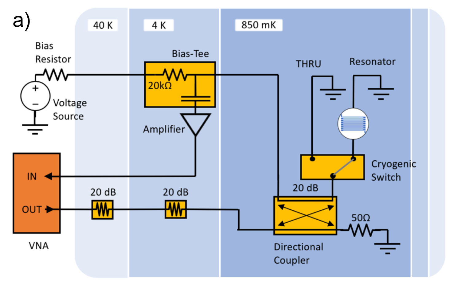
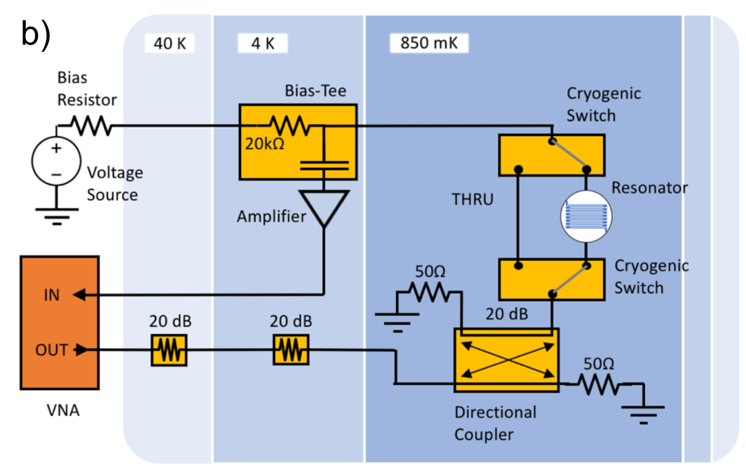
The experimental setup is illustrated in Fig. 2. We measured the resonant frequency of the SNSPD-like resonators (Fig. 1) both in transmission mode Santavicca et al. 2016 and in reflection mode (Fig. 2). The devices were cooled to a base temperature of 1.05 K with a cryocooler composed of a pulse tube followed by a Helium-4 sorption cooler.
The device resonance was measured with a 300 kHz-6 GHz VNA. The output signal from the VNA was attenuated by 20 dB at both the 40 K and 4 K stages, before entering the input port of a 20 dB directional coupler. The transmission port of the coupler was 50 terminated, while the coupling port, was connected to an RF switch on the 1 K stage. One port of the switch was connected to a through device, which consisted of a superconducting CPW used for calibration purposes. The RF switch was used to achieve the same electrical environment between the calibration device and the device under test.
While measuring in the transmission mode, the output port of the resonator CPW, was connected to a second switch followed by a cryogenic bias tee. The DC port was used to current bias the nanowire, while the RF port was fed to the input of a SiGe cryogenic amplifier (Cosmic Microwave, CITLF1 11 1 The use of trade names is intended to allow the measurements to be appropriately interpreted and does not imply endorsement by the US government, nor does it imply these are necessarily the best available for the purpose used here.). The bias tee and amplifier were mounted and thermalized to the 4 K stage. The amplified RF signal was fed to the input port of the VNA. Finally, the isolated port of the directional coupler was 50 terminated to guarantee current flow through the nanowire. In reflection mode, the nanowire was connected to the coupler on one side and grounded on the other. In this configuration, the isolation port of the directional coupler connected the nanowire to the bias tee and amplifier. For both scenarios, the power output of the VNA was adjusted such that the RMS current flowing through the resonator was of the order of 100 nA, which is small to prevent a shift in the resonant frequency.


IV Models
The measured resonance peaks were fitted using a RLC resonator model with a purely reactive bypass channel. For the reflection mode measurement, the resonance was fitted using a double notch filter at the resonant frequency. The magnitude and phase functions of are written as
| (1a) | ||||
| (1b) | ||||
where is the full-width at half-maximum of the Lorentzian function, is the peak height, is the resonant frequency and is the quality factor.
For the transmission mode measurement, the resonance is still been modeled as a Lorentzian function, but accounts for the effect of a bypass channel, modeled as a pure capacitance, in a correction factor. We define according to
| (2) |
where the correction factor to the Lorentzian function in (2) is valid for purely reactive bypass channels and is a constant representing the coupling between the resonator and the reactive channel. For further information regarding the physical meaning of , we direct readers to the supplementary information of Weinstein and Schwab Weinstein et al. 2014.
Once the resonant frequency of the nanowire was evaluated, we could estimate the change in kinetic inductance with increasing bias current according to for an RLC resonator. We then fitted the kinetic inductance ratios as obtained using the two relaxation models from Clem and Kogan Clem and Kogan 2012
| (3a) | ||||
| (3b) | ||||
where is the ratio between the kinetic inductance of the biased superconducting nanowire and the kinetic inductance at zero bias current, and are fixed parameters defined by Clem and Kogan Clem and Kogan 2012 for specific temperature ratios , is the ratio between the bias current density and the depairing current density and the subscripts “fr” and “sr” stand for “fast relaxation” and “slow relaxation” respectively. The difference between the two models is related to the characteristic timescale of variation of , the current-biased experiment characteristic time , with respect to the relaxation time of the superconductor (). We refer to fast relaxation if the experimental time constant is much larger than the characteristic superconductor relaxation time, while for slow relaxation, the experimental time constant is much smaller. The accuracy of the fitting functions (3a) and (3b) compared to the full numerical solution presented in Clem and Kogan 2012 is 1% for the fast relaxation model and 0.5% for the slow relaxation model. As a comparison, we also calculate the depairing current using a fit to the full numerical results of the fast relaxation model using the approach of Clem and Kogan 2012 and keeping 15000 modes in the numerical calculations. The numerical results provide a better match to the experimental results than the approximate equation with only a small change in the extracted depairing current when compared to the approximate fit of (3a). Within both models, the depairing current density is the only fitting parameter.
V Results
We measured the resonant frequencies of nanowire devices with widths of typical SNSPDs (50-200 nm) using both NbN and WSi thin films.
The resonance features of an NbN, 120nm wide device, measured at zero current and close to the switching bias current () are shown in Fig. 3. The fit of the models described in section IV is shown in red for both the transmission (Fig. 3a, where we use (2) to fit the magnitude) and reflection (Fig. 3b, where we use (1b) to fit the phase) measurements. For the phase analysis, we found it best to normalize the phase data with respect to the phase of the resonator while in non-superconducting state, i.e. biasing the device above its switching current. The resonant peaks obtained using the two different methods of reflection and transmission match within 0.5%; however, from the goodness of the two fits, we decided to prioritize the analysis of the phase in reflection method as it is, in general, less noisy and requires fewer free parameters to perform the fit. From this point onward we only refer to data collected from the phase response of the resonator in reflection mode.


The kinetic inductance ratios, obtained by the measured resonance frequencies as,
| (4) |
are then plotted in Fig. 3c a function of the bias current. The fast relaxation and slow relaxation models discussed by Clem and Kogan Clem and Kogan 2012 have been fitted to the data, where the only free parameter is the depairing current of the nanowire. The estimated depairing current for each model can be found in the caption of Fig. 3.
It is immediately clear from Fig. 3c that the fast relaxation model provides a better fit of the experimental data than the slow relaxation model. Moreover, the depairing current evaluated using the latter model appears to be unreliable since the model predicts depairing currents just above the measured switching currents. Due to fabrication imperfections, the measured switching currents in SNSPDs are typically significantly below the depairing current since the switching current is set by the weakest point along the nanowire, typically referred to as a constriction. The depairing current, however, is an average characteristic of the nanowire, hence a switching current approaching the depairing current would suggest a ”perfect” nanowire. By removing the highest bias current points, it is possible to simulate a more constricted nanowire, while the measured depairing current should remain unchanged. Carrying out this exercise, the slow relaxation model does not predict constant values while the fast relaxation model is robust and provides depairing current estimates which are more consistent with theoretical models. With this, we conclude that our experiment falls into the fast relaxation regime, which has not been confirmed previously Santavicca et al. 2016.
We measured the resonant frequency of the nanowires with respect to biasing at different temperature conditions. This measurement was done to compare the temperature dependence of the depairing current with the theoretical predictions. The NbN nanowires resonance frequencies were collected starting from the base temperature 1.05 K up to 7.00 K, which is more than 80% of the superconductor transition temperature, measured to be 8.65 K, while the WSi devices were measured up to 2.45 K, which corresponds to 70% of their of 3.50 K. The constriction factor drops with increasing temperature for both NbN and WSi devices. This effect might be due to local defects in the nanowire structure: if the weakest constriction in the nanowire has a lower transition temperature then its local switching current would drop faster than the depairing current for the whole nanowire, with increasing operating temperature. This observation deserves future investigation, since it could shed light on the possibility of SNSPD operation at elevated temperatures.
In total, we tested one die with two NbN device geometries (widths of 120 and 140 nm) and two identical dies with five WSi device geometries each (widths of 55, 80, 120, 160 and 200 nm). The measured switching currents and the estimated critical depairing currents based on the fast and the slow relaxation models are collected in Table 1. In Fig. 4a we report the trend of the devices’ critical depairing currents with respect to different temperatures. We estimate the zero temperature depairing current by fitting the measured temperature dependence of to the function defining the temperature dependence of the numerical solution to the Usadel equations. These estimated values for are collected in Table 1. For comparison, we also calculated the theoretical critical depairing current at zero temperature according to Kupryianov and Lukichev model Kupriyanov and Lukichev 1980, denoted as:
| (5) |
where is the electron charge, is the single-spin electron density of states at Fermi level in the normal state, is the superconducting gap at zero temperature, is the diffusion coefficient, is the square resistance, and and are width and thickness of the nanowire, respectively. In order to calculate these values, we measured the diffusion coefficient for WSi, while for NbN, we used a value found in literature.
| Device | Fast Relax Approximation | Fast Relax Numerical | Slow Relax Approximation | Measured | Estimated | |||||||
|---|---|---|---|---|---|---|---|---|---|---|---|---|
| Material | Width | Fit | Fit | Fit | ||||||||
| WSi | 55 nm | 4.40 | 0.9942 | 4.67 | 0.9990 | 3.32 | 0.7413 | 2.25 | 0.54 | 1.107 | 5.31* | 6.47 |
| WSi | 55 nm | 4.29 | 0.9924 | 4.59 | 0.9984 | 3.09 | 0.7998 | 2.13 | 0.49 | 1.085 | 5.09 | 6.47 |
| WSi | 80 nm | 7.58 | 0.9808 | 8.30 | 0.9962 | 4.74 | 0.9636 | 3.25 | 0.43 | 1.055 | 9.72 | 10.68 |
| WSi | 80 nm | 9.22 | 0.9955 | 9.81 | 0.9995 | 6.05 | 0.9838 | 4.75 | 0.52 | 1.094 | 11.66 | 10.68 |
| WSi | 120 nm | 14.62 | 0.9930 | 15.60 | 0.9996 | 9.47 | 0.9801 | 7.25 | 0.50 | 1.090 | 18.72 | 17.41 |
| WSi | 120 nm | 14.82 | 0.9940 | 16.25 | 0.9961 | 9.55 | 0.9834 | 6.75 | 0.46 | 1.066 | 20.31 | 17.41 |
| WSi | 160 nm | 20.76 | 0.9980 | 21.71 | 0.9986 | 13.82 | 0.9856 | 12.25 | 0.59 | 1.152 | 26.07 | 23.46 |
| WSi | 160 nm | 21.16 | 0.9970 | 21.98 | 0.9984 | 14.44 | 0.9750 | 13.50 | 0.64 | 1.179 | 25.98 | 23.46 |
| WSi | 200 nm | 27.65 | 0.9954 | 28.06 | 0.9993 | 21.00 | 0.7813 | 20.50 | 0.74 | 1.313 | 33.26 | 30.28 |
| NbN | 120 nm | 38.19 | 0.9975 | 38.78 | 1.0000 | 27.05 | 0.9239 | 26.50 | 0.69 | 1.280 | 42.07 | 43.30 |
| NbN | 140 nm | 46.93 | 0.9970 | 47.67 | 0.9999 | 33.09 | 0.9295 | 32.50 | 0.69 | 1.280 | 51.47 | 50.52 |
In order to calculate these values, we measured the temperature dependence of the upper critical magnetic field () and extracted information on material properties of the WSi thin film. The electron diffusion coefficient was obtained from the slope of the vs curve. In the limit of a dirty superconductor, the electron diffusivity can be expressed as follows, based on Semenov et al. 2009,
| (6) |
where the diffusion coefficient has dimensions of , the upper critical magnetic field has dimensions of [T] and the temperature has dimensions of [K].
The external magnetic field was applied perpendicular to the surface of the film and was defined as the field at which the resistance of the film becomes half of the normal state value. The calculated value for the electron diffusion coefficient, based on equation (6), is 0.74 for the 7 nm thick WSi film. The Ginzburg-Landau coherence length, , at can be extracted from the following equation:
| (7) |
where is the magnetic-flux quantum and is the electron charge.
In the limit of a dirty superconductor, a linear extrapolation of the measured down to , overestimates the real upper critical field at zero temperature and consequently underestimates the superconducting coherence length. A more realistic value of is given by
| (8) |
Using this value of in equation (7) the calculated coherence length is 9.62 nm for the 7 nm thick WSi film. For the 6 nm thick NbN film, we considered a diffusion coefficient of as used by Zhao et al. Zhao et al. 2017 and estimated a coherence length at zero temperature of 5.01 nm.
We measured the constriction factor, , which is the ratio between the switching and depairing current, at different temperature conditions for all the devices tested. This ratio can be considered as the quality of the nanowire itself. Shown in Fig. 4b, the ratio of currents suggests a decrease of quality of the devices with increasing temperature.

For the WSi devices, since five geometries were studied, we were able to show the dependence of the depairing current on the device width. As Fig. 5 shows a linear fit to the depairing current estimated at different temperatures seems to suggest that the effective widths of the nanowires might be reduced from the measured widths (SEM after etching) by an offset of nm. That effect could be caused by the loss of superconductivity in the edges of the nanowire due to scattering of particles during etching, or due to oxidation of the nanowire caused by exposure to the environment. It is worth noting that the offset is close to two times the superconducting coherence length of the WSi devices, so it is possible that poisoning of the edges of the nanowire during the fabrication process might have suppressed the superconducting active area by roughly one coherence length on each side. More work is needed to conclusively determine the the cause of this observation.
VI Conclusion
We have demonstrated a reproducible experimental setup able to estimate the depairing current of superconducting nanowires. According to our experimental data obtained by measuring both NbN and WSi nanowire resonators, the fast relaxation model discussed in the literature gives a more robust and reliable estimate of the depairing current. This experimental method, when combined with other device performance metrics such as the internal efficiency, can be used to refine detection mechanism models and improve the current understanding of the device physics of SNSPDs.
A direct estimation of the depairing current is essential in experimental tests of the relation between the device’s minimum photon energy sensitivity and the width of the SNSPD, which is a crucial aspect to take into account when designing SNSPD for specific wavelengths.
Finally, we introduced a new way to measure the quality of the devices in terms of the constriction factor , and we showed that this factor decreases with increasing temperature. The reason for this decrease would make an interesting topic for future study.
Acknowledgements
Part of this research was performed at the Jet Propulsion Laboratory, California Institute of Technology, under contract with the National Aeronautics and Space Administration. Support for this work was provided in part by the DARPA Defense Sciences Office, through the DETECT program. J. P. A. acknowledges partial support from the NASA Space Technology Research Fellowship program. D. Z. acknowledges support from the A*STAR National Science Scholarship.
References
- Gol’tsman et al. (2001) G. N. Gol’tsman, O. Okunev, G. Chulkova, A. Lipatov, A. Semenov, K. Smirnov, B. Voronov, A. Dzardanov, C. Williams, and R. Sobolewski, Appl. Phys. Lett. 79, 705 (2001).
- Marsili et al. (2013) F. Marsili, V. B. Verma, J. A. Stern, S. Harrington, A. E. Lita, T. Gerrits, I. Vayshenker, B. Baek, M. D. Shaw, R. P. Mirin, and S. W. Nam, Nature Photonics 7, 210 EP (2013).
- Zhang, Wang, and Schilling (2016) X. Zhang, Q. Wang, and A. Schilling, AIP Advances 6, 115104 (2016), https://doi.org/10.1063/1.4967278 .
- Korneev et al. (2012) A. Korneev, Y. Korneeva, I. Florya, B. Voronov, and G. Goltsman, Physics Procedia 36, 72 (2012), sUPERCONDUCTIVITY CENTENNIAL Conference 2011.
- Wollman et al. (2017) E. E. Wollman, V. B. Verma, A. D. Beyer, R. M. Briggs, B. Korzh, J. P. Allmaras, F. Marsili, A. E. Lita, R. P. Mirin, S. W. Nam, and M. D. Shaw, Opt. Express 25, 26792 (2017).
- (6) B. A. Korzh, Q.-Y. Zhao, S. Frasca, J. P. Allmaras, T. M. Autry, E. A. Bersin, M. Colangelo, G. M. Crouch, A. E. Dane, T. Gerrits, F. Marsili, G. Moody, E. Ramirez, J. D. Rezac, M. J. Stevens, E. E. Wollman, D. Zhu, P. D. Hale, K. L. Silverman, R. P. Mirin, S. W. Nam, M. D. Shaw, and K. K. Berggren, arXiv:1804.06839 .
- Kerman et al. (2007) A. J. Kerman, E. A. Dauler, J. K. W. Yang, K. M. Rosfjord, V. Anant, K. K. Berggren, G. N. Gol’tsman, and B. M. Voronov, Applied Physics Letters 90, 101110 (2007), https://doi.org/10.1063/1.2696926 .
- Engel et al. (2013) A. Engel, K. Inderbitzin, A. Schilling, R. Lusche, A. Semenov, H.-W. Hübers, D. Henrich, M. Hofherr, K. Il’in, and M. Siegel, IEEE Trans. Appl. Supercond. 23, 2300505 (2013).
- Renema et al. (2014) J. J. Renema, R. Gaudio, Q. Wang, Z. Zhou, A. Gaggero, F. Mattioli, R. Leoni, D. Sahin, M. J. A. de Dood, A. Fiore, and M. P. van Exter, Phys. Rev. Lett. 112, 117604 (2014).
- Lusche et al. (2014) R. Lusche, A. Semenov, K. Ilin, M. Siegel, Y. Korneeva, A. Trifonov, A. Korneev, G. Goltsman, D. Vodolazov, and H.-W. Hübers, J. Appl. Phys. 116, 043906 (2014).
- Renema et al. (2015) J. J. Renema, R. J. Rengelink, I. Komen, Q. Wang, R. Gaudio, K. P. M. op ’t Hoog, Z. Zhou, D. Sahin, A. Fiore, P. Kes, J. Aarts, M. P. van Exter, M. J. A. de Dood, and E. F. C. Driessen, Appl. Phys. Lett. 106, 092602 (2015).
- Marsili et al. (2016) F. Marsili, M. J. Stevens, A. Kozorezov, V. B. Verma, C. Lambert, J. A. Stern, R. D. Horansky, S. Dyer, S. Duff, D. P. Pappas, A. E. Lita, M. D. Shaw, R. P. Mirin, and S. W. Nam, Phys. Rev. B 93, 094518 (2016).
- Gaudio et al. (2016) R. Gaudio, J. J. Renema, Z. Zhou, V. B. Verma, A. E. Lita, J. Shainline, M. J. Stevens, R. P. Mirin, S. W. Nam, M. P. van Exter, M. J. A. de Dood, and A. Fiore, Appl. Phys. Lett. 109, 031101 (2016).
- Caloz et al. (2017) M. Caloz, B. Korzh, N. Timoney, M. Weiss, S. Gariglio, R. J. Warburton, C. Schönenberger, J. Renema, H. Zbinden, and F. Bussières, Appl. Phys. Lett. 110, 083106 (2017).
- Bulaevskii, Graf, and Kogan (2012) L. N. Bulaevskii, M. J. Graf, and V. G. Kogan, Phys. Rev. B 85, 014505 (2012).
- Vodolazov et al. (2015) D. Y. Vodolazov, Y. P. Korneeva, A. V. Semenov, A. A. Korneev, and G. N. Goltsman, Phys. Rev. B 92, 104503 (2015).
- Kozorezov et al. (2015) A. G. Kozorezov, C. Lambert, F. Marsili, M. J. Stevens, V. B. Verma, J. A. Stern, R. Horansky, S. Dyer, S. Duff, D. P. Pappas, A. Lita, M. D. Shaw, R. P. Mirin, and S. W. Nam, Phys. Rev. B 92, 064504 (2015).
- Engel et al. (2015) A. Engel, J. Lonsky, X. Zhang, and A. Schilling, IEEE Trans. Appl. Supercond. 25, 1 (2015).
- Vodolazov (2017) D. Y. Vodolazov, Phys. Rev. Applied 7, 034014 (2017).
- Kozorezov et al. (2017) A. G. Kozorezov, C. Lambert, F. Marsili, M. J. Stevens, V. B. Verma, J. P. Allmaras, M. D. Shaw, R. P. Mirin, and S. W. Nam, Phys. Rev. B 96, 054507 (2017).
- (21) J. P. Allmaras, A. G. Kozorezov, B. A. Korzh, and M. D. Shaw, arXiv:1805.00130 .
- Kupriyanov and Lukichev (1980) M. Kupriyanov and V. Lukichev, Fizika Nizkikh Temperatur, 6, 445 (1980).
- Clem and Kogan (2012) J. R. Clem and V. G. Kogan, Phys. Rev. B 86, 174521 (2012).
- Santavicca et al. (2016) D. F. Santavicca, J. K. Adams, L. E. Grant, A. N. McCaughan, and K. K. Berggren, Journal of Applied Physics 119, 234302 (2016), https://doi.org/10.1063/1.4954068 .
- Dane et al. (2017) A. E. Dane, A. N. McCaughan, D. Zhu, Q. Zhao, C.-S. Kim, N. Calandri, A. Agarwal, F. Bellei, and K. K. Berggren, Applied Physics Letters 111, 122601 (2017), https://doi.org/10.1063/1.4990066 .
- Zhao et al. (2017) Q.-Y. Zhao, D. Zhu, N. Calandri, A. E. Dane, A. N. McCaughan, F. Bellei, H.-Z. Wang, D. F. Santavicca, and K. K. Berggren, Nat. Photonics 11, 247 (2017).
- Zhu et al. (2019) D. Zhu, M. Colangelo, B. A. Korzh, Q.-Y. Zhao, S. Frasca, A. E. Dane, A. E. Velasco, A. D. Beyer, J. P. Allmaras, E. Ramirez, W. J. Strickland, D. F. Santavicca, M. D. Shaw, and K. K. Berggren, Applied Physics Letters 114, 042601 (2019), https://doi.org/10.1063/1.5080721 .
- Zhang et al. (2018a) X. Zhang, A. E. Lita, M. Sidorova, V. B. Verma, Q. Wang, S. W. Nam, A. Semenov, and A. Schilling, Phys. Rev. B 97, 174502 (2018a).
- Zhang et al. (2018b) L. Zhang, L. You, X. Yang, J. Wu, C. Lv, Q. Guo, W. Zhang, H. Li, W. Peng, Z. Wang, and X. Xie, Scientific Reports 8, 1486 (2018b).
- (30) The use of trade names is intended to allow the measurements to be appropriately interpreted and does not imply endorsement by the US government, nor does it imply these are necessarily the best available for the purpose used here.
- Weinstein et al. (2014) A. J. Weinstein, C. U. Lei, E. E. Wollman, J. Suh, A. Metelmann, A. A. Clerk, and K. C. Schwab, Phys. Rev. X 4, 041003 (2014).
- Semenov et al. (2009) A. Semenov, B. Günther, U. Böttger, H.-W. Hübers, H. Bartolf, A. Engel, A. Schilling, K. Ilin, M. Siegel, R. Schneider, D. Gerthsen, and N. A. Gippius, Phys. Rev. B 80, 054510 (2009).