Supercurrent Interference in Semiconductor Nanowire Josephson Junctions
Abstract
Semiconductor-superconductor hybrid systems provide a promising platform for hosting unpaired Majorana fermions towards the realisation of fault-tolerant topological quantum computing. In this study, we employ the Keldysh Non-Equilibrium Green’s function formalism to model quantum transport in normal-superconductor junctions. We analyze III-V semiconductor nanowire Josephson junctions (InAs/Nb) using a three-dimensional discrete lattice model described by the Bogoliubov-de Gennes Hamiltonian in the tight-binding approximation, and compute the Andreev bound state spectrum and current-phase relations. Recent experiments [Zuo et al., Phys. Rev. Lett. 119,187704 (2017)] and [Gharavi et al., arXiv:1405.7455v2 (2014)] reveal critical current oscillations in these devices, and our simulations confirm these to be an interference effect of the transverse sub-bands in the nanowire. We add disorder to model coherent scattering and study its effect on the critical current oscillations, with an aim to gain a thorough understanding of the experiments. The oscillations in the disordered junction are highly sensitive to the particular realisation of the random disorder potential, and to the gate voltage. A macroscopic current measurement thus gives us information about the microscopic profile of the junction. Finally, we study dephasing in the channel by including elastic phase-breaking interactions. The oscillations thus obtained are in good qualitative agreement with the experimental data, and this signifies the essential role of phase-breaking processes in III-V semiconductor nanowire Josephson junctions.
I Introduction
Semiconductor-superconductor hybrid junctions have generated significant interest over the last decade. In particular, III-V semiconductor (InAs/InSb) nanowires in proximity to an s-wave superconductor have been extensively studied as a platform for topological superconductivityZhang et al. 2018; Mourik et al. 2012; Deng et al. 2016; Chen et al. 2017; Das et al. 2012; Rokhinson et al. 2012. Majorana bound states (MBSs) emerge as zero energy edge excitations in a gapped bulk spectrum of the topological superconducting nanowire Nayak et al. 2008; Majorana and Maiani 2006; Kitaev 2001; Beenakker 2013; Sau et al. 2010a; Sau et al. 2010b; Alicea 2010; Alicea 2012; Lutchyn et al. 2010. Signatures of MBS have been reported as a zero-bias conductance peak in tunnelling experiments Zhang et al. 2018; Mourik et al. 2012; Deng et al. 2016; Chen et al. 2017; Das et al. 2012; Wimmer et al. 2011. The Majorana-Josephson effect has been predicted and observed in nanowire Josephson junctions tuned to the topologically non-trivial regime Kitaev 2001; Rokhinson et al. 2012. With the massive progress being made with nanowire setups, it is anticipated that the focus will shift from the detection to the demonstration of non-Abelian statistics and finally to topological quantum information processingAlicea et al. 2011; Sarma et al. 2015; Aasen et al. 2016; Hyart et al. 2013; Karzig et al. 2017; Plugge et al. 2017. The 4 Majorana-Josephson effect forms the basis of braiding and readout schemes of a recent topological qubit proposalStenger et al. 2019.
Josephson junctions based on semiconductor-superconductor hybrids form the basis for microwave quantum circuityLarsen et al. 2015, and superconducting qubitsde Lange et al. 2015; Hassler et al. 2011. They afford an attractive alternative for a scalable computing architecture with the possibility of an all-electric qubit controlKringhøj et al. 2018; Larsen et al. 2015; Casparis et al. 2018.
Several studies have focused on the structure of transverse subbands and magnetoconductance due to radial confinement in semiconductor nanowires Estévez Hernández et al. 2010a; Blömers et al. 2011a; Lahiri et al. 2018; Cayao et al. 2015 and carbon nanotubesLim et al. 2011. Recent experiments study the critical current as a function of the magnetic field and gate voltage in nanowire Josephson junctions tuned to the few-subband regimeGharavi et al. 2014; Zuo et al. 2017; Szombati 2017. For a magnetic field oriented along the nanowire axis, Zuo et al. 2017 measured a strong suppression of the critical current at fields on the order of 100 mT in InSb weaklinks with NbTiN contacts. At higher fields, the critical current exhibited local minima (nodes). Similar results were obtained by Gharavi et al. 2014 for InAs-Nb Josephson junctions. Unlike the Fraunhofer diffraction in wide planar junctions, the critical current nodes were aperiodic in the magnetic field, and highly sensitive to local fluctuations in the gate voltage. Motivated by these experiments, the object of this paper is to theoretically analyze few-mode nanowire Josephson junctions in a magnetic field oriented along the nanowire axis. We thus employ the Keldysh Non-Equilibrium Green’s Function formalism (NEGF)Keldysh 1964; Datta 1995; Datta 2005; DuBois 1967; Rammer and Smith 1986; Zeng et al. 2003 to model quasiparticle transport in the junction, and compute the evolution of the critical current as a function of the axial field and chemical potential. Based on the simulations, we attribute the observed oscillations to the interference of the transverse subbands in the nanowire. These results are crucial in the design of Majorana setupsAasen et al. 2016; Hyart et al. 2013; Karzig et al. 2017; Plugge et al. 2017 and in interpreting experiments, particularly for those based on critical current measurementsCayao et al. 2017; San-Jose et al. 2013; Cayao et al. 2018; San-Jose et al. 2014.
Quantum transport traditionally involves excited states and the use of a variant of the Landauer-Büttiker’s scattering theoryDatta 1995; Beenakker and van Houten 1991; Singha et al. 2017 for performing transport calculations. This essentially involves solving the Schrödinger equation and an appropriate treatment of the boundary conditions. In a superconductor, however, zero-bias transport is essentially a ground state phenomenon supported by Cooper pairs condensed at the fermi levelDe Gennes 1999; Tinkham 2004. Blonder et al. 1982 generalised the scattering theory approach to hybrid semiconductor-superconductor junctions by solving the Bogoliubov-de Gennes equation across the N-S interfaceBlonder et al. 1982. Beenakker applied this formalism for mesoscopic N-S junctions, thus providing a multichannel generalization of Blonder’s resultsBeenakker 1992a. This technique has been prevalent in the literatureGharavi and Baugh 2015; Bagwell 1992 ever since, and it forms the basis for numerous simulation packages such as Kwant Groth et al. 2014. Despite its benefits, the scattering theory approach is not very convenient in dealing with disordered junctions. While phase-coherent scattering processes can be included via random on-site potentials, it is difficult to model phase-relaxing interactions. Moreover, this formalism becomes intractable whenever a self-consistent determination of the order parameter becomes necessary. This self-consistent computation can be performed using the correlation Green’s functionLevy Yeyati et al. 1995; Martín-Rodero et al. 1994, and various dephasing mechanisms such as electron-electron and electron-phonon interactions can be included through suitable self-energy operators in the NEGF formalism. The compatibility with phase-breaking processes is one of the main advantages of NEGF over scattering theory. Our results indicate dephasing to be essential in achieving qualitative agreement with the experiment, and this is one of the key takeaways of this paper.
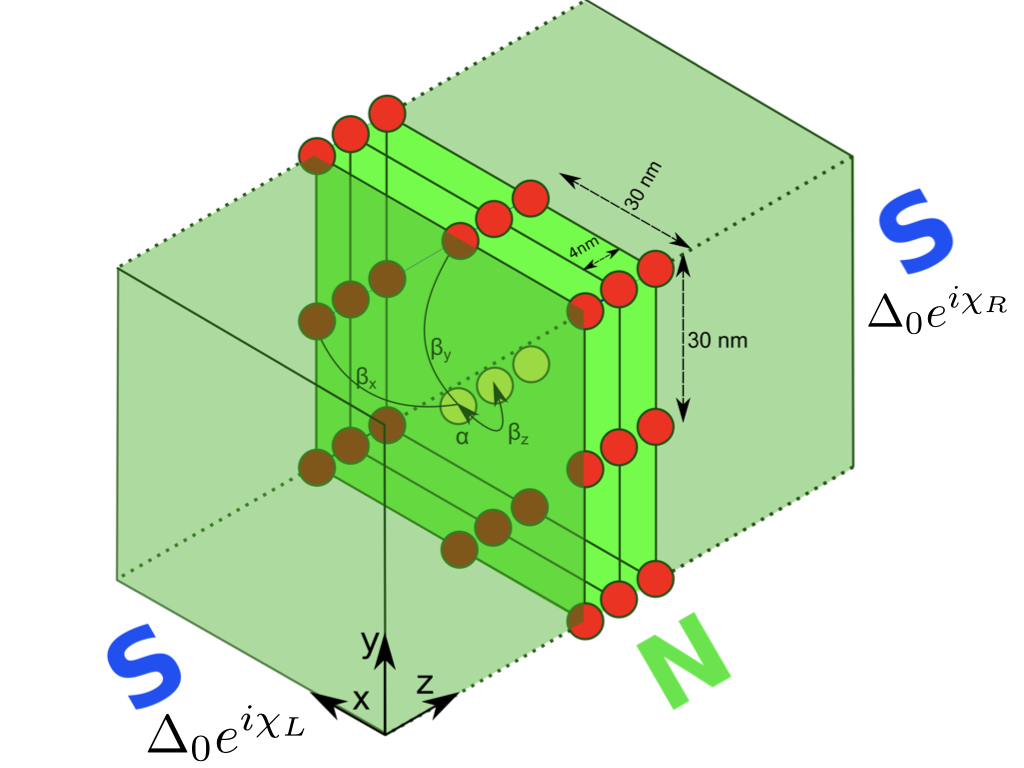
This paper is organised as follows. We start with the Bogoliubov-de Gennes mean-field description of a one-dimensional nanowire Josephson junction (SNS). In Sec. II, we describe the junction in a tight-binding model and outline the key aspects of the NEGF formalism. The details of this formalism have been relegated to Appendix A. Employing the NEGF formalism, we compute the Andreev bound state (ABS) spectrum and current phase relationship (CPR) for this junction. Previous work almost exclusively focused on the Andreev approximation regime, which assumes the chemical potential of the nanowire () to be much larger than the superconducting order parameter (), i.e., Beenakker 1992b; Bagwell 1992; Kulik 1969; Blonder et al. 1982. We go beyond this Andreev approximation limit and investigate the bound states which anti-cross at a superconducting phase difference of between the leads. This anti-crossing in the ABS is further analyzed in Appendix B. In Sec. III, we model three-dimensional Josephson junctions in a discrete lattice tight-binding model (Fig. 1). The radial confinement gives rise to transverse angular momentum subbands which pick up characteristic phases in a magnetic field. Section III.2 details the procedure we follow to label these angular momentum subbands. In Sec. IV, we reproduce the critical supercurrent oscillations in the presence of an axial magnetic field. Our results confirm these observed oscillations to be arising from the interference between orbital channels of the junction. With the aim of gaining a thorough understanding of the experiments, we consider scattering processes in the nanowire and study the effect of disorder, gate voltage fluctuations, and phase-breaking processes on the critical current oscillations.
II Formalism
Superconducting correlations are induced in a proximitised semiconductor by electron-hole conversions at the interface, a process known as Andreev reflectionAndreev 1964; Andreev 1967. Low bias transport in normal (N)-superconductor (S) junctions involves Andreev reflections at the interface.

We first consider a one-dimensional SNS junction consisting of a semiconductor nanowire with supercondcuting contacts. We model this system using the Bogoliubov-de Gennes (BdG) mean-field Hamiltonian within the tight-binding approximation, , where
| (1) | ||||
| (2) |
is the single-particle effective Hamiltonian, is the field operator with spin index , is the electron effective mass, and models a potential energy induced in the junction. The chemical potential is defined as the energy difference between the lowest occupied subband and the Fermi energy, and is denoted by . We assume an identical effective mass in the N and S regions thus neglecting the Fermi wave-vector mismatch at the interface. is the superconducting order parameter along the junction, which we assume to be constant with jump-discontinuities at the N/S interfaces
| (3) |
where is the unit step function at , is the superconducting phase of the left and right leads respectively, and is the phase difference. In the Nambu basis, we have the BdG equation
| (4) |
The device is divided into three parts – a normal semiconductor section with a length extended over , and semi-infinite superconducting contacts extending to on either side of the semiconductor (Fig. 2).

We discretise the continuum model of Eqs. 1, 2 into a lattice model with a spacing of . This is shown in Fig. 2. The superconductors are modelled as semi-infinite leads, while the number of lattice points in the normal region controls the length of the nanowire.
The on-site tight-binding parameters in the normal and superconducting regions, in the Nambu representation are
| (5) |
| (6) |
where, is the nearest neighbour tight binding hopping parameter. The hopping matrix is given by
| (7) |
This is not an atomic model, but an “effective” discrete lattice description of the junction. Parabolic dispersion relations correspond to the parameter space . Typical experiments are setup in the (Andreev approximation) regime. Hence, the choice of the effective lattice parameter is bound by the inequalities
| (8) |
The device Hamiltonian is subsequently written as
| (9) |
where is the creation operator of the Nambu spinor at site , and is the number of sites in the device. The Hamiltonian of the normal region can be written in the general form
| (10) |
II.1 Andreev bound states in SNS junctions
Andreev reflections at the N/S interfaces give rise to Andreev bound states in the semiconductor. We use the NEGF formalism to compute these bound state energies as a function of the superconducting phase difference () of the leads. The retarded Green’s function in the energy domain is given by
| (11) |
where denotes the energy, is the identity matrix and is an infinitesimal real constant. The Hamiltonian is given by Eq. 10. The self-energy terms model the coupling of the device to the semi-infinite leads. The self-energy is not hermitian, and its anti-hermitian part is responsible for the finite lifetime of the electron in the device. This subsequently contributes to broadening the energy levels in the device. The self-energies are computed using the surface-Green’s function, which requires an iterative procedure as outlined in Appendix A.
We compute the density of states () in the nanowire as the trace of the spectral Green’s function
| (12) |
The real-valued singularities of the density of states are the Andreev bound state (ABS) energies. This is computed as a function of the phase difference () of the order parameter of the contacts and is shown in Fig. 3. The parameters for this computation are consistent with the Andreev approximationAndreev 1964; Andreev 1967; Beenakker 1992b; Ashida et al. 1989 (). As discussed in Appendix B, the breakdown of this approximation is manifested as an avoided level crossing in the ABS spectrum.

II.2 Current phase relationship
The current-phase relationship (CPR) links the macroscopic current flow in the junction to the phase gradient of the superconducting order parameterJosephson 1962; Spanton et al. 2017. The traditional approach to computing the CPR involves a demarcation of the bound state and continuum currents. The bound state current involves transport in the sub-gap energy range () while the continuum current is supported by the continuous energy spectrum outside the gap. Once the ABS spectrum is computed from scattering theory, a thermodynamic relation is used to calculate the bound state current, and the transmission formalism is used for the continuum current. The total current is the sum of the bound state and continuum currentsKulik 1969.
By contrast, when using the NEGF formalism the current-energy density can be computed at contact , as a function of the phase difference using the current operatorDatta 1995; Datta 2005
| (13) |
where is the Fermi-Dirac occupation probability for a given energy level and is the Boltzmann constant. and are the retarded (advanced) Green’s function and contact self-energy respectively. To incorporate the opposite charge of electrons and holes we use the Pauli-z operator () in the particle-hole Nambu space. This current operator is reviewed in the Appendix A. The total current at a phase difference is then given by
| (14) |
Figures 4 and 4 compares the current phase-relations for a short () and long junction () respectively, as calculated from ideal scattering theory and NEGF. Here, is the healing length as defined in the following section (Eq. 22). By the term “ideal scattering theory” we refer to a scattering approach which explicitly neglects normal reflections at the N/S interface in a clean junctionKulik 1969; Bagwell 1992; Gharavi and Baugh 2015; Beenakker 1992b. With this assumption of no normal reflections, the bound states in a clean junction cross at . Hence, there’s a discontinuity at in the CPR calculated using this method. The NEGF result is expected to match scattering theory exactly in the limit.


III Transverse subbands in Josephson Junctions
We now consider a more realistic three-dimensional model of the junction with a magnetic field along the nanowire axis, parallel to the direction of current flow. Figure 1 illustrates a discrete lattice model of the three-dimensional nanowire. The junction is along the -direction and the transverse subbands are on the - plane. In III-V semiconductors (InAs, InN) the charge carriers are typically confined close to the surface due to a positive surface potential, forming a surface accumulation layer. In accordance with this, we use a shell conduction model by including a large surface confining potential at the core of the nanowire (yellow sites in Fig. 1). The radial confinement and azimuthal periodicity of the nanowire gives rise to transverse subbands.
The single-electron Hamiltonian of the nanowire is
| (15) |
where is the longitudinal direction, is the surface confinement potential, and is the Hamiltonian of the transverse modes.
For a cylindrical nanowire, the rotational symmetry about the longitudinal axis results in angular momentum subbands. This is because
| (16) |
where is the angular momentum operator in the z-direction. Hence, is a good quantum number. The subbands are eigenstates of the operator, labelled by their eigenvalue
| (17) |
We can consider the square cross-section in Fig. 1 as a perturbation to an ideal cylindrical geometry. Each of the transverse subbands in a square cross-section can be written as a superposition of angular momentum eigenstates. In Sec. III.2, we compute the average angular momentum of each transverse subband, and observe only a small difference (see Fig. 5) from the unperturbed quantized eigenvalues (). We will thus work within the zeroth order of this perturbation and use the language of angular momentum subbands in our analysis.
The azimuthal motion of the Andreev quasiparticles couples with the applied magnetic field, resulting in a quasiparticle phase pickup. Oscillations in the maximal supercurrent (critical current) with field have been measured by Gharavi et al. 2014, and Zuo et al. 2017. Unlike the Fraunhofer interference in wide planar junctions, the field is aligned with the current and the oscillations do not show any periodicity.
Using Peierls substitution, we include the orbital effect of the vector potential in the phase of the transverse hopping. For a constant magnetic field along the -direction, the vector potential can be written as
| (18) |
Within the tight-binding approximation, the on-site and hopping matrices in the particle-hole Nambu space are given by
| (19) |
where
| (20) |
| (21) |
where is the flux quanta per unit cell of the nanowire cross-section, and is the lattice site index in the direction. This factor alters the on-site energy () and contributes a phase to the hopping term corresponding to the gauge chosen for the vector potential (Eq. 18).
III.1 Andreev bound states in a magnetic field
Figures 5(a), and 5(b) plot the subgap density of states as obtained from the spectral Green’s function (Eq. 12) for a nanowire with an InAs effective mass = 0.023Nakwaski 1995 ( is the bare electron mass), radius R = 30 nm and chemical potential . As described in Appendix B, the bound states anti-cross at due to normal reflections at the N/S interfaces. A normalised flux of () is applied in Fig. 5(a) (Fig. 5(b)), which breaks symmetry in the transverse direction (Eq. 18) and lifts the degeneracy of the subbands. Here, , where is the cross-sectional area, and is the flux quantum.


The chemical potential is adjusted to populate three subbands. In Fig. 5 we see that the subband remains unaffected, while the subbands split in the presence of an axial flux. The splitting is proportional to the flux and the subband angular momentum. The process used to label the subbands is described in Sec. III.2.
The characteristic length-scale associated with an occupied subband is called the healing length Kulik 1969; Bagwell 1992, and is given by
| (22) |
is the fermi-velocity and is given by
| (23) |
We have a “short junction” when the nanowire is shorter than the healing length (). Note that the healing length depends on the angular momentum quantum number, and the classification of the junction as long/short is subband dependent.
We now describe a procedure to label the angular-momentum subbands using the correlation Green’s function ().
III.2 Average angular momentum of the transverse subbands
The angular momentum of the subbands can be computed as the expectation of the operator (Eq. 17), however, we do not have access to the wavefunctions in a numerical simulation. We do have the correlation Green’s function which gives the particle-hole density per-unit energy. Using this, we find the expectation of the operator as a function of energy
| (24) |
where returns the peak subgap quasiparticle concentration. In the Cartesian coordinate system, the operator is written as
| (25) |
The position operators are diagonal in the tight-binding basis, with each entry a multiple of the lattice constant (). For example, if we consider two points along the and axis, and one along , we have the following position operators
| (26) |
The linear momentum operators can be written as
| (27) |
where the subscript is used to denote basis of the position and momentum operators. Using Eq. 25, 26, 27, we write the operator and using Eq. 24 we find the expectation of as a function of energy.
We employ the above procedure to compute the average angular momentum of the Andreev bound states in an SNS junction. The chemical potential is fixed to give us three occupied subbands (). The average angular momentum of the subbands at , is shown in Fig. 5(c). Next, we increase the axial magnetic flux through the nanowire to . The subband states further split (Fig. 5(b)), and the angular momentum of the subbands is plotted in Fig. 5(d) for . The zero angular momentum subband () has no azimuthal motion, and hence is unaffected by the axial field. A non-zero for the subband (Figs. 5(c), 5(d)) results from its hybridisation with the nearby subband. This consequently decreases the magnitude for the subband w.r.t. .
From Figs. 5(c),5(d) we infer that each transverse subband is primarily composed of a single angular momentum eigenstate. This resemblance to the subband structure of an ideal cylindrical nanowire is the basis for Sec. III.4, where we build an effective subband model by including of a fixed number of angular momentum subbands. In the next section we explain the importance of including only the zero angular momentum subband in the superconducting contacts.
III.3 Zero angular momentum subband in the Superconductor
The BdG Hamiltonian in a superconductor is given by
| (28) |
For a cylindrical geometry with an azimuthal vector potential, is given by
| (29) |
As discussed, the radial confinement due to the nanowire’s cylindrical geometry gives rise to angular momentum subbands labelled by .
We will analyze the eigenenergies of this superconductor in the presence and absence of a magnetic field.
III.3.1 Zero magnetic field,
Using the ansatz wavefunction , the diagonal elements of the BdG Hamiltonian can be written as
where is the effective chemical potential
| (30) |
The BdG Hamiltonian simplifies to
| (31) |
and its eigenvalues are given by
| (32) |
This is the well-known superconductor dispersion relation, with a gap of on either side of the fermi level.
III.3.2 Constant axial magnetic field,
In the Coulomb gauge we can write the vector potential for this magnetic field as
| (33) |
From Stoke’s law
| (34) |
Exploiting the symmetry of the cylindrical geometry, the above equation can be simplified to
| (35) |
Using the same ansatz , the diagonal elements can be written as
| (36) |
| (37) |
for the electron and hole parts respectively. The effective chemical potential is defined in Eq. 30, and the field-coupling term . We note that
| (38) |
The BdG Hamiltonian can then be written as
| (39) |
and the eigenvalues are given by
| (40) |
Thus, we see that a magnetic field “shifts” the superconducting gap. It is no longer centred at the fermi level.


While this may be a good model for a superconducting “nanowire”, experimental setups usually involve a superconductor sputtered into quasi-planar contactsGharavi et al. 2014; Zuo et al. 2017 which naturally support only the subband. The geometry of the superconducting contacts implies a large subband energy, and can safely be assumed to remain unpopulated. This difference in geometry prompts the inclusion of subbands in the nanowire, and their exclusion in the superconductor.
For , we have , and thus the superconducting gap stays centered at the fermi level. This is illustrated in Fig. 6 – when subbands are included in the superconductor (Fig. 6(a)), the ABS move vertically as a result of the shift in the superconducting gap. However, with only the zero angular momentum subband in the superconductor (Fig. 6(b)), the ABS curves are horizontally phase shifted whilst the superconducting gap remains fixed. This shift is proportional to the applied flux, and the angular momentum of quasiparticles occupying the subband.
III.4 The 1-dimensional effective subband model
As outlined above, it is important to ensure that we only have the subbands in the contacts. We also note from Eqs. 30, 41 that we can incorporate the effect of the angular momentum subbands via an effective potential , and a field-coupling term .
The tight-binding Hamiltonian of the nanowire can be written as
| (43) |
| (44) |
| (45) |
| (46) |
where is the number of subbands. (For example, ()) and is the identity matrix.
Meanwhile, the Hamiltonian of the contacts takes a similar form with
| (47) |
IV Supercurrent Oscillations
IV.1 Clean junction
We compute the CPR of an SNS junction at finite axial magnetic fields, assuming a shell conduction model, and a nanowire diameter of 60 nm. Temperature is set to mK in all the simulations. In Fig. 7(b), we show the CPR as a function of the magnetic flux for a single occupied subband. With only the subband populated, there is no phase shift in the ABS, and the CPR retains its saw-tooth shape with a maximum near . The critical current as a function of the flux is plotted in Fig. 7(a). The gradual fall in the critical current can be attributed to the decrease in average quasiparticle momentum with increasing flux, as shown in Eq. 23. Eventually, at the band depopulates and the current falls to zero. We observe in Fig. 7(a) that the critical current does not monotonically decrease to zero, particularly for . The appearance of these small oscillations is due to the interference with the quasiparticles normally reflected from the N/S interfaces. As discussed in Appendix B, the discontinuity in the density of states gives rise to normal reflections. These reflected quasiparticles interfere and result in the non-monotonic decrease of the single subband critical current.


Next, we consider the case when three subbands are occupied (). The magnetic field evolution of the CPR is plotted in Fig. 8. Since the ABS for the subbands are phase shifted in presence of a flux (Fig. 6(b)), the total current is no longer maximum near . The current in the junction is the sum over the individual subband currents, and consequently, the flux-dependent phase shift results in an interference pattern for the field evolution of the critical current. The phase shift in a subband CPR is proportional to the difference in the electron-hole wavenumbers (Eq. 42), and the length of the junction. Hence, the fluxes at which the subband currents constructively interfere need not occur at integer multiples of the flux quantum .
In Fig. 8(a) we plot the critical current for three occupied subbands as a function of the axial flux. We see several oscillations of the critical current before the subbands depopulate at . At zero flux, the CPR of each subband is maximum near and hence they all add up constructively. As illustrated in Fig. 8(b), each subband contributes equally to the critical current.
As the flux is increased, the electron-hole pairs in the subbands pickup a phase and the subband CPRs no longer interfere constructively. Consequently, the critical current decreases with flux. At , the and subband CPRs are maximally out-of-phase, resulting in a local minima (node). The subband and total CPR at this node is plotted in Fig. 8(c). Beyond , the critical current switches phase from to and the current increases again. This increase persists till at which point the current is maximum near . At this flux, the subband current peaks near while it is negligible near . Hence, this secondary peak – which only involves contribution from subbands – is approximately a two-third of the primary peak and corresponds to a phase pickup of in the aforementioned subbands. The subband and total CPR for the secondary peak is shown in Fig. 8(d). As noted earlier, the magnitudes of the primary and secondary peaks progressively diminish due to the decrease in average quasiparticle velocity.


Finally, we consider the situation when five subbands are occupied (). The critical current is plotted as a function of the magnetic flux in Fig. 9. Once again, at the subband currents are all in-phase and constructively interfere to give a maximum. In presence of a magnetic field, the quasiparticles in the and subbands pick up different phases and hence, they do not appear to constructively interfere again in presence of a magnetic field to recover the zero field critical current.

The absence of such oscillations with a single occupied subband (Fig. 7(a)) confirms the subband supercurrent interference as the causal agent.
IV.2 Effect of disorder
In order to simulate experimentally relevant conditions, we include a random uncorrelated onsite disorder potential in the semiconductor. This models phase-coherent scattering events in the junction. We parameterise the disorder by the mean free path (), which is estimated from the disorder-averaged normal state conductance () using the following relation
| (48) |
is the number of subbands and is the length of the junction.
In Fig. 10 we plot the critical current oscillations in a nanowire for particular realisations of the disorder. While the initial decay and the oscillations are still present, the secondary maxima are suppressed. In a clean nanowire with a saw-tooth CPR (which peaks near at zero field), at a magnetic flux the subbands pickup a phase of and their CPRs peak near . The subband retains its sawtooth CPR with a negligible current near . As described in the previous subsection, this results in the secondary maximum. Upon adding disorder to the nanowire, we depart from this saw-tooth CPR, tending towards a sinusoidal CPR which peaks further away from at zero field. Thus, there exists no at which the subband current peaks while the subband current is negligible. As a consequence of the sinusoidal CPR, on picking up a phase of the subbands destructively interfere with the subband, and this causes the suppression of the secondary maxima.


In the presence of scatterers the effective path traversed by the quasiparticles increases and hence, the subbands destructively interfere at a lower flux. This is shown in Fig. 11, where the first crticial current node in a disordered junction occurs at a lower field as compared to the clean nanowire.

Furthermore, as shown by Zuo et al. 2017, the essential effect of disorder can be observed by the dependence of the critical current oscillations on the gate voltage. As shown in Fig. 12(a) for the clean nanowire, small variations in the gate voltage hardly cause any fluctuations in the oscillations. This is because small changes in the chemical potential do not change the number of occupied subbands and only weakly affects the quasiparticle transmission through the junction. However, in a disordered nanowire with a small mean free path, the quasiparticles traverse a longer path in the nanowire and hence, the critical current oscillations are significantly affected by the gate voltage. This is shown in Figs. 12(b),12(c) for two disorder realisations.
From Figs. 10,12 we infer that the critical current oscillations are highly sensitive to the gate voltage and the particular realisation of the disorder. Thus, a macroscopic current measurement indirectly gives us information about the microscopic specifics of the junction. However, while our model provides a qualitative understanding of the oscillations, the high sensitivity w.r.t. the microscopic parameters renders a quantitative description of the experiment highly challenging.


IV.3 Dephasing in the nanowire
The analysis presented in the previous sections described the phase-coherent flow of quasiparticles in the junction. We now include phase-breaking processes Golizadeh-Mojarad and Datta 2007; Datta 2005 that may arise from any time-dependent potential, such as the interaction of an electron with the surrounding bath of phonons, other electrons, or fast-fluctuating charge noise caused by traps in defects. Although it is non-trivial to identify the dominant source of dephasing, we can adopt a phenomenological model by introducing a Büttiker probe for the lattice backgroundDatta 2005.
We subsume these processes within the NEGF formalism by including a self-energy term for the lattice background , proportional to the Green’s function and the emission-absorption coefficients. This calls for a self-consistent computation of the Green’s function and the bath self-energy Golizadeh-Mojarad and Datta 2007
| (49) | ||||
| (50) |
where denotes element by element multiplication. The elements of the matrix represent the correlation of the time-dependent interaction potential between pairs of lattice points. Adopting a homogeneous model, we assume uniform, elastic, and spatially uncorrelated interactions resulting in a diagonal ,
| (51) |
for every pair of coordinates and in the nanowire. This model discards the off-diagonal elements of the Green’s function, and hence relaxes both the phase and momentum of the quasiparticles in the nanowire.
The magnitude of limits the phase relaxation length of the junction. Molecular beam epitaxy(MBE) and metalorganic vapour phase epitaxy grown InAs nanowires typically have a phase relaxation length on the order of a few-hundred nanometers nmBlömers et al. 2011b; Estévez Hernández et al. 2010b; Doh et al. 2007. In our model, can be estimated from the statistical properties of universal conductance fluctuations (UCF)Blömers et al. 2011b; Estévez Hernández et al. 2010b; Doh et al. 2007 The details of this calculation is presented in Appendix D, and the results are tabulated here in Table 1
| (eV2) | (nm) |
|---|---|
| 247 | |
| 157 | |
| 105 |
The critical current oscillations in the presence of elastic dephasing interactions, as listed in Table 1, are shown in Fig. 13. The green curve in Fig. 13 includes a random disorder potential profile in addition to the phase-breaking processes. With dephasing in the nanowire, the excess path traversed due to the disorder potentials does not result in a proportionate phase pick-up. Consequently, in contrast to Fig. 11, the inclusion of disorder does not result in a significant shift in the critical current nodes.
One of the main effects of dephasing is in pinning down the critical current nodes so that they’re less sensitive to disorder. A phase-coherent simulation would overestimate the disorder-induced quasiparticle phase pickup and consequently, the computed critical current oscillations are sensitive and strongly dependent on the microscopic disorder profile (see Fig. 10). However, measured oscillations from Zuo et al. 2017 exhibit only a gradual variation in the oscillations with changing disorder realizations – well modeled by the inclusion of dephasing in the nanowire. Further, dephasing is necessary to reproduce the observed reduction of the relative peak height for subsequent primary maxima. Phase-breaking processes restrict the coherent life time of the quasiparticles in the nanowire, which hinders a constructive interference at higher fields. This is well illustrated in Fig. 13, where the relative peak height of the second primary maximum (third peak) decreases with an increase in dephasing strength.
Magnetoconductance calculations by Lahiri et al. 2018 reveal the suppression of higher harmonics of the transmission characteristics in a nanowire with dephasing. This is manifest in experiments as an increasing inter-node spacingZuo et al. 2017; Gharavi et al. 2014 with respect to the axial field. As illustrated in Fig. 13, this feature is captured by the inclusion of phase-breaking processes in our model. The oscillations in Fig. 13 are in good qualitative agreement with the experiments by Gharavi et al. 2014 and Zuo et al. 2017. Thus, we infer that phase-breaking processes play a non-negligible role in III-V semiconductor nanowire Josephson junctions.


V Conclusion
In this paper we employed the Keldysh Non-Equilibrium Green’s Function formalism to model quantum transport in semiconductor nanowire Josephson junctions. In our analysis we used a three-dimensional discrete lattice model described by the Bogoliubov-de Gennes Hamiltonian in the tight-binding approximation, and computed the Andreev bound state spectrum and current-phase relations. We went beyond the Andreev approximation limit and investigated the avoided level crossing in the ABS spectrum. Our results confirm the measured critical current oscillations to arise from the subband supercurrent interference in presence of an axial magnetic field. The phase picked up by the quasiparticles depend on the difference of their wavenumbers, the length of the junction and the angular momentum quantum number. Thus, the oscillations do not show any periodicity in the flux quantum through the nanowire cross-section. We included phase-coherent scattering to model a disordered junction and investigated its effect on the critical current oscillations. We observed that the oscillations in the disordered junction are highly sensitive to the realisation of the random disorder potential, and on small fluctuations of the gate voltage. This high sensitivity makes a quantitative description of the experiment a challenging task. Nevertheless, a macroscopic current measurement conveys valuable information about the microscopic profile of the junction. We include elastic dephasing in the nanowire by modelling weak phase-breaking interactions. A good qualitative match of our results with the experiment is observed, and this underscores the role played by phase-breaking processes in III-V nanowire Josephson junctions.
The relevance of these results is emphasized by outlining the points of comparison with experimental data from Gharavi et al. 2014 and Zuo et al. 2017. The data exhibits a strong suppression of the switching current at magnetic fields on the order of . Subsequently, oscillations with aperiodic nodes are observed in the field dependence of the switching current. As shown in Fig. 13, our simulations capture the characteristic features of this evolution. Furthermore, as observed in the experiments, the simulated oscillations display a strong gate-tunability and are not uniquely determined by the junction geometry. Finally, a phase-coherence length in the range nm of MBEBlömers et al. 2011b and metalorganic vapor phase epitaxyEstévez Hernández et al. 2010b; Doh et al. 2007 grown InAs nanowire samples corroborates the dephasing in our model, as introduced by a uniform, spatially uncorrelated dephasing parameter .
Acknowledgements: The authors BM and PS would like to thank Prof. Supriyo Datta, Prof. Kantimay Das Gupta, Abhishek Sharma and Aritra Lahiri for useful discussions throughout this work. This work is an outcome of the Research and Development work undertaken in the project under the Visvesvaraya PhD Scheme of Ministry of Electronics and Information Technology, Government of India, being implemented by Digital India Corporation (formerly Media Lab Asia). This work was also supported by the Science and Engineering Research Board (SERB) of the Government of India under Grant number EMR/2017/002853. KG and JB acknowledge funding from the Natural Sciences and Engineering Research Council of Canada (NSERC).
Appendix A Non Equilibrium Green’s Function Formalism (NEGF)
The retarded Green’s function in the energy domain is given by
| (52) |
where is the Hamiltonian, are the retarded self-energies of the semi-infinite contacts, and is an infinitesimal real constant. The advanced Green’s function is the Hermitian conjugate of the retarded Green’s function (). The Hamiltonian is written in the tight-binding approximation Eq. 10. The surface Green’s functions () at each contact are recursively evaluated
| (53) | ||||
| (54) |
where the subscript labels the contact. Using this we compute the self-energy
| (55) |
where , and
The anti-Hermitian part of the self-energy is responsible for the finite life-time of the quasiparticles in the junction and broadens the energy levels. This broadening matrix is denoted by .
The Fermi functions in the particle-hole Nambu space is given by
| (56) |
where is the fermi function, and is the bias applied to the contact.
The lesser self-energy, or the inscattering matrix can be computed from the broadening matrix and fermi function as
| (57) |
The lesser Green’s Function is then computed
| (58) |
Next, we construct the current operator
| (59) | ||||
| (60) |
Electrons and holes travelling in the same direction carry opposite currents and hence, the current is given by the difference of the partial trace of the current operator over the electron and hole sub-spaces.
| (61) |
This can be also be written as
| (62) |
where is the Pauli operator in the particle-hole Nambu space. The total current is then evaluated by integrating the current-energy density
| (63) |
There’s a small technical caveat to keep in mind when using the NEGF current operator.
Using the equations for the retarded and advanced Green’s functions,
where
Pre-multiplying by and post-multiplying by ,
| (64) | ||||
| (65) | ||||
| (66) |
Multiplying the fermi-function,
| (67) |
Thus,
| (68) |
However, if we don’t consider the term proportional to the infinitesimal we end up with
| (69) |
from Eq. 69 misses a term in the current proportional to , the trace of which increases with the number of bound-states. This leads to erroneous results for longer nanowires, which have a larger number of Andreev Bound States. The NEGF current-operator for contact is given by –
| (70) |
Substituting and , the current operator can be simplified to
| (71) |
Appendix B Andreev bound state spectrum : Beyond Andreev approximation
Andreev reflections across an N/S interface were first analyzed by Blonder et al. 1982 in 1982, and have been prevalent in the literature ever since. Almost always, these results are derived under the Andreev approximationAndreev 1964; Andreev 1967; Beenakker 1992b; Ashida et al. 1989. This approximation deals with a regime where the chemical potential of the nanowire is much larger than the superconducting order parameter of the leads (). In this appendix, we analyze the implications of working in a regime where the Andreev approximation is not valid. Specifically, we consider the implications of being outside the Andreev approximation regime on the ABS spectrum in a clean 1-dimensional SNS junction.
The density of states in a superconductor is gapped by an energy on either side of the fermi level. There is no gap in the normal state spectrum. Thus, quasiparticles in the subgap region face an energy barrier at the interface. This is an energy barrier between states with the same momentum, arising due to a difference in the order parameter () across the interface. This has nothing do with an impurity or any non-ideality of the junction. However, it plays a role very similar to any impurity-induced barrier at the interface, i.e. it gives rise to normal reflections at the interfaces, which cannot be neglected when is not valid, even for a clean junction.
We now examine the spectrum for the chemical potential comparable to . Figure. 14 plots the ABS spectrum for .

We observe an avoided level crossing when , as shown in Fig. 14. This anti-crossing can be attributed to the normal reflections which become significant in this parameter space. When these normal reflections are negligible, we have independent rightward and leftward moving excitations in the nanowire, resulting in a crossing at . However, once normal reflections become important, as is the case outside the Andreev approximation, the excitations moving in opposite directions get coupled to each other. This interaction between them, brought about by the normal reflections at the N/S interfaces, results in the anti-crossing.
In Fig. 15, we plot the ABS energy gap () at as a function of . It is evident from this plot that decreases as increases. Thus, in the Andreev approximation regime () the bound states cross () at . When is kept constant and is varied, the gap varies as for . In Appendix C we verify this dependence analytically by taking a scattering theory approach. Figure 15 plots the variation of the gap at with the nanowire length. These oscillations result from the interference of the waves reflected at the two S/N interfaces.


Appendix C The Andreev bound state quantisation condition outside the Andreev Approximation Regime
In this appendix we derive an expression for the Andreev bound state energy in a SNS junction, when the phase difference between the two superconductors is tuned to . We show this to be non-zero for a finite while approaching zero in the limit , where is the chemical potential of the entire device and is the induced superconducting gap.
C.1 Setting up the problem
We follow the notation from Kulik 1969. Consider first the transport of an electron across an N/S interface. It is well known that for a clean interface, an incident electron is perfectly Andreev reflected as a hole. However, there is also a component of the order which is reflected as a normal electron. This is mentioned in Kulik 1969’s work and can also be derived from first principles scattering theory at the N/S interface. We usually encounter cases when perfect Andreev reflection is assumed with no normal reflectionAndreev 1964; Andreev 1967; Beenakker 1992b; Ashida et al. 1989, but this is only true to the zeroth order in .
This normal reflection component will modify the Andreev bound state quantization conditionGharavi and Baugh 2015; Kulik 1969
| (72) |
where , and are the electron and hole wave vectors and is the phase difference between the superconducting order parameter across the junction.
Consider an SNS junction with a normal region length extended over , and superconducting contacts defined over . Writing the two-component wave functions
| (73) |
The terms proportional to , and are ignored when perfect Andreev reflection is assumed. We have included a coefficient to emphasize a first order expansion beyond the perfect Andreev reflection scenario.
Equating the coefficients at , we get:
| (74) | ||||
| (75) | ||||
| (76) | ||||
| (77) |
Solving for and (to be compared with Eq 2.13 from Kulik 1969), we get:
| (78) |
| (79) |
We now divide the above equations and keep terms to first order in ,
| (80) |
We will now focus on the qualitative behaviour of the solutions of the above equation. In order to do so, we simplify the above equation into a more tractable form:
| (81) |
where the exact form of and can be derived from equation 80.
C.2 Expression for the energy at
Let us tune the phase difference . Defining , we can write . Using this relation, the quantization condition can be simplified to,
| (82) |
Equating the real and imaginary parts,
| (83) | ||||
| (84) |
Since , under the small angle approximation Eq. 84 can be simplified to
| (85) |
For
| (86) |
This can be further simplified using ,
| (87) |
| (88) |
This is a finite energy for non-zero and goes to zero in the limit .
C.3 Comparison with numerics
Ignoring the term in the bracket from the final expression for E, we can simplify it to . We decided to observe the power law dependence of the gap using the numerical simulations. We considered two cases:
- 1.
Fix and vary : we expect to see a behavior
(89) - 2.
Fix and vary : we expect to see a behavior
(90)
Figure 16 confirms this dependence of the ABS energy on for the aforementioned cases.


Appendix D Phase relaxation length estimation
The dephasing in the nanowire can be parameterised by the phase relaxation length , which is a length scale over which the phase of the quasiparticles randomise. As explained in Sec. IV.3, phase-breaking processes are included via a self-energy for the lattice background ; . In this appendix, we estimate as a function of the dephasing strength .
D.1 Estimation from phase coherence lifetime
The phase relaxation length can be computed from the phase coherence lifetime
| (91) |
where is the Fermi-velocity, and is the diffusion constant. The anti-hermitian part of the lattice background self-energy limits the phase-coherent lifetime of the quasiparticles, and sets an energy scale for the problem. The phase coherence lifetime can thus be estimated as
| (92) |
where is a diagonal element of is the broadening function corresponding to the lattice background. Note that , and hence the so estimated from Eq. 91 is a function of energy. The phase relaxation length is then reported as an average over the energy grid, . Under the assumption of ballistic transport, we estimate an upper bound on the phase relaxation length nm for eV2, and for eV2, nm. The Fermi-velocity decreases with field, and hence we observe a gradual monotonic degradation in the phase relaxation length.


D.2 Estimation from statistical properties of UCF
For a nanowire length comparable to , the normal-state conductance fluctuates with an amplitude of the order of in presence of a magnetic field. These aperiodic universal conductance fluctuations (UCF) measured in a magnetic field perpendicular to the nanowire axis can be analysed to extract information on phase coherent transport. The UCF originates from electron phase shifts resulting from the penetration of magnetic flux through closed electron trajectories. The conductance shows strong fluctuations for low dephasing strengths, while they are smeared out at higher coupling strengths.
The magnetoconductance fluctuation is denoted by
| (93) |
where the average is taken over the magnetic field . The average fluctuation amplitude about the mean conductance is quantified by the root-mean-square . The rms decreases monotonically with . The phase relaxation length can be estimated from the analysis of the autocorrelation function of . The half-width half-maximum (HWHM) of corresponds to the correlation field , which is a measure of a field range over which the phases of the interference path become uncorrelated.
| (94) | ||||
| (95) |
Assuming the phase relaxation length to be greater than the nanowire diameter , we can extract directly from the correlation fieldBlömers et al. 2011b; Estévez Hernández et al. 2010b; Beenakker and van Houten 1988
| (96) |
where is a dimensionless prefactor depending on the transport regime. We work in the the dirty metal limit with Blömers et al. 2011b.
D.2.1 Results
This simulation involves normal-state low-bias transport in presence of a magnetic field oriented in a direction perpendicular to the nanowire axis. The nanowire length nm, and diameter nm. To model diffusive transport, an onsite random potential in the range is introduced at each point in the nanowire, where is the tight-binding hopping parameter. This corresponds to a mean-free path nm. The magnetoconductance fluctuations are plotted in Fig. 18(a). The normalised autocorrelation of is shown in Fig. 18(b), and the extracted parameters are listed in Table 2.


| (eV2) | rms() | (nm) | |
|---|---|---|---|
| 0.038 | 0.56 | 247 | |
| 0.0048 | 0.88 | 157 | |
| 0.00098 | 1.32 | 105 |
References
- Zhang et al. (2018) H. Zhang, C.-X. Liu, S. Gazibegovic, D. Xu, J. A. Logan, G. Wang, N. van Loo, J. D. S. Bommer, M. W. A. de Moor, D. Car, R. L. M. Op het Veld, P. J. van Veldhoven, S. Koelling, M. A. Verheijen, M. Pendharkar, D. J. Pennachio, B. Shojaei, J. S. Lee, C. J. Palmstrøm, E. P. A. M. Bakkers, S. D. Sarma, and L. P. Kouwenhoven, Nature 556, 74 EP (2018).
- Mourik et al. (2012) V. Mourik, K. Zuo, S. M. Frolov, S. R. Plissard, E. P. A. M. Bakkers, and L. P. Kouwenhoven, Science 336, 1003 (2012), http://science.sciencemag.org/content/336/6084/1003.full.pdf .
- Deng et al. (2016) M. T. Deng, S. Vaitiekenas, E. B. Hansen, J. Danon, M. Leijnse, K. Flensberg, J. Nygård, P. Krogstrup, and C. M. Marcus, Science 354, 1557 (2016), http://science.sciencemag.org/content/354/6319/1557.full.pdf .
- Chen et al. (2017) J. Chen, P. Yu, J. Stenger, M. Hocevar, D. Car, S. R. Plissard, E. P. A. M. Bakkers, T. D. Stanescu, and S. M. Frolov, Science Advances 3 (2017), 10.1126/sciadv.1701476, http://advances.sciencemag.org/content/3/9/e1701476.full.pdf .
- Das et al. (2012) A. Das, Y. Ronen, Y. Most, Y. Oreg, M. Heiblum, and H. Shtrikman, Nature Physics 8, 887 EP (2012).
- Rokhinson et al. (2012) L. P. Rokhinson, X. Liu, and J. K. Furdyna, Nature Physics 8, 795 EP (2012).
- Nayak et al. (2008) C. Nayak, S. H. Simon, A. Stern, M. Freedman, and S. Das Sarma, Rev. Mod. Phys. 80, 1083 (2008).
- Majorana and Maiani (2006) E. Majorana and L. Maiani, “A symmetric theory of electrons and positrons,” in Ettore Majorana Scientific Papers: On occasion of the centenary of his birth, edited by G. F. Bassani (Springer Berlin Heidelberg, Berlin, Heidelberg, 2006) pp. 201–233.
- Kitaev (2001) A. Y. Kitaev, Physics-Uspekhi 44, 131 (2001).
- Beenakker (2013) C. Beenakker, Annual Review of Condensed Matter Physics 4, 113 (2013), https://doi.org/10.1146/annurev-conmatphys-030212-184337 .
- Sau et al. (2010a) J. D. Sau, R. M. Lutchyn, S. Tewari, and S. Das Sarma, Phys. Rev. Lett. 104, 040502 (2010a).
- Sau et al. (2010b) J. D. Sau, S. Tewari, R. M. Lutchyn, T. D. Stanescu, and S. Das Sarma, Phys. Rev. B 82, 214509 (2010b).
- Alicea (2010) J. Alicea, Phys. Rev. B 81, 125318 (2010).
- Alicea (2012) J. Alicea, Reports on Progress in Physics 75, 076501 (2012).
- Lutchyn et al. (2010) R. M. Lutchyn, J. D. Sau, and S. Das Sarma, Phys. Rev. Lett. 105, 077001 (2010).
- Wimmer et al. (2011) M. Wimmer, A. R. Akhmerov, J. P. Dahlhaus, and C. W. J. Beenakker, New Journal of Physics 13, 053016 (2011).
- Alicea et al. (2011) J. Alicea, Y. Oreg, G. Refael, F. von Oppen, and M. P. A. Fisher, Nature Physics 7, 412 EP (2011).
- Sarma et al. (2015) S. D. Sarma, M. Freedman, and C. Nayak, Npj Quantum Information 1, 15001 EP (2015).
- Aasen et al. (2016) D. Aasen, M. Hell, R. V. Mishmash, A. Higginbotham, J. Danon, M. Leijnse, T. S. Jespersen, J. A. Folk, C. M. Marcus, K. Flensberg, and J. Alicea, Phys. Rev. X 6, 031016 (2016).
- Hyart et al. (2013) T. Hyart, B. van Heck, I. C. Fulga, M. Burrello, A. R. Akhmerov, and C. W. J. Beenakker, Phys. Rev. B 88, 035121 (2013).
- Karzig et al. (2017) T. Karzig, C. Knapp, R. M. Lutchyn, P. Bonderson, M. B. Hastings, C. Nayak, J. Alicea, K. Flensberg, S. Plugge, Y. Oreg, C. M. Marcus, and M. H. Freedman, Phys. Rev. B 95, 235305 (2017).
- Plugge et al. (2017) S. Plugge, A. Rasmussen, R. Egger, and K. Flensberg, New Journal of Physics 19, 012001 (2017).
- Stenger et al. (2019) J. P. T. Stenger, M. Hatridge, S. M. Frolov, and D. Pekker, Phys. Rev. B 99, 035307 (2019).
- Larsen et al. (2015) T. W. Larsen, K. D. Petersson, F. Kuemmeth, T. S. Jespersen, P. Krogstrup, J. Nygård, and C. M. Marcus, Phys. Rev. Lett. 115, 127001 (2015).
- de Lange et al. (2015) G. de Lange, B. van Heck, A. Bruno, D. J. van Woerkom, A. Geresdi, S. R. Plissard, E. P. A. M. Bakkers, A. R. Akhmerov, and L. DiCarlo, Phys. Rev. Lett. 115, 127002 (2015).
- Hassler et al. (2011) F. Hassler, A. R. Akhmerov, and C. W. J. Beenakker, New Journal of Physics 13, 095004 (2011).
- Kringhøj et al. (2018) A. Kringhøj, L. Casparis, M. Hell, T. W. Larsen, F. Kuemmeth, M. Leijnse, K. Flensberg, P. Krogstrup, J. Nygård, K. D. Petersson, and C. M. Marcus, Phys. Rev. B 97, 060508(R) (2018).
- Casparis et al. (2018) L. Casparis, M. R. Connolly, M. Kjaergaard, N. J. Pearson, A. Kringhøj, T. W. Larsen, F. Kuemmeth, T. Wang, C. Thomas, S. Gronin, G. C. Gardner, M. J. Manfra, C. M. Marcus, and K. D. Petersson, Nature Nanotechnology 13, 915 (2018).
- Estévez Hernández et al. (2010a) S. Estévez Hernández, M. Akabori, K. Sladek, C. Volk, S. Alagha, H. Hardtdegen, M. G. Pala, N. Demarina, D. Grützmacher, and T. Schäpers, Phys. Rev. B 82, 235303 (2010a).
- Blömers et al. (2011a) C. Blömers, M. I. Lepsa, M. Luysberg, D. Grützmacher, H. Lüth, and T. Schäpers, Nano Letters, Nano Letters 11, 3550 (2011a).
- Lahiri et al. (2018) A. Lahiri, K. Gharavi, J. Baugh, and B. Muralidharan, Phys. Rev. B 98, 125417 (2018).
- Cayao et al. (2015) J. Cayao, E. Prada, P. San-Jose, and R. Aguado, Phys. Rev. B 91, 024514 (2015).
- Lim et al. (2011) J. S. Lim, R. López, and R. Aguado, Phys. Rev. Lett. 107, 196801 (2011).
- Gharavi et al. (2014) K. Gharavi, G. W. Holloway, C. M. Haapamaki, M. H. Ansari, M. Muhammad, R. R. LaPierre, and J. Baugh, (2014), arXiv:1405.7455 [cond-mat.mes-hall] .
- Zuo et al. (2017) K. Zuo, V. Mourik, D. B. Szombati, B. Nijholt, D. J. van Woerkom, A. Geresdi, J. Chen, V. P. Ostroukh, A. R. Akhmerov, S. R. Plissard, D. Car, E. P. A. M. Bakkers, D. I. Pikulin, L. P. Kouwenhoven, and S. M. Frolov, Phys. Rev. Lett. 119, 187704 (2017).
- Szombati (2017) D. Szombati, doctoral thesis 1, 93 (2017).
- Keldysh (1964) L. V. Keldysh, Zh. Eksp. Teor. Fiz. 47, 1515 (1964), [Sov. Phys. JETP20,1018(1965)].
- Datta (1995) S. Datta, Electronic Transport in Mesoscopic Systems, Cambridge Studies in Semiconductor Physics and Microelectronic Engineering (Cambridge University Press, 1995).
- Datta (2005) S. Datta, “Atom to transistor,” in Quantum Transport: Atom to Transistor (Cambridge University Press, 2005) p. 285?311.
- DuBois (1967) D. DuBois, in Lectures in Theoretical Physics, Vol. 9C, edited by W. Brittin (Gordon and Breach, New York, 1967) pp. 469–620.
- Rammer and Smith (1986) J. Rammer and H. Smith, Rev. Mod. Phys. 58, 323 (1986).
- Zeng et al. (2003) Z. Y. Zeng, B. Li, and F. Claro, Phys. Rev. B 68, 115319 (2003).
- Cayao et al. (2017) J. Cayao, P. San-Jose, A. M. Black-Schaffer, R. Aguado, and E. Prada, Phys. Rev. B 96, 205425 (2017).
- San-Jose et al. (2013) P. San-Jose, J. Cayao, E. Prada, and R. Aguado, New Journal of Physics 15, 075019 (2013).
- Cayao et al. (2018) J. Cayao, A. M. Black-Schaffer, E. Prada, and R. Aguado, Beilstein Journal of Nanotechnology 9, 1339 (2018).
- San-Jose et al. (2014) P. San-Jose, E. Prada, and R. Aguado, Phys. Rev. Lett. 112, 137001 (2014).
- Beenakker and van Houten (1991) C. Beenakker and H. van Houten, in Semiconductor Heterostructures and Nanostructures, Solid State Physics, Vol. 44, edited by H. Ehrenreich and D. Turnbull (Academic Press, 1991) pp. 1 – 228.
- Singha et al. (2017) A. Singha, M. H. Fauzi, Y. Hirayama, and B. Muralidharan, Phys. Rev. B 95, 115416 (2017).
- De Gennes (1999) P. G. De Gennes, Superconductivity of Metals and Alloys, Advanced book classics (Perseus, Cambridge, MA, 1999).
- Tinkham (2004) M. Tinkham, Introduction to Superconductivity: Second Edition (Dover Books on Physics) (Vol i), second edition ed. (Dover Publications, 2004).
- Blonder et al. (1982) G. E. Blonder, M. Tinkham, and T. M. Klapwijk, Phys. Rev. B 25, 4515 (1982).
- Beenakker (1992a) C. W. J. Beenakker, Phys. Rev. B 46, 12841 (1992a).
- Gharavi and Baugh (2015) K. Gharavi and J. Baugh, Phys. Rev. B 91, 245436 (2015).
- Bagwell (1992) P. F. Bagwell, Phys. Rev. B 46, 12573 (1992).
- Groth et al. (2014) C. W. Groth, M. Wimmer, A. R. Akhmerov, and X. Waintal, New Journal of Physics 16, 063065 (2014).
- Levy Yeyati et al. (1995) A. Levy Yeyati, A. Martín-Rodero, and F. J. García-Vidal, Phys. Rev. B 51, 3743 (1995).
- Martín-Rodero et al. (1994) A. Martín-Rodero, F. J. García-Vidal, and A. Levy Yeyati, Phys. Rev. Lett. 72, 554 (1994).
- Beenakker (1992b) C. W. J. Beenakker, in Transport Phenomena in Mesoscopic Systems, edited by H. Fukuyama and T. Ando (Springer Berlin Heidelberg, Berlin, Heidelberg, 1992) pp. 235–253.
- Kulik (1969) I. O. Kulik, Soviet Journal of Experimental and Theoretical Physics 30, 944 (1969).
- Andreev (1964) A. F. Andreev, SOVIET PHYSICS JETP-USSR 19, 1228 (1964).
- Andreev (1967) A. F. Andreev, SOVIET PHYSICS JETP-USSR 24, 1019 (1967).
- Ashida et al. (1989) M. Ashida, S. Aoyama, J. Hara, and K. Nagai, Phys. Rev. B 40, 8673 (1989).
- Josephson (1962) B. Josephson, Physics Letters 1, 251 (1962).
- Spanton et al. (2017) E. M. Spanton, M. Deng, S. Vaitiekėnas, P. Krogstrup, J. Nygård, C. M. Marcus, and K. A. Moler, Nature Physics 13, 1177 EP (2017).
- Nakwaski (1995) W. Nakwaski, Physica B: Condensed Matter 210, 1 (1995).
- Golizadeh-Mojarad and Datta (2007) R. Golizadeh-Mojarad and S. Datta, Phys. Rev. B 75, 081301(R) (2007).
- Blömers et al. (2011b) C. Blömers, M. I. Lepsa, M. Luysberg, D. Grützmacher, H. Lüth, and T. Schäpers, Nano Letters 11, 3550 (2011b), pMID: 21848307, https://doi.org/10.1021/nl201102a .
- Estévez Hernández et al. (2010b) S. Estévez Hernández, M. Akabori, K. Sladek, C. Volk, S. Alagha, H. Hardtdegen, M. G. Pala, N. Demarina, D. Grützmacher, and T. Schäpers, Phys. Rev. B 82, 235303 (2010b).
- Doh et al. (2007) Y.-J. Doh, A. L. Roest, E. P. A. M. Bakkers, S. D. Franceschi, and L. P. Kouwenhoven, (2007), arXiv:0712.4298 .
- Beenakker and van Houten (1988) C. W. J. Beenakker and H. van Houten, Phys. Rev. B 37, 6544 (1988).