subsecref name = \RSsectxt \RS@ifundefinedthmref name = theorem \RS@ifundefinedlemref name = lemma
Theory of Ferroelectric ZrO2 Monolayers on Si
Abstract
We use density functional theory and Monte Carlo lattice simulations to investigate the structure of ZrO2 monolayers on Si(001). Recently, we have reported on the experimental growth of amorphous ZrO2 monolayers on silicon and their ferroelectric properties, marking the achievement of the thinnest possible ferroelectric oxide [M. Dogan et al. Nano Lett., 18 (1) (2018) (Dogan et al. 2018)]. Here, we first describe the rich landscape of atomic configurations of monocrystalline ZrO2 monolayers on Si and determine the local energy minima. Because of the multitude of low-energy configurations we find, we consider the coexistence of finite-sized regions of different configurations. We create a simple nearest-neighbor lattice model with parameters extracted from DFT calculations, and solve it numerically using a cluster Monte Carlo algorithm. Our results suggest that up to room temperature, the ZrO2 monolayer consists of small domains of two low-energy configurations with opposite ferroelectric polarization. This explains the observed ferroelectric behavior in the experimental films as a collection of crystalline regions, which are a few nanometers in size, being switched with the application of an external electric field.
I Introduction
Thin films of metal oxides have been a focus area of continuous research due to the rich physics that can be observed in these systems, such as ferroelectricity, ferromagnetism and superconductivity, and their resulting technological applications (Hwang et al. 2012; Mannhart and Schlom 2010). An important challenge involving thin metal oxide films has been their growth on semiconductors in such a way that their electrical polarization couples to the electronic states inside the semiconductor (Reiner et al. 2009; Reiner et al. 2010; Dogan and Ismail-Beigi 2017). If successfully done, this enables the development of non-volatile devices such as ferroelectric field-effect transistors (FEFET). In a FEFET, the polarization of the oxide encodes the state of the device, and requires the application of a gate voltage only for switching the state, greatly reducing the power consumption and boosting the speed of the device (McKee et al. 2001; Garrity et al. 2012). Meeting this challenge requires a thin film ferroelectric oxide, as well as an atomically abrupt interface between the oxide and the semiconductor, so that the polarization of the oxide and the electronic states in the semiconductor are coupled. The first of these requirements, i.e., a thin film ferroelectric, is difficult to obtain because materials that are ferroelectric in the bulk lose their macroscopic polarization below a critical thickness, due to the depolarizing field created by surface bound charges (Batra et al. 1973; Dubourdieu et al. 2013). An alternative approach is to search for materials such that, regardless of their bulk properties, they are stable in multiple polarization configurations as thin films (Dogan and Ismail-Beigi 2017). The second requirement, i.e., an abrupt oxide-semiconductor interface, has been challenging due to the formation of amorphous oxides such as SiO2 at the interface with a semiconductor such as Si (Robertson 2006; Garrity et al. 2012; McDaniel et al. 2014). This challenge has been overcome by using layer-by-layer growth methods such as molecular beam epitaxy (MBE) and employing highly controlled growth conditions (McKee et al. 1998; McKee et al. 2001; Kumah et al. 2016).
We recently reported on the experimental observation of polarization switching in atomically thin ZrO2 grown on Si (Dogan et al. 2018). In the experimental setup, ZrO2 was grown using atomic layer deposition (ALD), yielding an amorphous oxide and an abrupt oxide-silicon interface with no significant formation of SiO2. This interface was then incorporated into a gate stack device with amorphous Al2O3 separating it from the top electrode. Ferroelectric behavior was observed by measurements with this gate stack. In this work, we present an in-depth computational investigation of this monolayer system.
In \SecrefMethods5, we describe our computational methods. In III.1, we investigate the structure of free-standing ZrO2 monolayers assuming they are strained to the two-dimensional lattice of the Si(001) surface. In III.2, we report on the low-energy configurations of these monolayers when placed on the Si(001) surface. We find that these films have multiple (meta)stable structures with no significant chemical differences between them. This suggests that epitaxial monocrystalline growth may be challenging. In III.3, we examine the domain energetics in this system: we build a lattice model with nearest-neighbor interactions, and solve this model using a Monte Carlo cluster method. The results of the lattice model provide a microscopic understanding of the experimentally observed polarization switching.
II Computational methods
We theoretically model the materials systems using density functional theory (DFT) with the Perdew–Burke–Ernzerhof generalized gradient approximation (PBE GGA) (Perdew et al. 1996) and ultrasoft pseudopotentials (Vanderbilt 1990). We use the QUANTUM ESPRESSO software package (Giannozzi et al. 2009). A Ry plane wave energy cutoff is used to describe the pseudo Kohn–Sham wavefunctions. We sample the Brillouin zone with an Monkhorst–Pack -point mesh (per in-plane primitive cell) and a Ry Marzari–Vanderbilt smearing (Marzari et al. 1999). A typical simulation cell consists of atomic layers of Si whose bottom layer is passivated with H and a monolayer of ZrO2 placed on top (see \Figrefsimcell). Periodic copies of the slab are separated by of vacuum in the -direction. The in-plane lattice constant is fixed to the computed bulk Si lattice constant of . In general, the slab has an overall electrical dipole moment along the direction that might artificially interact with its periodic images across the vacuum. In order to prevent this unphysical effect, we introduce a fictitious dipole in the vacuum region of the cell which cancels out the electric field in vacuum and removes such interactions (Bengtsson 1999). All atomic coordinates are relaxed until the forces on all the atoms are less than in all axial directions, where is the Bohr radius (except the bottom layers of Si which are fixed to their bulk positions to simulate a thick Si substrate). We use the nudged elastic bands (NEB) method with climbing images (Henkelman et al. 2000) to compute the transition energy barrier between different metastable configurations.
III Results
III.1 Free standing ZrO2 monolayers
III.1.1 Background: bulk zirconia
Bulk ZrO2 is observed in three structural phases. The high symmetry cubic phase (space group: ) is shown in \FigrefcubicZrO2. The lower symmetry tetragonal () and monoclinic () phases are obtained by continuously breaking the symmetries of the cubic phase. All three configurations are centrosymmetric and hence not ferroelectric. However, this binary oxide has a layered structure (along low-index directions) in which the cations and anions lie in different planes, which, in thin film stoichiometric form, would cause ultrathin ZrO2 films to be polar. For instance, in \FigrefcubicZrO2 a horizontal monolayer of ZrO2 could be formed by the zirconium atoms in Layer 3, with (a) the oxygen atoms in Layer 2, or with (b) the oxygen atoms in Layer 4, or with (c) half of the oxygen atoms in each of Layer 2 and Layer 4. Before relaxing the atoms in these hypothetical monolayers, in case (a) the resulting polarization would be upward, in case (b) it would be downward, and in case (c) it would be zero. This intrinsic layered structure, which is also preserved in the tetragonal and the monoclinic phases of zirconia, is a fundamental reason why ZrO2 is an excellent candidate to have a switchable polarization when grown on silicon.
III.1.2 Structure of free standing monolayers
In order to check if this richness of structure due to the layered nature of the bulk material is retained in the ultrathin film, we have simulated free standing ZrO2 monolayers. A monolayer formed by a (001) plane of cubic ZrO2 would have a square lattice with size (based on our DFT computations). To match the lattice of the Si substrate, we simulate the monolayers at the lattice constant of the Si(001) surface, which we find to be . We have searched for minimum energy configurations for , , and sized unit cells of monolayer ZrO2 which are the periodicities of the low energy reconstructions of the bare Si(001) surface, as we shall discuss in III.2.
We find that the lowest and the second lowest energy configurations of the ZrO2 monolayer are and , respectively, as shown in \FigrefZrO2_AB. The chief difference between the two configurations is that the lowest energy structure, labeled , has a vertical (along ) buckling of zirconiums in the in-plane direction, while for the second lowest energy structure, labeled , all the Zr are coplanar. We find that eV per ZrO2. Both of these configurations are inversion symmetric and hence non-polar. However, because neither or is symmetric with respect to the mirror plane reflection , there are two more geometrically distinct minima, named and , which are shown in \FigrefZrO2_AB. and are obtained from and , respectively, by the mirror reflection. Notice that can be obtained from also by translating in the direction by half a cell. However, since the underlying substrate will have at least periodicity, this translation would not leave the entire system (ZrO2 with substrate) invariant.
III.1.3 Energy landscape of free standing monolayers
In order to analyze these configurations further, we parametrize the energy landscape of free standing ZrO2 monolayers by using two coordinates: and , where the atoms , and are labelled for structure in \FigrefZrO2_AB (for structures , and , Zr1 is directly below Zr1 of structure in the figure, and similarly for Zr2 and O1). Note that the structures and are treated in unit cells for this analysis. To explore the energy landscape, we have made a grid of values and computed corresponding energies for structures whose and are fixed but all other coordinates are relaxed. In \FigrefZrO2_barriers, we plot the energy landscape using darker (lighter) colors to represent lower (higher) energies. The coloring is implemented by MatLab’s linear interpolation scheme based on the DFT energies on an equally spaced grid. We also label the four (meta)stable configurations on the landscape. The energies are reported for cells where is set as the zero of energy.
In \FigrefZrO2_barriers we also present the minimum energy transition paths between these energy minima, as thick solid curves. We have found these transitions using the NEB method with climbing images (Henkelman et al. 2000). There are 6 pairs of metastable configurations and hence 6 transition paths: , , , , and . However, as seen from the figure, the transition paths of and go through other energy minima and hence can be expressed in terms of the remaining 4 transitions. We have found that all of the four transitions go through a transition state with energy eV per cell. These four saddle points, shown as diamond marks in \FigrefZrO2_barriers, are related by reflection and/or translation operations, and hence are physically equivalent.
To sum up, we have found that as a free standing monolayer in vacuum, ZrO2 is not polar but has two physically distinct stable configurations. In the presence of a surface that breaks the symmetry, and (as well as and ) have the potential to relax to new configurations that are differently polarized.
III.2 ZrO2 monolayers on Si(001)
III.2.1 Bare Si(001) surface
To study the behavior of zirconia on Si(001), we first review the structure of the bare Si(001) surface. It is well known that, on the Si(001) surface, neighboring Si atoms pair up to form dimers (Ramstad et al. 1995; Paz et al. 2001), and we find that dimerization lowers the energy by eV per dimer. The dimers can buckle (i.e., the two Si forming the dimer do not have the same out-of-plane coordinate) which lowers their energy. If nearby dimers buckle in opposite ways, higher order reconstructions occur. We summarize the energies of these reconstructions in \TabrefSi_surf (we refer the reader to the cited works for detailed descriptions of these surface configurations). There is a strong drive for the surface Si atoms to dimerize (transition from a to a unit cell) and a weaker energetic drive to organize the dimers into structures with periodicities larger than . Because the metastable configurations of the ZrO2 monolayers we found above have unit cells that are or smaller, we have limited our search for Si/ZrO2 interfaces to simulation cells.
| Si surface | Energy (eV/dimer) | Ref. (Ramstad et al. 1995) | Ref. (Paz et al. 2001) |
|---|---|---|---|
| flat | |||
| buckled | |||
| buckled | |||
| buckled |
III.2.2 Structure of the monolayers on silicon
We have searched the configuration space for ZrO2 on Si(001) as follows: First, we have created a grid of points inside the in-plane unit cell on top of the bare Si surface where a Zr atom is placed (the grid corresponds to points in the -plane and the corresponds to the vertical distance from the substrate). A flat and high symmetry zirconia monolayer is generated such that it includes this Zr atom. For each such structure, the atoms in the Si surface layer and the ZrO2 monolayer are randomly and slightly displaced to generate initial positions. This procedure, which yields configurations, is done for dimerized and non-dimerized Si surfaces, so that there are initial configurations in total. We have then relaxed all the atoms in ZrO2 and the top 4 layers of silicon substrate to find local energy minima.
We present the five lowest energy structures we have obtained in \FigrefSiZrO2_en. The horizontal axis is a quantity that describes the ionic polarization of the ZrO2 monolayer and is defined as the mean vertical Zr-O separation , where over-bars mean averaging of the coordinate over the atoms of that type in the structure. The vertical axis is the energy in eV per cell measured with respect to the lowest energy structure, labeled . The energies of through are also listed in \TabrefSiZrO2_en.
| Energy | 0.07 | 0.14 | 0.50 | 0.69 | |
|---|---|---|---|---|---|
| (eV per cell) |
First, the metastable configurations lie on both sides of the line, which means that there is no polarization direction that is strongly preferred. Second, we find that the four lowest energy structures have a periodicity with intact Si dimers. (In addition to , we have found three more structures with broken dimers at energies higher than 1 eV that are not shown.) The energy difference of eV per dimer between the lowest energy and the lowest energy structures (i.e. and ) is half of the energy of dimerization on the bare Si surface. Moreover, the length of the dimer in is which is longer than the on the bare surface. Therefore, in general, the Si dimers are weakened but not broken by the ZrO2 monolayer for the more stable low-energy structures.
Third, we notice that for each configuration shown in \FigrefSiZrO2_en, a physically equivalent configuration is obtained by a mirror reflection by the plane, which doubles the number of metastable structures in the configuration space. For our analysis of transitions between these configurations, we make the reasonable assumption that silicon dimers remain intact during the transition between two dimerized configurations. Hence, we reflect the atomic positions through a -plane which keeps the dimers in place in order to obtain the geometrically inequivalent (but physically identical) set of structures , etc.
III.2.3 Transitions between low energy states
We have computed the minimum energy transition paths between the three lowest energy configurations and their symmetry related counterparts (). When applying the NEB method to find transition states, each atom in the initial configuration is mapped to an atom in the final configuration. In principle, all possible matching choices should be attempted in order to find all inequivalent transition paths and energy barriers. However, this is neither practical nor physically necessary. For the case of free standing ZrO2, in all the minimum energy configurations, all atomic coordinates line on a square grid, and by making the reasonable assumption that atoms do not swap sites during the transition, we can dramatically reduce the number of possible transition paths under consideration. Hence, we matched each atom in the initial configuration with the atom that sits at the same site in the final configuration in order to perform the NEB calculations. Even though no fixed square grid exists for the ZrO2/Si case that applies to all the configurations, similar considerations are possible: (1) For the six configurations of interest, both Zr atoms and two out of the four O atoms in a unit cell align along the -direction with the Si dimers (), and the other two O atoms lie half way between consecutive dimers (). Both along the - and the -directions, atomic chains of -Zr-O-Zr-O- exist in all cases. So for each configuration, we can make a square grid in the plane such that one Zr per cell sits at a lattice site and the other atoms are very close to the other lattice sites. For each transition process, the grid is assumed only to shift in the -direction. (2) Because of the high energy cost of breaking Si dimers on the bare Si(001) surface, we assume that the dimers remain intact during a transition. (3) We assume that -Zr-O-Zr-O- chains along the -direction remain intact during a transition, so no movement in the -direction is considered.
By using these constraints, we can reduce the number of possible matchings to four for each transition. We demonstrate these choices for the transition in \FigrefSiZrO2_match. The final state is displayed upside down in order allow for a clearer illustration of atomic matchings. In the left panel, -Zr-O-Zr-O- chains along the -direction are circled by blue dashed rings. There are two possible ways in which the chains in can be matched to the chains in that do not cause large scale rearrangements. One of these matchings is shown as solid arrows, and the other is shown as dotted arrows. In the right panel, the same exercise is repeated for the remaining oxygens (circled by red dashed rings). Therefore there are matchings in total. Note that the reverse processes correspond to the set of matchings that obey our rules for the transition .
The resulting smallest energy barriers are listed in \TabrefSiZrO2_neb. Notice that the nine listed transitions cover all the possible transitions because, e.g., the transition is related by symmetry to . We observe that the transitions within the set of unbarred states are about 1 eV smaller than the transitions between unbarred and barred states. This is understood as follows: for all six structures, there is one oxygen per cell which binds to a silicon atom. The transitions that leave that oxygen in place (such as the dotted arrows in the right panels of \FigrefSiZrO2_match) have lower energy barriers. A transition between an unbarred state and a barred state necessarily involves displacing that oxygen and breaking the strong Si-O bond. Therefore a low energy path is not possible in such a case.
| Transition | (eV) | (eV) |
|---|---|---|
| 1.63 | 1.63 | |
| 0.79 | 0.71 | |
| 1.60 | 1.52 | |
| 0.79 | 0.65 | |
| 1.60 | 1.46 | |
| 2.48 | 2.48 | |
| 0.23 | 0.17 | |
| 1.57 | 1.51 | |
| 1.77 | 1.77 |
Focusing on the three low energy transitions, i.e. , and , we plot energy vs curves in \FigrefSiZrO2_NEB. The transition state of (dotted curve) and the shared transition state of and (solid curves) are marked by diamonds on the plot and their configurations are displayed. During these transitions, the oxygen atom that is bonded to a silicon (circled by red dashed rings in the figure) remains in place, while the remaining 5 atoms in the ZrO2 layer (inside the blue dashed rounded rectangles) move in concert. Because this movement does not significantly alter the chemistry of the interface, the energy barriers are relatively low.
Because of the rich landscape of stable configurations at low energy with similar chemical bonding and small structural differences, we predict that growing large single-crystalline epitaxial films of ZrO2 on Si(001) should be challenging. However, epitaxy may not be a necessary condition for ferroelectricity in this system. A close examination of the structures shown in \FigrefSiZrO2_NEB indicates that the symmetry of the silicon surface, as well as the inherently rumpled structure of ZrO2, give rise to the switchable polarization. The switching of the dipole occurs by a continuous displacement of a group of atoms in the unit cell, while one oxygen remains in place. No significant chemical change occurs during these transitions. We note that open channels in the dimerized (001) face of silicon allow for the motion of the oxide atoms lacking silicon nearest neighbors, which stabilizes the three low-energy polar ZrO2 structures.
III.2.4 Coupling of polarization to electronic states in Si
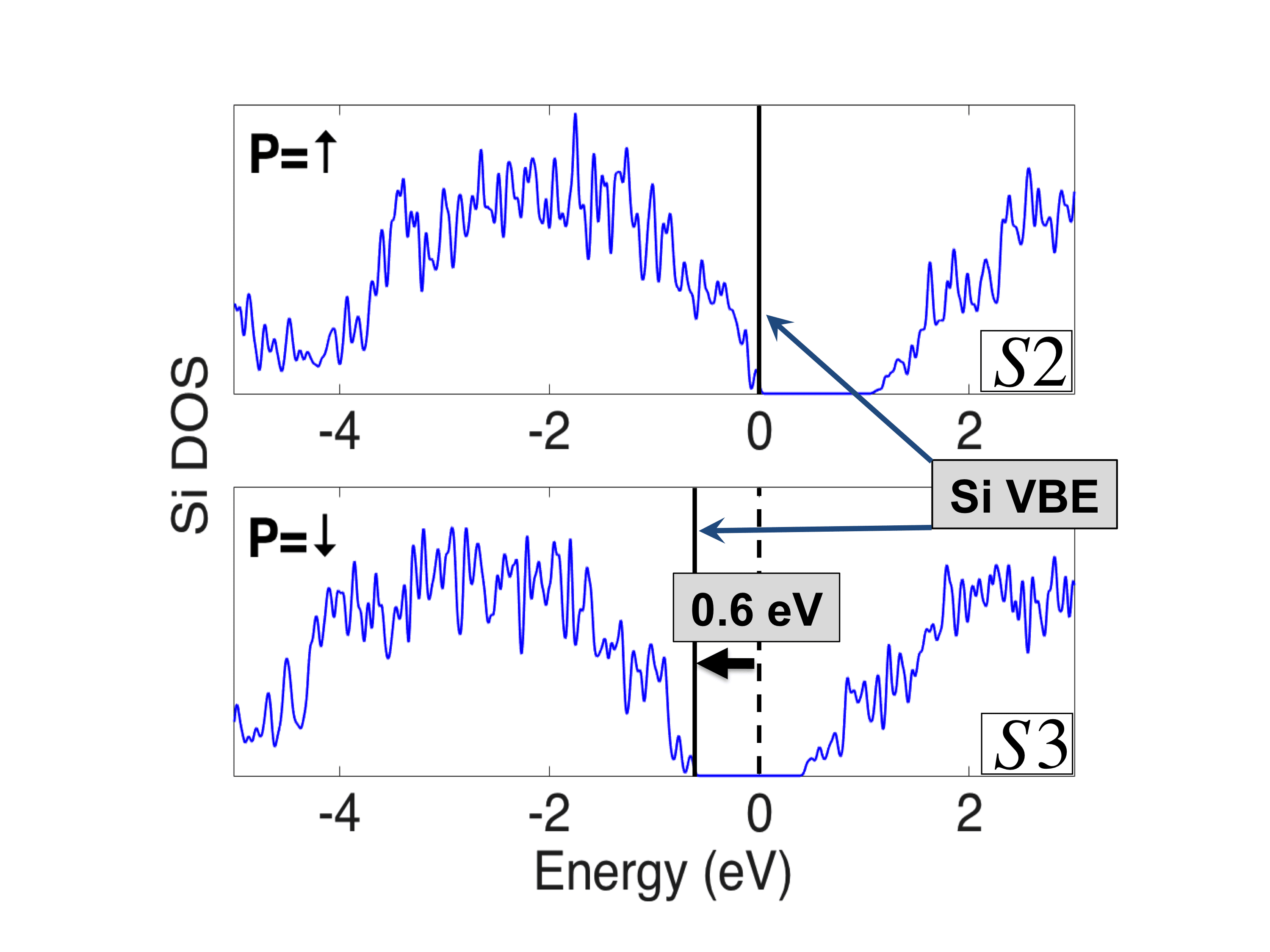
In addition to the prediction that the three lowest energy structures may coexist in monolayer form, in III.3 we will explain why, at temperatures of practical interest, structures and should be the dominant motifs in the monolayer structure. Because of the large difference in polarization together with a low energy barrier between these two structures, we believe that the polarization switching described in Ref. (Dogan et al. 2018) should correspond to switching between and . A first and simple corroboration involves showing that the change in the silicon Fermi level observed in the experiment is comparable with our theoretical prediction. In \FigrefSiZrO2_DOS, we plot the density of states (DOS) of the ZrO2/Si system projected onto an interior layer of the Si substrate for the cases of interface structures and . We set the energy of the Si valence band edge (VBE) of to zero and align the vacuum energy level in to the vacuum energy energy in . We find a eV VBE shift in Si, which is somewhat larger than, but comparable to, the experimental value of eV. We believe that this is due to the fact that the experimental monolayers are not epitaxial but amorphous with multiple structural motifs present, so that application of the electric field is not as effective at polarization switching as is assumed in our clean, epitaxial and ordered theoretical simulations.
III.3 Domain energetics
Up to this point, our theoretical study of the ZrO2 monolayers on the Si(001) surface has shown that (meta)stable configurations with varying polarizations are present. We have also demonstrated that transitions between some of the lowest energy configurations do not require complicated rearrangements of atoms and have low energy barriers. Because of these findings, as well as the fact that the experimental monolayer is amorphous, we expect there to be a multi-domain character to these monolayers at or near room temperature (). However, directly calculating the energy of a multi-domain region of the system for an area larger than a few primitive unit cells is not feasible. In this section, we describe an approximate model Hamiltonian method to compute the energies of arbitrary regions of multiple domains, and use Monte Carlo simulations to find thermodynamic ground states at finite temperatures.
III.3.1 Domain wall energies
In order to investigate the behavior of finite domains, we have developed a lattice model where every in-plane cell is treated as a site in a two dimensional lattice which couples to its neighbors via an interaction energy. Similar models have been proposed for other two dimensional systems (Bune et al. 1998). Such a model is reasonable if the interface (domain wall) between domains of different states is sharp, i.e., the atomic positions a few unit cells away from a domain boundary are indistinguishable from the atomic positions in the center of the domain. To find the degree of locality and the energy costs of the domain walls, we have computed domain wall energies as a function of domain size.
Sample simulation arrangements are shown in \FigrefSiZrO2_latt_cell. In (a) and (b), domain walls along the - and -directions are formed, respectively, between the configurations and . Three unit cells of and each are generated and attached together to build larger simulation cells to model the domain walls: and cells to simulate the domain boundaries along the - and -directions, respectively. In each of the 3 unit wide domains, the center unit is fixed to the atomic configuration of the corresponding uniform system. In \FigrefSiZrO2_latt_cell, for the domain, the atoms in the unit labelled are fixed, and the atoms in the units and are relaxed. The same is true for , but for clarity, fixed units of are displayed on both sides. We then compute the domain wall energy between and by subtracting from the total energy of this supercell and dividing by two. We have checked for a few test cases that increasing the domain width from 3 to 5 cells changes the domain wall energies by small amounts on the order of 1-10 meV while typical domain wall energies are larger than 100 meV (see \TabrefSiZrO2_latt_J). This, together with visualization of the resulting structures, convinces us that the domains are sufficiently local for us to treat the domain walls as being sharp. Note that there are two inequivalent boundaries between and along a given direction. In \FigrefSiZrO2_latt_cell, these boundaries are shown as red and blue dashed lines. Due to the periodicity of simulation cells, it is not possible to compute the energies of these two boundaries independently, so we are forced to assume that their energies are equal.
The final step in determining the domain boundary energies is to survey the configuration space available for a given boundary. For that purpose, for each domain boundary we have generated a number of initial configurations depending on the direction of the boundary:
- •
For a boundary along the -direction such as in \FigrefSiZrO2_latt_cell(a), we have generated five initial configurations as follows. For each domain state (e.g., or ), we have labeled the Zr-O pairs along the -direction and the remaining oxygens and numbered them in an increasing order in the -direction. In the figure, the labelling for states and is shown. Note that for each cell, the sequence starts with a Zr-O pair and ends with an O atom. Hence in some cases the oxygen labelled 4 lies beyond the unit cell to which it belongs, such as in . To build a domain boundary such as the - (shown as a blue dashed line), we first place the atomic groups numbered from to the left hand side of the boundary, and the atomic groups numbered from to the right hand side of the boundary. This constitutes our first initial configuration. The second configuration is obtained by replacing atom from on the left hand side by atom from . The third is obtained by replacing both group and atom from by and from . The fourth choice is to replace atomic group from on the right hand side by group from ; and, lastly, the fifth choice is to replace and from by and from . The opposite operation is performed at the other boundary such as - (shown as a red dashed line). We then take the smallest of the five computed domain energies as the final energy. Note that the relaxed structure shown in the \FigrefSiZrO2_latt_cell(a) for the - domain boundaries is obtained via choice for the - boundary.
- •
For a boundary along the -direction such as in \FigrefSiZrO2_latt_cell(b), we have generated a few initial configurations by slightly and randomly displacing the two oxygen atoms at the boundary along the -direction in order to break the symmetry inherent to these structures.
III.3.2 Construction of a lattice model
Once we have the library of domain boundary energies for every pair of states along the - and -directions described above, we approximate the energy of the system with an arbitrary configuration of domains by a two-dimensional anisotropic lattice Hamiltonian on a square lattice:
| (1) | |||||
where donates the state at a given site , is the energy (per unit cell) of state for a uniform system in that state, and is the energy of interaction (i.e., domain wall energy) between the neighboring states in the axial direction . In our model, only nearest neighbor interactions are included. Because of the anisotropic nature of the film (the - and -directions are fundamentally different due to Si dimerization), the interaction term must distinguish between directions and so that and differ. The domain boundary energies calculated via DFT simulations are employed as nearest neighbor interaction energies in this model. In \FigrefSiZrO2_lattice, we illustrate an arbitrary configuration of such a lattice. As an example, the state in the middle column couples to and via and , respectively, and to and via and , respectively.
For a model with distinct states, our interaction matrices () have the following properties:
- •
The interaction energy between the sites of the same kind is zero by definition, . Hence the number of non-zero entries is .
- •
We have assumed that the domain wall energy between states and remains the same if we swap the states. Therefore the interaction matrices are symmetric , reducing the number of unique non-zero entries to .
- •
In our particular system, every state has a counterpart which is obtained by the reflection . Hence, e.g., the domain wall between and can be obtained from the domain wall between and by applying a single symmetry operation. Therefore many of the entires of are paired up in this way which further reduces the number of unique entries further to .
In \TabrefSiZrO2_latt_J, we list the unique entries of for states ranging over the the six lowest energy states. Note that since for this table, there are entries in the table. Because the unit cell is , the couplings are expected to be smaller than the couplings , which is generally correct. We have computed the domain wall energies for more possible of states including , , and , and the longer list of resulting domain wall energies (see Supplementary Material) are included in our treatment of the lattice model below.
| Domain boundary | (eV) | (eV) |
|---|---|---|
| 0.26 | 1.35 | |
| 0.76 | 1.13 | |
| 0.96 | 0.99 | |
| 0.61 | 4.81 | |
| 0.44 | 1.75 | |
| 0.38 | 1.64 | |
| 0.17 | 0.98 | |
| 0.01 | 0.91 | |
| 0.73 | 0.002 |
We notice that some of the values in \TabrefSiZrO2_latt_J, namely and , are very small, which is expected to be a significant factor in the finite temperature behavior of our model. We demonstrate the domain wall that corresponds to in \FigrefSiZrO2_dom_S3S3b via a top view. Because one of the -Zr-O-Zr-O- chains along the -direction in the unit cell is approximately aligned with the valley between consecutive Si dimers along the -direction, it is approximately unchanged under the transformation. Therefore when and cells are attached in the -direction, continuous and linear -Zr-O-Zr-O- chains are obtained (the top and bottom black horizontal straight lines in \FigrefSiZrO2_dom_S3S3b). The remaining -Zr-O-Zr-O- chain in the unit cells matches imperfectly, but the distortion is small (the winding black horizontal curve in the middle in \FigrefSiZrO2_dom_S3S3b) such that the only atom with a slightly modified environment is one of the oxygen atoms at the domain boundary (encircled with a red dashed ring in the figure). This near-perfect meshing of the -Zr-O-Zr-O- chains after stacking the and structures along the -direction is the cause of the very small energy cost of creating the domain boundary.
The model we have built is a general discrete lattice model that resembles two dimensional Ising models and, more generally, Potts models (Wu 1982). However, due to the lack of any simple pattern in site energies and couplings, it does not belong to any analytically solvable category of models.
III.3.3 Mean-field approach
To understand the thermodynamic behavior of this model at finite temperature, we begin with the standard mean-field approach which is based on the assumption that every site interacts in an averaged manner with its neighboring sites. For a model with states , every site has a probability of being occupied by state . In mean field theory, the energy of such a site including its interactions with its nearest neighbors is given by
| (2) | |||||
The probability is given by the the Boltzmann factor so that
| (3) |
where
| (4) |
is the mean-field partition function.
These equations form a self-consistent system of equations for for a given temperature and the specified energies and couplings , . We present the solutions of this system of equations for temperatures ranging from 0.1 through 3.0 in \FigrefSiZrO2_latt_MF. We find that there is a first-order phase transition at a very high temperature of eV (16,000 K). Below this temperature, one of the two degenerate ground states ( or occupies nearly all the sites (i.e., spontaneous symmetry breaking). Above the transition temperature, the ground states are suppressed and the lattice gets filled by the remaining states with an approximately equal contributions. At very high temperature (not shown in the figure), all states have equal probability, as expected.
It is known that in simpler two dimensional lattice problems, the mean-field approximation predicts correctly the existence of a phase transition but overestimates the critical temperature (Neto et al. 2006). The mean-field approach assumes that each site interacts with all its neighbors in an uncorrelated fashion and neglects the fact that correlation lengths are finite. Moreover, as seen from (), the mean-field equations sum over all neighbors and end up providing “isotropic solutions” (i.e., the and directions become equivalent), which is an serious shortcoming due to the major role anisotropy is expected to, and will, play in our system (see 4). In summary, we expect these mean field theory predictions to be informative but not quantitatively accurate.
III.3.4 Monte Carlo simulations
For a better understanding of our model at temperatures of practical interest, we have employed classical Monte Carlo simulations with a modified version of the Wolff cluster algorithm (Swendsen and Wang 1987; Wolff 1989) that we have developed. For further details of the method, we refer the reader to the Supplementary Material. We have run simulations in a lattice with free boundary conditions (i.e., the lattice is a finite-sized system with zero couplings beyond the edges; comparison to periodic boundary conditions showed no discernible differences for this lattice size at the temperatures examined below). and completely random initial conditions, for 0.016, 0.032, 0.064, 0.128, 0.256 and 0.512 eV. We have used a non-square simulation lattice because of the larger couplings in the -direction compared to the -direction, which lead to longer correlation lengths in the -direction (see below). In \FigrefSiZrO2_latt_MC_ss, a sample configuration of a well-thermalized simulation with () is displayed.
In \FigrefSiZrO2_latt_MC_corr, the autocorrelation functions as a function of simulation step (“time” ) and the horizontal and vertical spatial correlation functions and are plotted for each state for one particular Monte Carlo run. These correlation functions are defined as
| (5) | |||||
| (6) | |||||
| (7) | |||||
where identifies the state at the lattice site () at the simulation time step . We have defined 10 functions (one for each state ) such that if the lattice site () is occupied by state at time and is 0 otherwise. In \FigrefSiZrO2_latt_MC_ss, correlation functions for every type of state (, etc.) are computed separately and overlaid.
We observe that for the run exemplified by \FigrefSiZrO2_latt_MC_ss and analyzed in \FigrefSiZrO2_latt_MC_ss, (1) a 1000 step Monte Carlo simulation leads to decorrelation (i.e., equilibration) of states , , , , and but not for , , and . (2) The simulation cell of size is successful in containing the domains that form at this temperature since the spatial correlations become quite small by the half-way point along each direction of the simulation cell: sites that are sufficiently far from each other are not correlated. We have repeated these simulations 10 times for each temperature and have found that the correlation functions behave similarly when the initial state of the simulation cell is chosen randomly. For temperatures higher than eV, all temporal correlations decay below in the duration of the simulation.
The reason behind the slow temporal decay of the , , and autocorrelations at low temperatures is that large domains of these states form in the lattice, and the Monte Carlo algorithm becomes inefficient in “flipping” these domains to another configuration. To see what other effects are present in these simulations, we monitor two other quantities displayed in \FigrefSiZrO2_latt_MC_other. The first is the probability that any lattice site is occupied by a particular state: we show the ratio of the number of sites occupied by a particular state to the total number of sites in the simulation cell. The second quantity is the average domain size for each state: this is computed for each snapshot at a fixed time by first determining all the domains of that state (including domains with only one site), and then dividing the total number of sites occupied by the state to the number of domains. A large jump in the second quantity during the simulation usually indicates a merger of two domains. The fact that these quantities change quickly at the beginning of the simulation and more slowly toward the end of the simulation in \FigrefSiZrO2_latt_MC_other is indicative that the characteristics seen in \FigrefSiZrO2_latt_MC_ss are representative of large volumes of the configuration space sampled with the Boltzmann distribution at (186 K): namely, while the lattice system has not fully equilibrated, i.e., the temporal correlations have not decayed to very small values, it is not very far from equilibrium either. Hence, these results show that at this low temperature, the lattice system should be dominated by large domains of and followed by smaller domains of and .
We now return to the mean field prediction that at temperatures lower than eV the system should be dominated by either one of the ground states. Clearly, this prediction is not supported by our Monte Carlo simulations. Our Monte Carlo simulations show that for eV, there is no long range order. In 16, we plot the correlation lengths and along the - and -directions, respectively. The correlation lengths are calculated by fitting the spatial correlation functions and to exponentials of the form . We calculate the correlation lengths (averaged over all states) for each run and then average over all runs at a given temperature. As indicated by the temperature dependence of the correlation length , the system gradually becomes more ordered as the temperature is increased up to , and then becomes disordered. Such behavior is associated with a second order phase transition in which correlation lengths diverge upon approaching the critical temperature. If such a critical temperature is present in this system, it lies between () and (). Because the melting temperature of silicon is , it is likely impossible to approach this critical temperature in practice. Hence, it is safe to assume that for the relevant experimental conditions (), the monolayer system is well within the ordered phase.
Finally, we comment on qualitative characteristics of the multi-domain structure of these films based on our lattice model. In \FigrefSiZrO2_latt_MC_Prob, we display the probability for a site to be occupied by each state as a function of temperature, where the probability values are averaged over the last quarter of each run, and then further averaged over 10 runs. The data show that the system is dominated by the second and the third lowest energy configurations (). As discussed above, we believe that this is due to the rather low couplings and when compared to the other couplings in \TabrefSiZrO2_latt_J. Namely, these domain walls are not very costly energetically, so their entropic contribution is significant even at low temperatures and stabilizes these phases even though they are not the lowest energy states.
In \FigrefSiZrO2_latt_MC_Patches we display the average domain size of each state vs temperature, again averaged over 10 runs for each temperature. We find that, on average, the domains of states and are larger than the domains of states and , even though they occupy similar portions of the simulation cell (see 17). This may be because so the and easily form vertical stacks of domains at essentially no energetic cost, as exemplified in \FigrefSiZrO2_latt_MC_ss: some of these stacks are emphasized by black arrows on the left edge of the figure, but there are many more in the interior of the simulation cell.
To sum up, according to our discrete lattice model simulations, for ordered ZrO2 monolayers on the Si(001) surface and the experimentally relevant temperature range of , domains of , , and should be expected to occur with linear extents ranging from a few to a few dozen unit cells. This supports our claim that achieving epitaxy for these films should be challenging. However, given that the local structure is approximated by a mixture of and domains, the observed ferroelectric switching is understandable as being due to a transition between these two states.
IV Conclusion
We have conducted a computational study of ZrO2 monolayers on Si(001) using DFT. These monolayers have recently been grown with as an abrupt oxide/semiconductor interface but with an amorphous structure and are measured to be ferroelectric (Dogan et al. 2018). In our computations, we have found a multiplicity of (meta)stable structures with a large variation in ionic polarization but small differences in energy, atomic structure and chemistry. This suggests that achieving epitaxy in the experiment should be challenging. In order to understand the finite-temperature behavior of these ultrathin films, we have developed a two dimensional discrete lattice model of the domains in these thin films using DFT-derived parameters. We have employed mean-field and Monte Carlo calculations to study this lattice model and concluded that two distinct and oppositely polarized structures, namely , and their counterparts and , dominate the films at the temperatures of interest. The ferroelectric switching observed in the experiment is explained by the film locally adopting one of these two structures and locally switching between them. We have found that for monocrystalline epitaxial films, this switching leads to a VBE shift in silicon of , which is moderately greater than the experimental value of , in agreement with the idea of partial (local) polarization switching.
V Acknowledgements
This work was supported primarily by the grant NSF MRSEC DMR-1119826. We thank the Yale Center for Research Computing for guidance and use of the research computing infrastructure, with special thanks to Stephen Weston and Andrew Sherman. Additional computational support was provided by NSF XSEDE resources via Grant TG-MCA08X007.
References
- Dogan et al. (2018) M. Dogan, S. Fernandez-Peña, L. Kornblum, Y. Jia, D. P. Kumah, J. W. Reiner, Z. Krivokapic, A. M. Kolpak, S. Ismail-Beigi, C. H. Ahn, et al., Nano Letters 18, 241 (2018), ISSN 1530-6984, URL http://dx.doi.org/10.1021/acs.nanolett.7b03988.
- Hwang et al. (2012) H. Y. Hwang, Y. Iwasa, M. Kawasaki, B. Keimer, N. Nagaosa, and Y. Tokura, Nature Materials 11, 103 (2012), ISSN 1476-1122, URL http://www.nature.com/nmat/journal/v11/n2/abs/nmat3223.html.
- Mannhart and Schlom (2010) J. Mannhart and D. G. Schlom, Science 327, 1607 (2010), ISSN 0036-8075, 1095-9203, URL http://science.sciencemag.org/content/327/5973/1607.
- Reiner et al. (2009) J. W. Reiner, F. J. Walker, and C. H. Ahn, Science 323, 1018 (2009), ISSN 0036-8075, 1095-9203, URL http://www.sciencemag.org/content/323/5917/1018.
- Reiner et al. (2010) J. W. Reiner, A. M. Kolpak, Y. Segal, K. F. Garrity, S. Ismail-Beigi, C. H. Ahn, and F. J. Walker, Advanced Materials 22, 2919 (2010), ISSN 1521-4095, URL http://onlinelibrary.wiley.com/doi/10.1002/adma.200904306/abstract.
- Dogan and Ismail-Beigi (2017) M. Dogan and S. Ismail-Beigi, Physical Review B 96, 075301 (2017), URL https://link.aps.org/doi/10.1103/PhysRevB.96.075301.
- McKee et al. (2001) R. A. McKee, F. J. Walker, and M. F. Chisholm, Science 293, 468 (2001), ISSN 0036-8075, 1095-9203, URL http://www.sciencemag.org/content/293/5529/468.
- Garrity et al. (2012) K. F. Garrity, A. M. Kolpak, and S. Ismail-Beigi, Journal of Materials Science 47, 7417 (2012), ISSN 0022-2461, 1573-4803, URL http://link.springer.com/article/10.1007/s10853-012-6425-z.
- Batra et al. (1973) I. P. Batra, P. Wurfel, and B. D. Silverman, Physical Review B 8, 3257 (1973), URL http://link.aps.org/doi/10.1103/PhysRevB.8.3257.
- Dubourdieu et al. (2013) C. Dubourdieu, J. Bruley, T. M. Arruda, A. Posadas, J. Jordan-Sweet, M. M. Frank, E. Cartier, D. J. Frank, S. V. Kalinin, A. A. Demkov, et al., Nature Nanotechnology 8, 748 (2013), ISSN 1748-3387, URL http://www.nature.com/nnano/journal/v8/n10/full/nnano.2013.192.html.
- Robertson (2006) J. Robertson, Reports on Progress in Physics 69, 327 (2006), ISSN 0034-4885, URL http://iopscience.iop.org/0034-4885/69/2/R02.
- McDaniel et al. (2014) M. D. McDaniel, T. Q. Ngo, A. Posadas, C. Hu, S. Lu, D. J. Smith, E. T. Yu, A. A. Demkov, and J. G. Ekerdt, Advanced Materials Interfaces 1, n/a (2014), ISSN 2196-7350, URL http://onlinelibrary.wiley.com/doi/10.1002/admi.201400081/abstract.
- McKee et al. (1998) R. A. McKee, F. J. Walker, and M. F. Chisholm, Physical Review Letters 81, 3014 (1998), URL http://link.aps.org/doi/10.1103/PhysRevLett.81.3014.
- Kumah et al. (2016) D. P. Kumah, M. Dogan, J. H. Ngai, D. Qiu, Z. Zhang, D. Su, E. D. Specht, S. Ismail-Beigi, C. H. Ahn, and F. J. Walker, Physical Review Letters 116, 106101 (2016), URL http://link.aps.org/doi/10.1103/PhysRevLett.116.106101.
- Perdew et al. (1996) J. P. Perdew, K. Burke, and M. Ernzerhof, Physical Review Letters 77, 3865 (1996), URL http://link.aps.org/doi/10.1103/PhysRevLett.77.3865.
- Vanderbilt (1990) D. Vanderbilt, Physical Review B 41, 7892 (1990), URL http://link.aps.org/doi/10.1103/PhysRevB.41.7892.
- Giannozzi et al. (2009) P. Giannozzi, S. Baroni, N. Bonini, M. Calandra, R. Car, C. Cavazzoni, Davide Ceresoli, G. L. Chiarotti, M. Cococcioni, I. Dabo, et al., Journal of Physics: Condensed Matter 21, 395502 (2009), ISSN 0953-8984, URL http://stacks.iop.org/0953-8984/21/i=39/a=395502.
- Marzari et al. (1999) N. Marzari, D. Vanderbilt, A. De Vita, and M. C. Payne, Physical Review Letters 82, 3296 (1999), URL http://link.aps.org/doi/10.1103/PhysRevLett.82.3296.
- Bengtsson (1999) L. Bengtsson, Physical Review B 59, 12301 (1999), URL http://link.aps.org/doi/10.1103/PhysRevB.59.12301.
- Henkelman et al. (2000) G. Henkelman, B. P. Uberuaga, and H. Jónsson, The Journal of Chemical Physics 113, 9901 (2000), ISSN 0021-9606, 1089-7690, URL http://scitation.aip.org/content/aip/journal/jcp/113/22/10.1063/1.1329672.
- Ramstad et al. (1995) A. Ramstad, G. Brocks, and P. J. Kelly, Physical Review B 51, 14504 (1995), URL http://link.aps.org/doi/10.1103/PhysRevB.51.14504.
- Paz et al. (2001) Ó. Paz, A. J. R. da Silva, J. José Sáenz, and E. Artacho, Surface Science 482–485, Part 1, 458 (2001), ISSN 0039-6028, URL http://www.sciencedirect.com/science/article/pii/S0039602800010220.
- Bune et al. (1998) A. V. Bune, V. M. Fridkin, S. Ducharme, L. M. Blinov, S. P. Palto, A. V. Sorokin, S. G. Yudin, and A. Zlatkin, Nature 391, 874 (1998), ISSN 0028-0836, URL http://www.nature.com/nature/journal/v391/n6670/full/391874a0.html.
- Wu (1982) F. Y. Wu, Reviews of Modern Physics 54, 235 (1982), URL http://link.aps.org/doi/10.1103/RevModPhys.54.235.
- Neto et al. (2006) M. A. Neto, R. A. dos Anjos, and J. R. de Sousa, Physical Review B 73, 214439 (2006), URL http://link.aps.org/doi/10.1103/PhysRevB.73.214439.
- Swendsen and Wang (1987) R. H. Swendsen and J.-S. Wang, Physical Review Letters 58, 86 (1987), URL http://link.aps.org/doi/10.1103/PhysRevLett.58.86.
- Wolff (1989) U. Wolff, Physical Review Letters 62, 361 (1989), URL http://link.aps.org/doi/10.1103/PhysRevLett.62.361.