Single Photon Detection by Cavity-Assisted All-Optical Gain
Abstract
We consider the free carrier dispersion effect in a semiconductor nanocavity in the limit of discrete photoexcited electron-hole pairs. This analysis reveals the possibility of ultrafast, incoherent transduction and gain from a single photon signal to a strong coherent probe field. Homodyne detection of the displaced probe field enables a new method for room temperature, photon-number-resolving single photon detection. In particular, we estimate that a single photon absorbed within a silicon nanocavity can, within tens of picoseconds, be detected with efficiency and a dark count rate on the order of kHz assuming a mode volume for a 4.5 m probe wavelength and a loaded quality factor on the order of .
I Introduction
An outstanding goal in optoelectronics is the development of a room temperature single photon detector that simultaneously achieves high count rate, low timing jitter, low dark count rate, and photon-number-resolution. Room temperature single photon detectors have been developed in a range of materials and platforms Hadfield 2009; Zhang et al. 2015, but their performance remains limited by the need to concurrently design optical absorption and electrical readout mechanisms Ma et al. 2015. Jitter performance in avalanche photodiodes (APDs), for example, is limited by the inhomogeneous travel time of carriers, while thermal noise and electronic defects within the amplification region contribute to high false detection rates, a phenomenon which is particularly significant in non-Si APDs Hadfield 2009; Eisaman et al. 2011. Despite decades of development of passive and active reset mechanisms, reset times are also still long — typically tens to hundreds of nanoseconds Hadfield 2009; Zhang et al. 2015. Alternatively, superconducting single photon detectors enable high detection efficiency, low dark count rates, and few-ps jitter, but require cryogenic cooling and have limited count rates due to their long dead times Natarajan et al. 2012; Dauler et al. 2014; Korzh et al..
These examples of state-of-the-art photodetectors illustrate the limitations inherent to amplification in the electronic domain: high thermal noise as well as slow carrier and amplifier response times. Here, we propose a new class of room temperature semiconductor photodetectors that addresses these limitations by realizing single photon amplification in the optical domain. This readout technique retains the benefits of an optical channel: negligible thermal noise, large bandwidth, and low-loss transmission.
Fig. 1(a) illustrates the concept. The absorption of a signal photon in a semiconductor optical cavity excites a free electron-hole charge carrier pair (Fig. 1(b)), which nearly instantaneously shifts the solid-state medium’s refractive index — and in turn the cavity’s resonant frequency — through the free carrier dispersion effect (Fig. 1(c)). The resulting change in resonant frequency imparts a phase shift on a transmitted probe field that can be measured using heterodyne or homodyne detection with common high-speed p-i-n photodetectors Piels and Bowers 2016; DeRose et al. 2011; Chen et al. 2017. Because a single photogenerated electron-hole pair can scatter multiple probe photons, this process produces all-optical gain. The change in cavity transmission induced by a single signal photon can therefore be converted into a strong probe signal at the homodyne receiver. Here, we analyze this all-optical amplification process and determine the experimental requirements for efficient single photon detection.
II Free carrier dispersion due to a single electron-hole pair
Suppose that a single photon is absorbed at the center of a cavity as shown in Fig. 1(a). According to first order perturbation theory, the photo-excited free electron-hole pair causes a fractional resonance shift Joannopoulos et al. 2008
| (1) |
due to the permittivity shift within the electric field profile . In accordance with the Drude model, we assume that the fractional index change is directly proportional to the free carrier density. Therefore, if the free carrier pair is confined within a small “hot spot” volume (over which can be assumed to be constant) near the cavity’s peak energy, Eqn. 1 simplifies to
| (2) |
where we have introduced the standard optical mode volume Note1 and the “effective scattering volume” as the constant of proportionality between and carrier density (). This result is identical to the frequency shift generated from a uniform carrier density throughout the mode volume. The resulting fractional resonance shift with respect to the linewidth for a cavity with quality factor is
| (3) |
In other words, for any given , a high ratio is desired. Silicon photonic crystal (PhC) cavities are therefore an ideal candidate, as recent fabrication advances have enabled cavities with intrinsic s of with Sekoguchi et al. 2014; Asano et al. 2017 and alternatively s of with mode volumes reaching Hu et al. 2018.
In silicon, can be approximated in two ways. The Drude model in the high frequency limit yields 11 1 See attached supplemental material for further discussion., where is the electron charge, is the vacuum permittivity, is the probe frequency, and and are the effective masses of the electron and hole, respectively. Given the effective masses , of free carriers in undoped silicon at room temperature Jacoboni et al. 1977; Soref and Bennett 1987, we find if a m probe wavelength is used to eliminate two photon absorption. Alternatively, can be approximated from the empirical formula Soref and Bennett 1987; Nedeljkovic et al. 2011
| (4) |
where () is the free electron (hole) density, and , , , and , are the wavelength () dependent coefficients tabulated in Nedeljkovic et al. 2011. Eqn. 4 follows from absorption measurements in silicon for wavelengths between 1.3 and 14 m. Linearizing this model about , we find , a factor of 3 different from the previous estimate.
Both values indicate that a linewidth-order frequency shift requires a quality factor on the order of for a probe optical mode volume , or alternatively for . As discussed below, optimization of the cavity architecture enables high signal-to-noise ratio (SNR) homodyne detection of the output probe signal with a fractional linewidth shift, even further reducing the necessary . The approach is therefore applicable to both standard diffraction-limited PhC cavities, as well as state-of-the-art subwavelength-confined nanocavities Hu et al. 2018. Our subsequent analysis assumes an index change provided by Eqn. 4 due to the experimentally observed nonlinear scaling with respect to carrier density.
Any index change induced by free carrier dispersion is accompanied by a corresponding loss: free carrier absorption (FCA). The associated absorptive quality factor Xu et al. 2009 for an additional FCA loss of , is therefore of interest. For a single electron-hole pair confined to within the suggested modes volume in silicon, Nedeljkovic et al. 2011; Note1. Since we consider cavities with intrinsic quality factors on the order of , we ignore this effect.

Other nonlinearities, such as the optical Kerr effect, could be similarly enhanced within these PhC cavities, as the intra-cavity intensity scales with Soljacić and Joannopoulos 2004; Nozaki et al. 2010. However, free carrier nonlinearities based on real transitions, while incoherent, are significantly stronger than those resulting from virtual transitions. The effect is also broadband in semiconductors, as any absorbed signal photon produces a free electron-hole pair. Free carrier nonlinearities have previously enabled all-optical switching at GHz speeds with sub-femtojoule ( photons) switching energies Nozaki et al. 2010. While switching requires , we show that photodetection can be achieved with , which reduces the required input energy to the single photon level for recently developed high- PhC cavities.
III Detector Optimization
We analyze the two photodetection architectures shown in Fig. 2(a,b) using a temporal coupled mode theory approach Haus 1984; Fan et al. 2003; Suh et al. 2004. The simplest configuration (Fig. 2(a)) consists of: 1) a single signal cavity, similar to that of Fig. 1, to amplify the phase shift generated by the photoexcited charge carriers; and 2) a homodyne receiver to measure the phase shift of the probe field leaving the cavity. The temporal evolution of the cavity field amplitude , assuming input and output probe coupling rates and respectively, is governed by the characteristic equation Haus 1984
| (5) |
where is the input power, is the intra-cavity energy, is the cavity resonant frequency (aligned to the probe frequency ), and is the loaded cavity amplitude decay time. Following the resonance shift generated by the absorption of a signal photon, the shot noise-limited SNR obtained from a homodyne measurement of the displaced output field during a detection window of duration can be approximated analytically using first order perturbation theory as Note1
| (6) |
which is directly proportional to the number of probe photons output in response to the resonance shift (SNR=) Loudon 2000. Eqn. 6 illustrates the symmetric dependence of the detection performance upon the input and output probe coupling rates to the signal cavity, and , respectively. In general, faster coupling rates limit the detector sensitivity but enable the displaced probe signal to be rapidly extracted, while the opposite is true for slow coupling rates. Optimizing the SNR with respect to and yields the optimum loaded quality factor, , shown in Fig. 2(c) (assuming an intrinsic quality factor ), which produces the SNR shown in Fig. 2(d) for a 2.3 m probe wavelength.
The results demonstrate that a SNR1 is achievable within 50 ps for a sub-W probe power due to the all-optical gain afforded by the detection cavity. Notably, the optimal loaded quality factors () for these short (sub-50 ps) integration times are much less than , indicating that can be further reduced without substantial degradation of the detection SNR. Similar results are obtained for Note1; however, the input power required for high-SNR detection within a given time increases.
The coupled-cavity architecture shown in Fig. 2(b) can be used for “cavity dumping” to reduce the required probe power. The evolution of the two cavities, assumed to be resonant with the input probe frequency , is described by the coupled differential equations
| (7) | ||||
| (8) |
where () is the tunnel (signal) cavity amplitude that decays at rate () for the coupling times shown in Fig. 2(b). The waves and couple the tunnel and signal cavities, which are separated by a distance corresponding to an effective phase . If Note1 for any integer , the wave output from destructively interferes with at , corresponding to the high- regime of the two cavity system. The phase shift produced through the absorption of a signal photon within disturbs this interference condition, causing rapid evacuation of the stored cavity field. This effect, analogous to “cavity dumping” for pulse generation in laser resonators Pshenichnikov et al. 1994, has been previously implemented to achieve ultrafast tuning of photonic crystal cavities Tanaka et al. 2007 and integrated ring resonators Xu et al. 2007.
Given these considerations, we numerically optimized the coupling rates of Eqns. 7 and 8 to maximize the SNR in Eqn. 6, yielding the loaded quality factors shown in Fig. 2(c) and associated SNR in Fig. 2(d). These simulations indicate that the power reduction is proportional to , which can be understood as the amplification of stored energy in the high- regime.
Furthermore, in the perturbative limit, the functional form of the SNR provided in Eqn. 6 shows that is proportional to the square of the resonance shift, and is thereby a function of the number of absorbed signal photons . Fig. 2(f) demonstrates this scaling for a 10 W input probe power. For small , the trend is well fitted by considering the biexponential behavior of the refractive index shift in Eqn. 4. The growth of with respect to is large enough to enable photon number resolution of the signal field. This is illustrated by the well-separated Poissonian distributions of in the inset of Fig. 2(f) for .
Overall, these optimized results demonstrate that a single silicon nanocavity can enable ultrafast, high-efficiency, and even number resolving single photon detection. Cavity dumping in a two-cavity system can reduce the probe field power by over an order of magnitude. This improvement also opens the possibility of monitoring a large array of detectors with a significantly reduced input probe power. Moreover, jitter contributions for the all-optical photodetector are limited to fluctuations in the signal photon absorption time, probabalistic variation in the output probe field, and the jitter of the homodyne photodetectors. As the first two are negligible for high-efficiency detection Note1, the achievable jitter is limited by that of the photodetectors used to measure the classical probe field.
IV Dark Count Contributions
The aforementioned analysis considered the probe laser shot noise as the sole source of noise. In reality, dark counts — erroneous detection events which occur in absence of a signal beam — must be carefully considered. Any fast (on the order of the detector integration time ) change in the cavity refractive index above contributes to the dark count rate, as slow changes can be high-pass filtered. We consider three principal factors: thermal excitation of free carriers, temperature fluctuations of the semiconductor substrate, and multiphoton absorption. While surface defect states may contribute to the dark count rate, we omit this contribution due to the record-low surface recombination velocity of silicon Yablonovitch et al. 1986.
Given an intrinsic carrier concentration of in pure silicon at 300 K, the mean population within the proposed mode volume at a 2.3 m probe wavelength is . The resulting probability of a non-zero thermal carrier population within the optical mode is approximately equal to this mean occupancy Note1 and corresponds to a 10 kHz dark count rate for a GHz detector gating frequency. Cooling to 200 K reduces this dark count rate to a negligible sub-Hz rate Note1. The dark count rate from temperature variation of the substrate is likewise negligible if the temperature is stabilized to K (where K-1 is silicon’s thermo-optic coefficient) such that thermo-optic refractive index changes are smaller than those induced by a single absorbed photon. Fundamental statistical temperature fluctuations within the cavity — which typically limit PhC cavity sensitivity Saurav and Le Thomas 2017 — are an order of magnitude smaller than this value Note1, and the stability requirement can therefore be readily achieved with modern PID temperature controllers Lee et al. 2016.
While both thermally induced free carriers and direct index variations due to the thermo-optic effect in silicon can be mitigated with proper environmental control Note1, multiphoton absorption (MPA) events — given the indistinguishably between probe- and signal-induced free carriers within the cavity — produce a dark count rate that can only be lowered by minimizing the intensity of the probe laser within the signal cavity, and thus inherently reducing the sensitivity of the detector. The overall dark count rate from MPA is
| (9) |
where is the MPA coefficient for -photon absorption (PA) and is the probe intensity at a position . Re-expressing this definition in terms of the peak cavity intensity , we find Note1
| (10) |
where the multiphoton absorption mode volume is defined as
| (11) |
For the deep subwavelength () “tip”-based cavities of interest to this study Hu and Weiss 2016; Choi et al. 2017; Hu et al. 2018, a defect in the cavity geometry yields a localized, high intensity region within the broader diffraction-limited mode size Boroditsky et al. 1998. We studied the mode profile of the silicon tip cavity in Choi et al. 2017 to determine the scaling of in this case, yielding the mode volumes summarized in Table 1 Note1. A significant volume reduction is achieved for , revealing an advantage of the tip-based cavity for low noise, all-optical photodetection — suppression of higher order noise processes.
| Probe Wav. [m] | MPA Coefficient (Process) Bristow et al. 2007; Pearl et al. 2008; Gai et al. 2013 | |
|---|---|---|
| 2.3 | 2.5 cm3/GW2 (3PA) | 7.82 |
| 3.4 | 2.5 cm5/GW3 (4PA) | 2.00 |
| 4.5 | 1.4 cm7/GW4 (5PA) | 6.14 |
Given the ability to accurately estimate the dark count rate in Eqn. 10 using the parameters in Table 1, we re-optimize the cavity coupling rates with respect to the figure-of-merit
| (12) |
such that the maximum output is achieved for a given intra-cavity intensity or dark count rate. Since the FOM is independent of input power, both the single and coupled cavity architectures achieve the same optimum value of Note1
| (13) |
for the loaded quality factors shown in Fig. 2(c). Eqn. 10 can then be re-parameterized in terms of this FOM and the shot noise limited detection efficiency , yielding Note1
| (14) |
Assuming a linear scaling of with carrier density as in the Drude model, the dark count rate scales as , revealing the performance enhancement that can be achieved by minimizing the optical mode volume. Longer wavelengths also reduce multi-photon absorption.
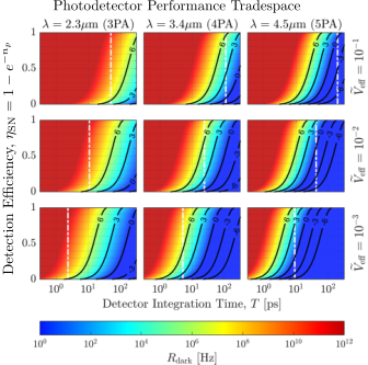
The optimized detection tradespaces — dark count rate as a function of the desired detection efficiency and integration time — for the cavity parameters in Table 1 are plotted in Figure 3 for various effective volumes . The results confirm the aforementioned suppression of dark counts at small mode volumes and long wavelengths. For example, the baseline parameters of the previous section (2.3m and ) result in a dark count rate on the order of 100 kHz given a 50% detection efficiency and 20 ps integration time; however, this rate can be reduced to below 0.01 Hz at 4.5 m.
While optical switching experiments Tanabe et al. 2008; Nozaki et al. 2010; Turner-Foster et al. 2010 seek to minimize the ps-scale diffusion times of photogenerated carriers to maximize the achievable switching frequency, Fig. 3 demonstrates the advantage of reduced dark counts with an extended detection time. The maximum integration time is limited by carrier diffusion for small mode volume PhC cavities Tanabe et al. 2008; Aldaya et al. 2017. To extend this time (estimated by the vertical dashed lines in Fig. 3 assuming an ambipolar diffusion constant cm2/s in silicon Nozaki et al. 2010), charge confinement techniques, such as the incorporation of a double heterostructure Alferov 2001, may be necessary. Even in the absence of charge confinement, the performance tradespace illustrates that an appropriate combination of probe wavelength and cavity volume can be selected to achieve the desired detection characteristics. Most importantly, these optimized metrics demonstrate the ability to realize efficient single photon detection within tens of picoseconds using experimentally achievable parameters.
The resulting overall detection efficiency is limited by the absorption efficiency of the incident signal photon within the mode volume of the probe cavity. For standard suspended silicon photonic crystal cavities with at m, numerical simulations yield a peak efficiency for focused visible light, and could be achieved by incorporating anti-reflection and reflection coatings on the top and bottom surfaces of the cavity, respectively Note1. However, absorption within the subwavelength-confined mode volumes () characteristic of tip defect cavities is limited to Note1. Future work will therefore consider techniques for localized signal light absorption within ultrasmall mode volume nanocavities. Possible approaches include the design of a doubly-resonant cavity for the probe and signal fields Rivoire et al. 2011; Hueting and Cryan 2014 or the incorporation of a selective absorber, such as a buried heterostructure Matsuo et al. 2010, at the center of the cavity.
V Conclusion
In summary, we have analyzed a new concept for single photon detection based on all-optical gain in a nanocavity system. The proposed amplification mechanism can be of use in a range of all-optical signal processing applications, and in particular opens the possibility of room-temperature single photon detection. A single cavity suffices to implement the scheme, and interference with a second cavity can reduce the required input power by orders of magnitude. Multiphoton absorption is a dominant noise process, but the resulting dark count rate can be minimized through a combination of a long-wavelength probe field, a subwavelength confining nanocavity, squeezed light Note1, or the use of a wide bandgap probe cavity material. The proposed dielectric cavity-based system for room temperature, low power, ultrafast single photon detection would prove useful in a wide range of photonic technologies.
The authors thank H. Choi and C. Peng for providing the mode profiles evaluated in this study. C.P. was supported by the Hertz Foundation Elizabeth and Stephen Fantone Family Fellowship and the MIT Jacobs Presidential Fellowship. M.H. was supported by Villum Fonden. R.H. is supported by an appointment to the IC Postdoctoral Research Fellowship Program at MIT, administered by ORISE through U.S. DOE/ODNI. This work was supported in by by the AFOSR MURI for Optimal Measurements for Scalable Quantum Technologies (FA9550-14-1-0052) and by the AFOSR program FA9550-16-1-0391, supervised by Gernot Pomrenke.
References
- Hadfield (2009) R. R. H. R. Hadfield, Nature Photonics 3, 696 (2009).
- Zhang et al. (2015) J. Zhang, M. A. Itzler, H. Zbinden, and J.-W. Pan, Light: Science & Applications 4 (2015), 10.1038/lsa.2015.59.
- Ma et al. (2015) J. Ma, M. Zhou, Z. Yu, X. Jiang, Y. Huo, K. Zang, J. Zhang, J. S. Harris, G. Jin, Q. Zhang, and J.-W. Pan, Optica 2, 974 (2015).
- Eisaman et al. (2011) M. D. Eisaman, J. Fan, A. Migdall, S. V. Polyakov, and . J. Fan, Citation: Review of Scientific Instruments 82 (2011), 10.1063/1.3610677.
- Natarajan et al. (2012) C. M. Natarajan, M. G. Tanner, and R. H. Hadfield, Supercond. Sci. Technol 25, 63001 (2012).
- Dauler et al. (2014) E. A. Dauler, M. E. Grein, A. J. Kerman, F. Marsili, S. Miki, S. W. Nam, M. D. Shaw, H. Terai, V. B. Verma, and T. Yamashita, Optical Engineering 53, 081907 (2014).
- (7) B. A. Korzh, Q.-y. Zhao, S. Frasca, J. P. Allmaras, T. M. Autry, E. A. Bersin, M. Colangelo, G. M. Crouch, A. E. Dane, T. Gerrits, F. Marsili, G. Moody, E. Ramirez, J. D. Rezac, M. J. Stevens, E. E. Wollman, D. Zhu, P. D. Hale, K. L. Silverman, R. P. Mirin, S. W. Nam, M. D. Shaw, and K. K. Berggren, arXiv Optics arXiv:1804.06839v1, arXiv:arXiv:1804.06839 .
- Piels and Bowers (2016) M. Piels and J. E. Bowers, Photodetectors (2016) pp. 3–20.
- DeRose et al. (2011) C. T. DeRose, D. C. Trotter, W. a. Zortman, A. L. Starbuck, M. Fisher, M. R. Watts, and P. S. Davids, Optics Express 19, 24897 (2011).
- Chen et al. (2017) H. Chen, M. Galili, P. Verheyen, P. De Heyn, G. Lepage, J. De Coster, S. Balakrishnan, P. Absil, L. Oxenlowe, J. Van Campenhout, and G. Roelkens, Journal of Lightwave Technology 35, 722 (2017).
- Joannopoulos et al. (2008) J. D. Joannopoulos, S. G. Johnson, J. N. Winn, and R. D. Meade, Princeton (Princeton University Press, 2008) p. 286, arXiv:arXiv:1011.1669v3 .
- (12) See attached supplemental material for further discussion.
- Sekoguchi et al. (2014) H. Sekoguchi, Y. Takahashi, T. Asano, and S. Noda, Optics Express 22, 916 (2014).
- Asano et al. (2017) T. Asano, Y. Ochi, Y. Takahashi, K. Kishimoto, and S. Noda, Optics Express 25, 1769 (2017).
- Hu et al. (2018) S. Hu, M. Khater, R. Salas-Montiel, E. Kratschmer, S. Engelmann, W. M. Green, and S. M. Weiss, Science Advances 4 (2018), 10.1126/sciadv.aat2355, arXiv:1707.04672 .
- Jacoboni et al. (1977) C. Jacoboni, C. Canali, G. Ottaviani, and A. Alberigi Quaranta, Solid-State Electronics 20, 77 (1977).
- Soref and Bennett (1987) R. A. Soref and B. R. Bennett, IEEE Journal of Quantum Electronics 23, 123 (1987).
- Nedeljkovic et al. (2011) M. Nedeljkovic, R. Soref, and G. Z. Mashanovich, IEEE Photonics Journal 3, 1171 (2011).
- Xu et al. (2009) T. Xu, M. S. Wheeler, H. E. Ruda, M. Mojahedi, and J. S. Aitchison, Optics Express 17, 8343 (2009).
- Soljacić and Joannopoulos (2004) M. Soljacić and J. D. Joannopoulos, Nature materials 3, 211 (2004).
- Nozaki et al. (2010) K. Nozaki, T. Tanabe, A. Shinya, S. Matsuo, T. Sato, H. Taniyama, and M. Notomi, Nature Photonics 4, 477 (2010).
- Haus (1984) H. Haus, Waves and Fields in Optoelectronics (Prentice Hall, 1984).
- Fan et al. (2003) S. Fan, W. Suh, and J. D. Joannopoulos, Journal of the Optical Society of America A 20, 569 (2003), arXiv:9605103 [cs] .
- Suh et al. (2004) W. Suh, Z. Wang, and S. Fan, IEEE Journal of Quantum Electronics 40, 1511 (2004).
- Loudon (2000) R. Loudon, The Quantum Theory of Light (Oxford University Press, New York, 2000).
- Pshenichnikov et al. (1994) M. S. Pshenichnikov, W. P. De Boeij, and D. A. Wiersma, Optics Letters 19 (1994).
- Tanaka et al. (2007) Y. Tanaka, J. Upham, T. Nagashima, T. Sugiya, T. Asano, and S. Noda, Nature materials 6, 862 (2007).
- Xu et al. (2007) Q. Xu, P. Dong, and M. Lipson, Nature Physics 3, 406 (2007).
- Yablonovitch et al. (1986) E. Yablonovitch, D. L. Allara, C. C. Chang, T. Gmitter, and T. B. Bright, Physical Review Letters 57, 249 (1986).
- Saurav and Le Thomas (2017) K. Saurav and N. Le Thomas, Optica 4, 757 (2017).
- Lee et al. (2016) J. S. Lee, L. Carroll, C. Scarcella, N. Pavarelli, S. Menezo, S. Bernabe, E. Temporiti, and P. O’Brien, IEEE Journal of Selected Topics in Quantum Electronics 22, 409 (2016).
- Hu and Weiss (2016) S. Hu and S. M. Weiss, ACS Photonics 3, 1647 (2016).
- Choi et al. (2017) H. Choi, M. Heuck, and D. Englund, Physical Review Letters 118 (2017), 10.1103/PhysRevLett.118.223605.
- Boroditsky et al. (1998) M. Boroditsky, R. Coccioli, E. Yablonovitch, Y. Rahmat-Samii, and K. Kim, IEE Proceedings - Optoelectronics 145, 391 (1998).
- Bristow et al. (2007) A. D. Bristow, N. Rotenberg, and H. M. van Driel, Applied Physics Letters 90, 191104 (2007).
- Pearl et al. (2008) S. Pearl, N. Rotenberg, and H. M. van Driel, Applied Physics Letters 93, 131102 (2008).
- Gai et al. (2013) X. Gai, Y. Yu, B. Kuyken, P. Ma, S. J. Madden, J. Van Campenhout, P. Verheyen, G. Roelkens, R. Baets, and B. Luther-Davies, Laser and Photonics Reviews 7, 1054 (2013).
- Tanabe et al. (2008) T. Tanabe, H. Taniyama, and M. Notomi, Journal of Lightwave Technology 26, 1396 (2008).
- Turner-Foster et al. (2010) A. C. Turner-Foster, M. A. Foster, J. S. Levy, C. B. Poitras, R. Salem, A. L. Gaeta, and M. Lipson, Optics Express 18, 3582 (2010).
- Aldaya et al. (2017) I. Aldaya, A. Gil-Molina, J. L. Pita, L. H. Gabrielli, H. L. Fragnito, and P. Dainese, Optica (2017), 10.1364/OPTICA.4.001219, arXiv:1707.07646 .
- Alferov (2001) Z. I. Alferov, Reviews of Modern Physics 73, 767 (2001).
- Rivoire et al. (2011) K. Rivoire, S. Buckley, and J. Vučković, Optics Express 19, 22198 (2011).
- Hueting and Cryan (2014) N. A. Hueting and M. J. Cryan, Journal of the Optical Society of America B 31, 3008 (2014).
- Matsuo et al. (2010) S. Matsuo, A. Shinya, T. Kakitsuka, K. Nozaki, T. Segawa, T. Sato, Y. Kawaguchi, and M. Notomi, Nature Photonics 4, 648 (2010).