Layout and Assembly Technique of the GEM Chambers for the Upgrade of the CMS First Muon Endcap Station
Abstract
Triple-GEM detector technology was recently selected by CMS for a part of the upgrade of its forward muon detector system as GEM detectors provide a stable operation in the high radiation environment expected during the future High-Luminosity phase of the Large Hadron Collider (HL-LHC). In a first step, GEM chambers (detectors) will be installed in the innermost muon endcap station in the pseudo-rapidity region, mainly to control level-1 muon trigger rates after the second LHC Long Shutdown. These new chambers will add redundancy to the muon system in the -region where the background rates are high, and the bending of the muon trajectories due to the CMS magnetic field is small. A novel construction technique for such chambers has been developed in such a way where foils are mounted onto a single stack and then uniformly stretched mechanically, avoiding the use of spacers and glue inside the active gas volume. We describe the layout, the stretching mechanism and the overall assembly technique of such GEM chambers.
Key Words– CMS, GEM, High Luminosity LHC
1 Introduction
The current schedule of the CERN Large Hadron Collider (LHC) includes several long shutdown periods to allow for upgrades of the accelerator complex as well as the experiments. The ultimate upgrade of the LHC to enable operation at a proton-proton center-of-mass energy of 14 TeV with an instantaneous luminosity gradually increasing up to 5-7 1034 cm-2s-1 is referred to as the High Luminosity LHC (HL-LHC). After the two-year long second Long Shutdown (LS2) starting in 2019, the instantaneous luminosity will exceed 2 1034 cm-2 s-1, while the third Long Shutdown (LS3) scheduled for 2024-2026 will bring the LHC luminosity to its ultimate level of about 5 to 7 times its design value. The HL-LHC (or Phase-2) period starting after LS3 and currently foreseen up to 2035, is expected to yield a total integrated luminosity of about 3000 fb-1.

During the HL-LHC period, the Compact Muon Solenoid (CMS) experiment [1] will continue its present physics program and therefore needs to maintain its sensitivity for electroweak scale physics and for TeV scale searches. As such, the CMS Collaboration is planning several detector upgrades in order to maintain or improve its high level of performance, in particular also of its muon system [2]. Presently, as can be seen in Figure 1, only Cathode Strip Chambers (CSC) are installed in the forward region of the CMS muon system. To increase redundancy and enhance the muon trigger and reconstruction capabilities in that particular region, several additional muon stations will be added [4]. A first step will be the installation during LS2 of an additional set of muon chambers denoted as GE11 in the first muon endcap disks. The GE11 chambers11 1 In ”GE11”, the ”G” stands for GEM and the ”E” for Endcap; the first ”1” corresponds to the first muon station and the second ”1” to the first, innermost ring of the station will contain Gas Electron Multiplier (GEM) technology [5] which given its known excellent rate capability and radiation hardness is well-suited for this forward detector region.
2 GE11 motivation
During the HL-LHC operation, the increase of the beam energy and the collision rate compared to the current situation will definitely affect the radiation environment of the detector. First of all, the increase of the background rate in the forward region of the CMS muon endcaps will provoke a rise of the CMS level-1 muon trigger rate and a degradation of the muon selection due to trigger bandwidth limitations. Therefore, the challenge associated with the forward region of the muon system for the HL-LHC is to maintain an efficient and reliable trigger in the region. High muon trigger rates in the forward region of the detector are driven by the fast drop in the magnetic field towards high , which results in a decreased bending of muon trajectories as they traverse the CMS muon system. As the measurement of muon pT by the CMS level-1 muon trigger is effectively based on the observed bending of muon trajectories, any degradation in the muon pT resolution will lead to higher trigger rates due to the increased probability of low-pT particles being reconstructed as high-pT muons.
In addition, the high radiation background may accelerate the aging of the current muon system and could cause performance losses and dead regions. The expected background in the CMS endcaps for an instantaneous luminosity of 5 1034 cm-2s-1 has been computed using the CMS adaptation of the FLUKA simulation package and was found to be dominated by neutrons and secondary particles arising from neutron interactions with matter. Neutrons with energies ranging from thermal values to a few GeV originate from interactions of hadrons produced in primary pp collisions with the beam pipe material and structures in the very forward region. Neutron interactions within the detector material lead to secondary particles, mostly high-energy photons and electrons, that can produce detectable amounts of ionization in gaseous detectors. The sensitivity of muon detectors to background particles with different energies has been computed using the GEANT4 framework [4]. The background spectrum has been convoluted with the sensitivity to provide the expected hit rate in the detectors. The maximum hit rate in the first muon station is expected to be around 5 kHzcm2 at the HL-LHC, with an estimated integrated charge of about 100 mC/cm2 for 20 years of HL-LHC operation [4].
This implies that the upgraded forward muon system must be sufficiently resistant to radiation and have a high rate capability. Furthermore, it must offer adequate pattern recognition capability to allow for efficient reconstruction of muon tracks while minimizing the number of mis-identified tracks. Part of the solution chosen by the CMS Collaboration is the introduction of additional, GEM technology based gaseous detectors in the forward endcaps to complement the current CSC system. The new GE11 station in the first endcap disks together with the current muon system will enable the CMS trigger to better discriminate high- muons from low- muons [4]. In particular, the GE11 station will extend the total path length of the muon system in that -region and will provide additional hits that will help to refine the stub reconstruction and improve the momentum resolution. With the new station installed, muon direction will be measured using hit positions in the adjacent GEM GE11 and CSC ME11 chambers in the same -region. The good position resolution of both detectors and the increased lever arm formed by the two detectors will allow for an improved measurement of muon direction and bending angle in the CMS magnetic field. The rate of misidentified muons as well as the L1 trigger rate will also be reduced. The reduction of trigger rate will allow maintaining a low momentum threshold, therefore increasing the acceptance and efficiency of reconstruction of soft muons.
3 The GE11 station
GEM detectors exploit the electron amplification that occurs within a gas medium inside narrow holes that perforate a thin polyimide foil in a triangular pattern. The polymide foil is clad on both sides with a thin conductive copper layer. With a voltage up to about 400 volts applied across the two copper-clad surfaces of a foil a strong electric field (60-100 kVcm) is produced inside the GEM holes. The primary electrons produced due to ionization of the gas by a charged particle passing through the chamber drift towards the holes and once they start experiencing the very intense electric field inside the holes, they acquire enough kinetic energy to produce secondary ionization in the gas. This process eventually leads to the formation of an electron avalanche. An arrangement of three cascaded GEM foils, commonly known as a "triple-GEM detector", allows a high charge amplification factor up to several 105 for modest applied high voltage, which limits the probability of electrical breakdown. The amplified charge induces a measurable signal on a readout electrode that can be segmented to provide positional information.
The GE11 detectors are trapezoidally shaped and consist of a gas volume containing a stack of three large-area GEM foils, i.e. a triple-GEM detector, embedded between a drift electrode and a readout board, with an induction/transfer-1/transfer-2/induction gap configuration of 3121 mm. The first transfer gap has been set in order to minimize the charge released after the first GEM. The induction gap has been set to achieve induction field up to 5 kVcm without too much increase in the potential across the entire structure. The baseline gas mixture for operating the CMS triple-GEMs is Ar/CO2 in 70:30 proportion.

In the GE1/1 stations, a pair of triple-GEM detectors is combined to form a "super-chamber" that provides two measurement planes to maximize detection efficiency. Each super-chamber covers a 10.15∘ sector so that 36 super-chambers are required to form a ring that gives full azimuthal coverage as can be seen in Figure 2. To instrument both endcap disks, i.e. two GE1/1 stations, a total of 72 super-chambers or 144 basic chamber units are required. The super-chambers will alternate in phi between long and short versions as dictated by the mechanical envelope of the existing endcap disk, i.e. each endcap disk will hold 18 long and 18 short super-chambers.
Over the past years, the performance of several generations of GE11 chamber prototypes was studied in a series of beam tests at CERN and Fermilab [6, 7]. With 98.0 chamber efficiency, a GE11 super-chamber will have an efficiency above 99.9 when the logical OR of the signals from the two basic units is taken.
4 Chamber design
The structure of a basic GE1/1 unit is shown in Figure 3. A chamber consists of a drift board, three identical GEM foils stacked together within frames, a readout board and an external gas frame. The drift and readout boards and the external frame define the gas volume with the gas tightness ensured by an O-ring placed inside a groove in the external frame. This construction allows the detectors to be thin, which is important given the limited space available within the existing CMS detector. Because of mechanical constraints due to support structures in the GE1/1 station, two versions of detectors were designed in order to maximize detection coverage. Long chambers have a radial length of 128.5 cm, while short chambers have a radial length of 113.5 cm. The main technical specifications of the GE1/1 detectors for both the Long and Short versions are listed in Table 1.

| GE1 detector | ||
|---|---|---|
| Specification | Short | Long |
| Shape | Trapezoidal | Trapezoidal |
| Chamber Length | 113.5 cm | 128.5 cm |
| Chamber Width | (28.5-48.4) cm | (28.6-51.2) cm |
| Chamber thickness | 1.42 cm | 1.42 cm |
| Active readout area | 3787 cm 2 (app.) | 4550 cm2 (app.) |
| Active chamber volume | 2.6 liters | 3 liters |
| Geometric acceptance in | 1.61-2.18 | 1.55-2.18 |
The design of the drift board, the external and internal frames, the GEM foils, the readout board and the gas distribution system are described in the following subsections.
4.1 The drift board
The GE1/1 drift board is a trapezoidal-shaped printed circuit board holding the drift electrode. The actual board and the magnified view of its wider side is shown in Figure 4. The board has an active area coated with a copper layer, i.e. the drift electrode, that is contained in the active gas volume. GEM foils are electrically connected to the HV power supply using spring-loaded pins. As shown in Figure 5, these HV pins are mounted on the drift board, at positions corresponding to the HV pads located on the GEM foils. Four pins are foreseen for each foil, i.e. a bottom and top side contact plus two spare pins. Pins for a given GEM foil, i.e. at a given height in the stack, have an identical height height. The drift board has number of holes around the periphery to accommodate mechanical stainless steel pieces called pull-outs, that are used to stretch the foils as will be explained in Section 5.3.


Other on-board elements are outside the gas volume. There are pads for a 10 M protection resistor that is used to limit the current from the HV power supply. There are pads for a 100 k resistor and a 330 pF capacitor used to decouple the signal from the HV when during the post-assembly chamber quality control procedure a detector signal is extracted from the bottom of the third GEM foil. Finally, there are HV traces as shown in Figure 4.
4.2 The external frame
The GE1/1 external frame is shown in Figure 6. It is made up of halogen-free glass-epoxy material, machined from a single piece. The frame is used to close the active gas volume between the drift and readout boards. It has a trapezoidal shape and has numerous wide notches to accommodate the stainless steel pull-outs. It is coated with Nuvovern polyurethane varnish before assembly to seal in particulates. Narrow grooves are machined on both sides in order to accommodate a Viton O-ring.


4.3 The internal frame

The design of the internal frames is shown in Figure 7. There are four layers of internal frames made from halogen-free glass epoxy with thickness of 3 mm, 1 mm, 2 mm, and 1 mm. Each frame is composed of 10 individual pieces per layer. The pieces are coated with Nuvovern polyurethane varnish before assembly which ensures that no glass epoxy particulates get detached from the frames during the chamber assembly as any dust falling onto the GEM foils could produce electrical shorts in the holes. Small threaded M2 brass inserts are fixed within the 3 mm frame to avoid loosening of macroscopic and microscopic glass epoxy particulates from the frames when screws pass through the frame. The frame layers are stacked and define the 3121 mm spacings between the drift board, the triple-GEM structure and the readout board.


4.4 The GEM foils
The GE11 detector uses three identical trapezoidal-shaped GEM foils as shown in Figure 9. The foils are produced at the CERN PCB workshop using a single-mask production technique [8]. The GEM foil surfaces oriented towards the readout board are a single continuous conductor whereas the GEM foil surfaces oriented towards the drift board are segmented into sectors. The sectors run across the trapezoid in the same direction as the parallel ends. The sector width (in the radial direction) is largest at the short end of the trapezoid and smallest at the wide end so that the area of each sector is approximately the same, about 100 cm2. This segmentation limits the charge and energy in case of a discharge. In an extreme case, if a discharge large enough to generate a short were to occur in a particular HV segment, it would render unusable only that particular HV segment and not the entire foil. Therefore, each segment has a separate connection to the HV supply via a trace around the edge of the GEM foil to a common connection point at the wide end. Each trace is connected through a 10 M surface-mounted protection resistor that limits the current from the HV supply, decouples the capacitance from other HV sectors, and quenches a discharge. The voltage for the other side of the foil is connected at two points located at the wide end of the foil, where the two points provide redundancy.


4.5 The readout board

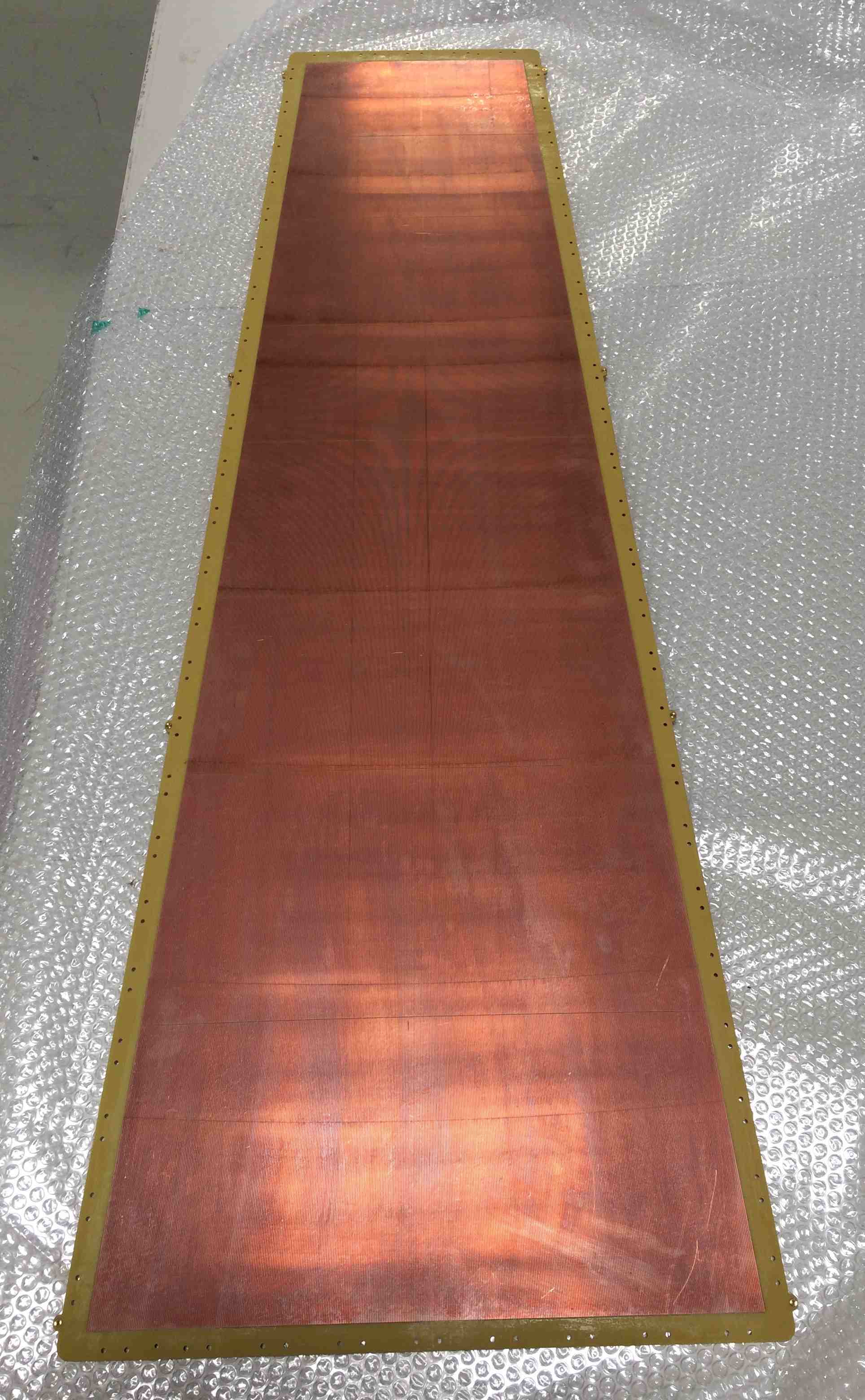
The readout board is a trapezoidal-shaped printed circuit board with mechanical design as shown in Figure 10. The inner side of the board features 3072 trapezoidal readout strips oriented radially along the longer sides of the chamber. The active area covered by the strips subtends an azimuthal angle of 10.15∘ which allows for an overlap of 0.15∘ (equivalent to 5.67 strips) between the active areas of adjacent chambers. All the readout strips are connected through metalized vias to the outer side of the board where traces are routed from the vias to readout pads in partitions of 8 3 partitions in (, ). Each -partition has 384 strips comprised of three 128-strip sectors in . The strip pitch varies between 0.6 mm at the shorter end of the chamber and 1.2 mm at the wider end. The readout board has two holes at diagonally opposed corners, in which gas plugs are mounted that serve as inlet and outlet explained in Section 4.7.


4.6 On-chamber HV distribution to the GEM foils and drift electrode
As described in Section 4.1, the GEM foils are powered through high voltage pins soldered onto the drift board within the gas volume, the design of which is shown in Figure 12, while an actual photograph is shown in Figure 14. These pins get pushed against their corresponding connection pads on the GEM foils which are at different heights as shown in Figures 12 and 13. The HV pins are connected with pads outside the gas volume. These pads are designed in order to allow to power the GEM chambers either using multi-channel or single channel power supply. In the later case, the pads will be used to fix a special resistive divider network which allows a correct voltage distribution to the GEM foils. The circuit diagram for the 3121 mm chamber gap configuration is shown in Figure 14.


4.7 Gas distribution within the chamber
Gas connections to each GE1/1 chamber are made with a single inlet and a single outlet located on diagonally opposite corners of the readout board. The design of a gas plug fixed on the readout board is shown in Figure 15. The gas mixture flows diagonally through the chamber and the presence of the GEM stack in the gas volume (i.e., between the Readout, external frame, and Drift boards) directs the gas flow towards the other corners and makes the flow laminar. The gas distribution inside the GEM stack (i.e. between GEM foils) is made possible by diffusion through the gaps between the inner frames and through the GEM holes.

5 Assembly technique
Any kind of contamination can make a GE11 detector fail as particles going inside the 10 micron diameters holes of the GEM foils can cause electrical shorts. Therefore, the assembly of such detectors takes place in a clean room environment of ISO class 6. The use of tools with lubricated shafts, soldering equipment that requires heating of volatile fluxes, motors and vacuum pipes with out-gassing oils, hair and fingernail cosmetics are sources which can possibly contaminate the detector and are forbidden in the assembly area.
For the construction of the very first GE1/1 prototype, the GEM foils were initially thermally stretched during 24 hours at 37∘ in a special oven [9]. Fiberglass spacer frames were then glued onto the foils in order to fix and keep them separated at the correct distance in the triple-GEM configuration. This procedure was however prone to possible glue contamination, very time-consuming and labour-intensive and therefore not well suited for mass production. This glueing assembly procedure was eventually abandoned after the construction of the first two generations of GE11 chambers. Alternative methods were tested to stretch GEM foils including stretching due to infrared heating lamps [10]. However, a major development in the GE11 chamber assembly procedure was introduced in 2011 with a new technique [6, 11] in which the GEM foils are mechanically stretched and the chamber is constructed without the use of any glue. The technique was initially tested on small 3030 cm2 prototypes [12] and later used to construct actual GE1/1 chambers [14, 15]. Since no glue is needed during the assembly this technique reduces the chamber assembly time from several days to a few hours only, and also allows for a chamber to be reopened in case of problems.
The important steps performed during the assembly of a GE11 chamber are discussed in the forthcoming sections. The procedure starts with the preparation of the drift board, followed by the assembly of the GEM stack. Next, the GEM foils are mechanically stretched using the above mentioned new technique after which the chamber is closed by the readout board.
5.1 Drift board preparation
The drift board is prepared outside the clean room in order to avoid the contamination of the clean room due to the soldering of different components which must be mounted on the board. Twelve pins are mounted on the drift board for making HV connections to the corresponding GEM foils. The three sets of pins have different heights to properly reach the three GEM foils in the stack. Pull-outs are bolted onto the perimeter of the drift PCB with two stainless steel M 3 6/ 8 screws that are sealed with polyamide washers against the drift board to prevent gas leakage. As described already in Section 4.1, a surface mounted (SMD) 10 M Resistor, a 330 pF Capacitor and a 100 k resistor are also soldered to the drift board.
5.2 GEM stack assembly
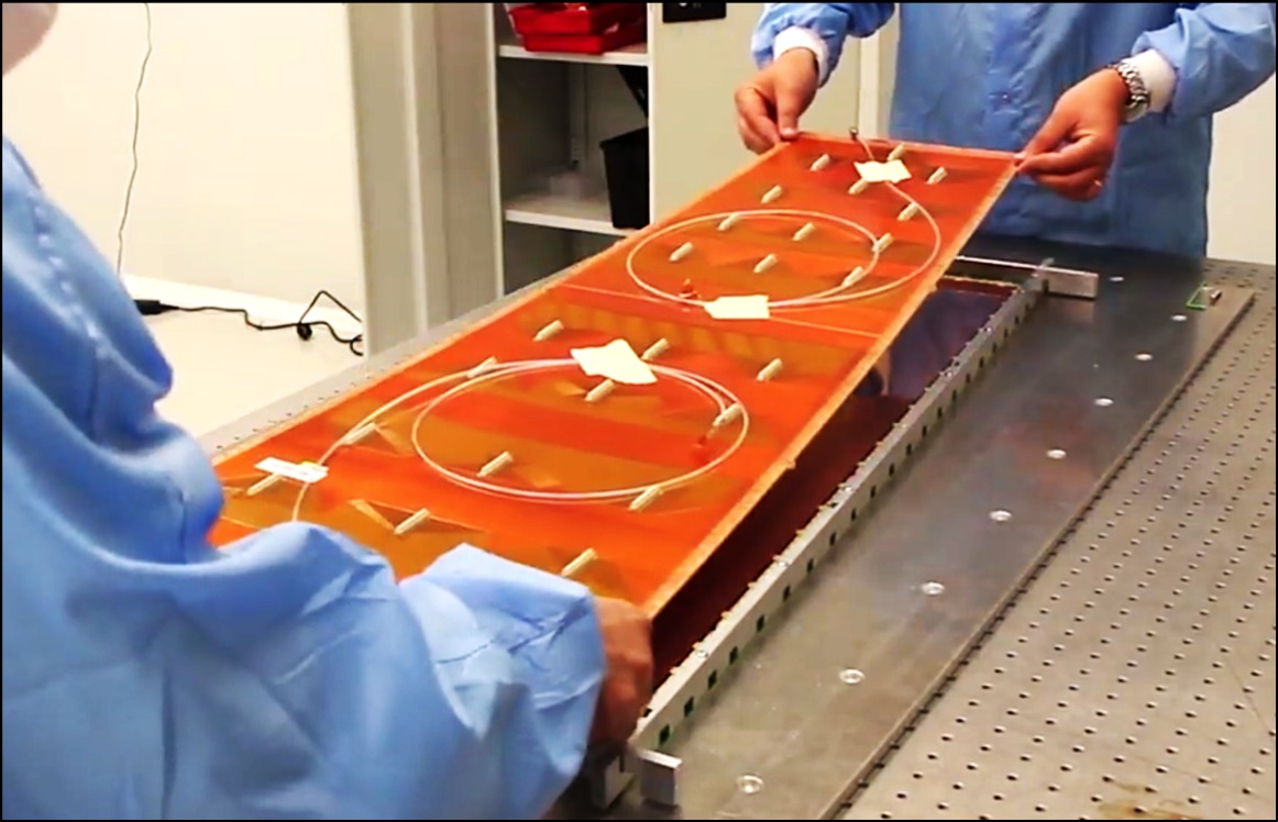
The most critical part in the chamber construction is the preparation of the GEM foil stack, which is realized with the help of a Plexiglas base plate that includes alignment pins at desired positions to keep the entire structure aligned during the assembly procedure. These alignment pins are fixed into the Plexiglas sheet following the trapezoidal geometry demanded by the mechanical layout of the detector. In the stack, the internal frame pieces fabricated in FR4 material are alternated with the GEM foils to define the different gaps. The 10 pieces of the 3 mm frames are inserted first over the alignment pins before placing the first GEM foil as shown in Figure 16.

Before placing a GEM foil on the stack, it is first cleaned using an antistatic adhesive roller, which removes dust particles at the micron level by its strong sticking capacity as shown in Figure 17 (left). This is followed by a leakage current measurement in which a potential difference of 550 V is applied across the foil using an insulation tester as shown in Figure 17 (right). The applied potential produces a very high electric field, typically of the order of 70-100 kV/cm, within the GEM holes and may lead to initial sparks due to the burning of any dust particles within the GEM holes. As such, this test may effectively help to clean the foils from leftover impurities. In an environment with 30 of relative humidity (RH) or less, the maximum allowed value of the leakage current when a potential difference of 550V is applied across the foils is 35 nA. However, above 30 of RH, the leakage current can drastically rise above that level. During this test, electrostatic charge is accumulated inside the GEM holes making them more likely to catch any remaining dust particles. Moreover, during the mounting of the stack, the GEM foils are not yet perfectly stretched, and if two adjacent foils in the stack come in contact, the whole energy accumulated on the foils can be released in a single point which may lead a damaged GEM foil. For this reason, at the end of the leakage current test, the GEM foils must be fully discharged by shorting the top and bottom electrodes.


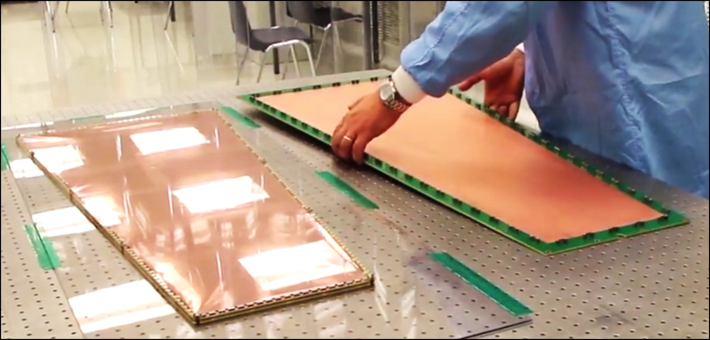
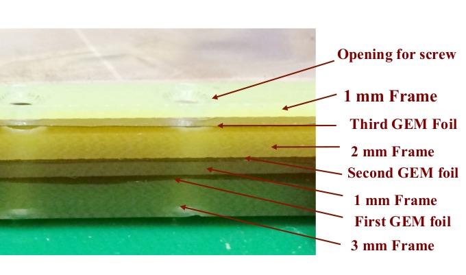
As was shown already in Figure 9, the edges of the GEM foils have a pattern of holes, which are used to attach the foils to internal frames. The stack of three GEM foils is formed by sandwiching foils at their edges between the four layers of internal frames described in Section 4.3. A detailed view of these frames is shown in Figure 18. The stack is held together by numerous small M 2 6 non-magnetic stainless steel screws, spaced about every centimeter along the frame and penetrating all the frame layers and foils. These screws are tightened against small threaded M2 brass inserts. After the second GEM foil is placed on the stack followed by the 2 mm frame, stainless steel nuts are embedded into the frames (at specifically designed "" shaped grooves) every few centimeters around the periphery of the stack, with the axes of their threaded holes oriented parallel to the plane of the inner frame. These nuts together with the pull-outs mounted on the drift board and the corresponding screws are used in the stretching mechanism as will be explained in Section 5.3. The GEM stack consisting of three foils with the 3121 mm frames is finished by removing the dead area surrounding the active area of the foils as shown in Figure 19.
5.3 GEM foil stretching mechanism
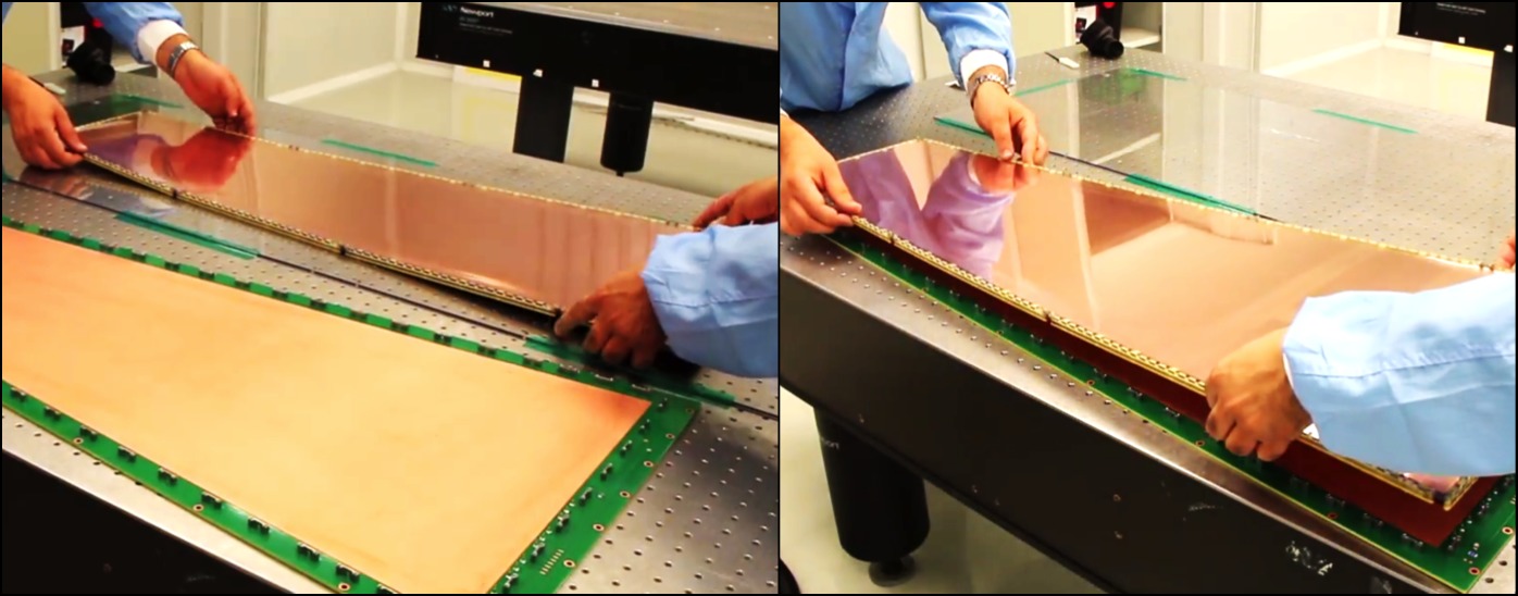

After the preparation of the three-layered GEM stack as described in Section 5.2, this stack is then placed over the drift board as shown in Figure 20 (top). The drift board is fixed against a special assembly jig made of aluminium bars which are tightened with the help of fixation bolts as shown in Figure 20 (bottom). The jig is used to keep the drift board flat by preventing deformations during the stretching of the GEM stack or during the fixation of the readout board against it when closing the chamber at the end of the assembly procedure.

Next, the entire GEM stack is mechanically stretched, i.e. all three foils at once, following the technique that is conceptually visualized in Figure 21. The nuts inserted after the second GEM foil is put on the stack as explained in Section 5.2 recieves M 2.58/8 stainless steel screws that are inserted laterally into the pull-outs located within the gas volume on the drift board as shown in Figure 22 (top). The stack is then uniformly stretched against the pull-outs by amanually applying a controlled torque of about 8-10 cNm on the lateral screws, pulling the inner frame outwards towards the pull-outs as shown in Figure 22 (bottom). In order to lower the risk of forming "waves" in the GEM foils during the stretching of the stack, a specific order is followed in the tightening of the screws. Pairs of corresponding screws on opposite sides of the chamber are tightened simultaneously by two people.


Tolerances inherent in the stretching mechanism of the GEM foils and their relative positioning can have an impact on the uniformity of the gas gain and the detector timing response. It is therefore crucial to ensure uniform stretching during assembly in order to achieve a uniform response across the detector surface. This uniform stretching is ensured by setting specifications on the torques applied to the pull-out screws during assembly. To determine and validate the optimal mechanical tension applied to the GEM foils, a procedure involving Fiber Bragg Grating (FBG) sensors was used [13].
5.4 Closing the chamber
After the foil stretching, a connectivity test between the gaps and across the foils is performed by measuring the impedance using a Mega Ohm Insulation tester. This is done by applying a potential difference of 550 V across the GEM foils and in between different gaps through the HV traces outside of the gas volume on the drift board. An impedance of more than 100 G and 15 G is expected between the gaps and across each GEM foil, respectively, for RH of 30 or less. The impedance may have lower values at higher values of humidity.

At the end of the assembly procedure, the external frame is placed around the tensioned GEM stack. It defines the limits of the gas volume as shown in Figure 23. The anode readout board is placed on top of this outer frame and is attached to the stainless steel pull-outs with A2 stainless steel M3 6 8 screws which are sealed with polyamide washers against the readout board as shown in Figure 24. This sandwiches the outer frame tightly between the drift and readout boards and provides a solid gas barrier. The final detector is shown in Figure 24.

6 Summary and outlook
As part of its High Luminosity LHC upgrade project, the CMS Collaboration recently approved the use of GEM technology to extend its muon system in the forward region. In a first step, 144 new triple-GEM chambers (GE1/1) will be added to the first muon endcap stations during the upcoming second LHC Long Shutdown. After several years of RD that started in 2009, the design of these CMS GE11 chambers has been finalized. The chambers are constructed using a novel mechanical stretching system requiring no gluing during assembly and no spacers inside the active area of the detector. This assembly technique reduces the chamber construction time from several days to a few hours only. Before reaching the final design, several full-size prototype chambers were produced using this stretching technique and were successfully operated in test beams [6, 7, 14].
The final integration of the GE1/1 chambers into the CMS muon system is now being prepared. Following the design and assembly technique described here, ten chambers have been assembled, tested and installed inside the CMS experiment during the 2017 Extended Year End Technical Stop (EYETS) [3]. These chambers are providing the first operational experience with GEM detectors inside CMS. The installation and integration time required later on for the full GE1/1 station can now be optimized. The production and quality control of chambers for the full GE1/1 system is on schedule for installation in 2019.
Acknowledgements
We gratefully acknowledge the support from FRS-FNRS (Belgium), FWO-Flanders (Belgium), BSF-MES (Bulgaria), BMBF (Germany), DAE (India), DST (India), INFN (Italy), NRF (Korea), LAS (Lithuania), QNRF (Qatar), DOE (USA) and the RD51 collaboration.
References
- [1]
CMS Collaboration, JINST, 3 (2008) S08004.
http://iopscience.iop.org/article/10.1088/1748-0221/3/08/S08004 - [2]
CMS Collaboration, JINST, 13 (2008) P06015.
http://iopscience.iop.org/article/10.1088/1748-0221/13/06/P06015 - [3] D. Abbaneo et al., "Operational experience with the GEM detector assembly lines for the CMS forward muon upgrade", IEEE Transactions on Nuclear Science (2018) submitted.
- [4]
CMS Collaboration, CMS TDR, CERN-LHCC-2015-012 (2015).
https://cds.cern.ch/record/2021453?ln=en - [5]
F. Sauli et al., NIMA. A386 (1997) 531.
https://inspirehep.net/record/457577?ln=fr - [6]
D. Abbaneo et al., IEEE Nucl. Sci. Symp. Conf. (2012) N14-137.
http://ieeexplore.ieee.org/document/6551293/ - [7]
D. Abbaneo et al., IEEE Nucl. Sci. Symp. Conf., (2011) 1806-1810.
http://ieeexplore.ieee.org/document/6154688/ - [8]
S. D. Pinto et al., JINST 4 (2009) 12009.
http://iopscience.iop.org/1748-0221/4/12/P12009 - [9]
D. Abbaneo, et al., IEEE Nucl. Sci. Symp. Conf., (2011) 1909.
http://ieeexplore.ieee.org/stamp/stamp.jsp?arnumber=5874107 - [10] M. Staib et al., CERN-LHCC-2015-012 (2011), RD51-Note-004.
- [11]
D. Abbaneo et al., JINST 8 (2013) C12031.
http://iopscience.iop.org/1748-0221/8/12/C12031 - [12]
M. Tytgat et al., IEEE Nucl. Sci. Symp. Conf. (2011) 1019.
http://ieeexplore.ieee.org/document/6154312/ - [13]
D. Abbaneo et al., 4th Int. Conf. on MPGD 174 (2018) 03002.
https://doi.org/10.1051/epjconf/201817403002 - [14]
D. Abbaneo et al., IEEE Nucl. Sci. Symp. Conf. (2014) 1-8.
http://ieeexplore.ieee.org/document/7431249/ - [15]
D. Abbaneo et al., NIMA 718 (2013) 383-386.
http://dx.doi.org/10.1016/j.nima.2012.10.058