Time-dependent density functional theory for interaction
of ultrashort light pulse with thin materials
Abstract
We present a comprehensive theoretical description for an irradiation of an ultrashort light pulse normally on thin materials based on first-principles time-dependent density functional theory. As the most elaborate scheme, we develop a microscopic description solving Maxwell equations for light electromagnetic fields and the time-dependent Kohn-Sham equation for electron dynamics simultaneously in the time domain using a common spatial grid. We call it the microscopic Maxwell-TDDFT scheme. We test this scheme for silicon thin films of various thickness, from a few atomic layers to a few tens of nm. We show that the microscopic Maxwell-TDDFT scheme provides a satisfactory description incorporating electronic structure of thin films in the first-principles level, multiple reflections of the electromagnetic fields at the surfaces, and nonlinear light-matter interaction when the incident light pulse is strong. However, the calculation becomes expensive as the thickness increases. We then consider two limiting cases of extremely thin and sufficiently thick films and develop approximate schemes. For the extremely thin case including two-dimensional atomic-layered materials, a two-dimensional macroscopic electromagnetism is developed: a two-dimensional susceptibility is introduced for a weak field, while time evolution equation is derived for an intense field. For sufficiently thick films, the microscopic Maxwell-TDDFT scheme is expected to coincide with a description utilizing ordinary macroscopic electromagnetism. We numerically confirm it comparing the calculated results: For a weak field, a comparison is made with a description using the bulk dielectric susceptibility. For a strong field, a comparison is made with a multiscale Maxwell-TDDFT scheme which the authors’ group developed previously.
I Introduction
Electronic and optical properties of thin materials have been extensively explored. Thin materials of thickness comparable to or less than the wavelength of light are important for optical coating and devicesKats and Capasso 2016. Quantum wells have been attracting interests for their unique optical properties due to the electron confinement in two-dimensional (2D) regionKelly and Nicholas 1985. In the last decade, there have been an explosion of researches on 2D sheet materials such as graphene and transition metal dichalcogenideNovoselov et al. 2005; Nair et al. 2008; Britnell et al. 2013; Wang et al. 2012; Won and Shigekawa 2010. In recent optical sciences, optical responses of thin materials using intense and ultrashort laser pulses are carried out quite often to explore electron dynamics in the time domainKrausz and Ivanov 2009; Bonaccorso et al. 2010; Calegari et al. 2016; Nicoletti and Cavalleri 2016.
Under these experimental progresses, theories for the interaction of light with thin materials have been actively studied. Because electronic structures of thin materials are quite different from those of bulk materials, quantum mechanical description for the electronic structure is indispensable. For the light propagation in thin materials, theories utilizing response functions, or equivalently, transfer matrix have been developed for weak pulsesSaleh and Teich 2007; Pendry 1996; Katsidis and Siapkas 2002; Zhan et al. 2013; Li and Heinz 2018; Gupta et al. 2018. However, for the interaction of intense and ultrashort light pulse, problems of electronic structure and light propagation are no more separated. Thus, it becomes important to develop a comprehensive theory that treats both electronic structures of thin materials and light propagation dynamics in thin materials simultaneously.
This paper aims to report our progresses to develop a theoretical and computational scheme that describes the interaction of ultrashort light pulse and thin materials, from one atomic layer to a few tens of nm thickness. In our theoretical description, we rely upon the time-dependent density functional theory (TDDFT) for electron dynamicsRunge and Gross 1984. TDDFT is an extension of the ordinary density functional theory that successfully describes ground states of electronic systems so that it describes electronic excitations and dynamics induced by an external field. The basic equation that we solve is the time-dependent Kohn-Sham (TDKS) equation.
Combined with a linear response theory, TDDFT has been quite successful to describe electronic excitations and optical responses of molecules and solidsCasida 2009; Laurent and Jacquemin 2013; Paier et al. 2008; Yabana and Bertsch 1996; Bertsch et al. 2000; Yabana et al. 2006. Solving the TDKS equation in real time, it can describe nonlinear and ultrafast electron dynamics induced by intense and ultrashort laser pulsesPetersilka and Gross 1999; Calvayrac et al. 2000; Tong and Chu 2001; Nobusada and Yabana 2004; Castro et al. 2004; Otobe et al. 2008; Shinohara et al. 2010; Miyamoto et al. 2010. We have furthermore developed a theoretical framework combining electron dynamics calculations with the macroscopic Maxwell equations that describe a propagation dynamics of light electromagnetic fieldsYabana et al. 2012. It has been quite successful to describe extremely nonlinear optics such as attosecond transient absorption in solidsSommer et al. 2016; Lucchini et al. 2016.
For optical responses of thin materials whose thickness is much less than the wavelength of the light pulse, there is no doubt that description using ordinary macroscopic electromagnetism is no more useful. We will develop a microscopic description, combining classical Maxwell equations that describe the dynamics of light electromagnetic fields and TDKS equation that describes the electron dynamics. We use a common spatial grid to solve the equations. As is anticipated, it is computationally expensive as the thickness of the thin materials increase. We then explore approximate schemes. For responses to weak field, we will develop macroscopic description, 2D description for extremely thin materials and ordinary macroscopic description for sufficiently thick materials. For an intense field in which nonlinear light-matter interaction becomes significant, we also develop macroscopic schemes for extremely thin and sufficiently thick cases. To test the usefulness of our approach and to examine the validity of the approximates, we will apply our scheme to silicon (Si) thin films of thickness from a few atomic layers to a few tens of nm.
The construction of the paper is as follows. In Sec. II, we present our formalism of microscopic and macroscopic descriptions for the coupled dynamics of electrons and electromagnetic fields. In Sec. III, setup for calculations of Si thin films are explained. In Sec. IV and Sec. V, calculated results are presented for low-intensity and high-intensity light pulses, respectively. Finally, a conclusion is presented in Sec. VI.
II Theoretical framework
II.1 Set up of the problem
We consider an irradiation of a linearly polarized, ultrashort light pulse normally on a free-standing thin film of thickness in a vacuum. We assume that the thin film is infinitely periodic in 2D and the thickness is much less than the wavelength of the incident light. We take a coordinate system as shown in Fig. 1: The direction of the light propagation is taken along the -axis, the surfaces of the thin film are set at and planes, and the material exists in the interval . The direction of the polarization of the incident light is taken along the -axis. We assume that the material of the thin film is isotropic in the 2D plane in macroscopic scale so that the direction of the macroscopic electric current induced by the light pulse is always parallel to the direction of the polarization of the light.
We describe the electromagnetic fields using a scalar and a vector potentials, and , respectively. We assume that the near field of the thin film appears only in the spatial region in Fig. 1. In this region, the scalar and the vector potential show complex spatial dependence, but have the same periodicity in and directions as that of the thin film. We adopt the Gaussian unit system and utilize the Coulomb gauge throughout this paper.
We assume that the ionization process from the surfaces of the thin film does not take place so that the film is always neutral in charge. We also assume that there will be no dipole moment in the thin film in direction. This is justified since the polarization direction of the incident pulse is chosen parallel to the surfaces of the film. Then, the scalar potential exists in a spatial region of finite thickness from the thin film, .
At the beginning of the calculation, the vector potential includes only the incident wave. It locates in region and is described as the one-dimensional wave propagating in direction,
| (1) |
where specifies the time profile of the incident light pulse.
At a time long after the interaction, the vector potential consists of the reflected and the transmitted waves, which exist in the spatial region and , respectively. They are expressed as the one-dimensional waves propagating along the -axis as
| (2) |
In later sections, we will utilize the following quantity that shows the electromagnetic energy passed through the -plane (specified by ) per unit area in the time interval from the infinite past to the time ,
| (3) |
where is the component of the Poynting vector and is the area of the 2D unit cell. Using this, we define the following quantities:
| (4) |
| (5) |
where and are the positions shown in Fig. 1, and is identical to Eq. (3) but for the incident field . is the energy of the reflected wave which passed through at position before the time . Similarly, is the energy of the transmitted wave that passed through at position before the time . The energy per area of the incident wave at the infinite future, , coincides with the fluence of the incident wave,
| (6) |
We define reflection, transmission, and absorption rates for the light pulse by , , and , respectively. Here we choose as the time just after the end of the pulse irradiation. In Sec. IV.4, we will describe the dependence of the rates.
In the following subsections, we will develop theoretical methods that provide and for a given . We will utilize the first-principles TDDFT to describe electron dynamics in thin films. As the most comprehensive approach, we will first develop a scheme in which the microscopic Maxwell equations for the electromagnetic fields and the TDKS equation for electron dynamics are simultaneously solved using a common spatial grid. As we will show, this approach is applicable to problems without imposing restrictions on the intensity of the fields and on the thickness of the films. However, it becomes computationally expensive as the thickness increases.
We will then develop approximate macroscopic descriptions introducing a coarse-graining. We classify the problem into four types according to the strength of the electromagnetic fields, linear and nonlinear regimes, and according to the thickness of the materials, extremely thin and sufficiently thick cases.
II.2 Microscopic Maxwell-TDDFT formalism
As a comprehensive and elaborate method, we develop the microscopic Maxwell-TDDFT scheme in this subsection. In this scheme, we solve the microscopic Maxwell equations for the electromagnetic fields and the TDKS equation for the electron dynamics simultaneously, using a common spatial grid.
We describe the propagation of the electromagnetic fields using the microscopic Maxwell equations. The vector potential and the scalar potential satisfy the following equation,
| (7) |
where is the electric current density. The scalar potential also satisfies the Poisson equation,
| (8) |
where is the charge density. The charge density is composed of ionic and electronic contributions. We will freeze the position of ions and there appears no electric current density coming from ionic motion. In our problem described in the previous subsection, the charge density and the electric current density have the same 2D periodicity as that of the thin film. The scalar and the vector potentials have the same periodicity as well.
Since the whole system has the 2D periodicity at each time, electron dynamics in the thin film can be described using Bloch orbitals , which are periodic in the -plane. represents the 2D crystalline momentum vector. Before the incident field arrives, the electronic state is given by the ground state solution of the static DFT calculation.
The evolution of the Bloch function is governed by the following TDKS equation:
| (9) | |||||
where is the exchange-correlation potential. We use a norm-conserving pseudopotential for the electron-ion potential Troullier and Martins 1991. is the nonlocal part of the pseudopotential. The method of Ref. Pickard and Mauri 2003 is used to incorporate the gauge dependence for the nonlocal term of the pseudopotential Varsano et al. 2009; Ismail-Beigi et al. 2001; Pickard and Mauri 2003. The local part of the electron-ion potential is included in the scalar potential .
The electron matter current density and the electron density distribution are obtained from the Bloch orbitals as follows:
| (10) | |||||
| (11) | |||||
where the indices run over the occupied bands in the ground state. Since the nonlocal pseudopotential does not commute with the coordinate operator, it contributes to the electric current Bertsch et al. 2000. In Eq. (11), we ignore the contribution from the nonlocal part of . The electric current density and the charge density are given by and , respectively. Here is the charge density of the ion cores.
Solving Eqs. (7)–(11) simultaneously, we obtain the solution: time evolution of the light electromagnetic fields and the electronic excitations inside the thin film. This microscopic Maxwell-TDDFT scheme is quite comprehensive and satisfactory, having a number of favorable features: The electronic structure of the thin film is included in the first-principles level. The multiple reflections of light electromagnetic fields at the surfaces of the thin film are treated adequately. We may use any time profile for the incident light pulse. Since the TDKS equation is solved without any perturbative approximation, the scheme can treat nonlinear interaction that should be significant for a strong incident light. The scheme can be applicable to thin films of various thickness, from single atomic-layer materials to thick films, although the computational cost increases as the thickness increases.
II.3 2D macroscopic description: thin limit
In this subsection, we develop an approximation to the microscopic Maxwell-TDDFT scheme introducing a 2D coarse graining. This is appropriate for an extremely thin material, and we call it the 2D macroscopic description.
We introduce the 2D coarse graining as follows: We assume a zero-thickness limit for the thin material and make a coarse graining of the Maxwell equation for the vector potential, Eq. (7), while the Maxwell equation for the scalar potential, Eq. (8), is left as microscopic. The electric current density in Eq. (7) is approximated as
| (12) |
The 2D macroscopic current density is related to the microscopic one by
| (13) |
The scalar potential term in Eq. (7) vanishes after averaging over the unit cell area because of the periodicity. Under the above assumption and approximation, Eq. (7) reduces to the one-dimensional macroscopic Maxwell equation,
| (14) |
In the TDKS equation (9), we replace the vector potential, with ,
| (15) | |||||
Equations (13)-(15) constitute our 2D macroscopic description. Equation (14) includes delta function in the right hand side. We treat it as a boundary value problem among , , and , as below. At , is continuous and its derivative satisfies
| (16) |
The continuity condition gives us
| (17) |
Eqs. (16)-(17) bring us the equation for ,
| (18) |
where we denote as to stress that is determined by the vector potential at that is equal to . is obtained by .
Up to this stage, we do not make any assumptions on the strength of the electromagnetic fields. When the incident light pulse is strong, we need to solve Eq. (18) as an initial value problem. For a given incident pulse , we obtain by solving Eq. (18) with the initial condition, .
When the incident light is sufficiently weak, we may make use of a linear response treatment. In the linear regime, TDKS equation (15) provides the following constitutive relation,
| (19) |
where is the electric field at the thin material and is the 2D conductivity of the material. Taking Fourier transformation of Eqs. (18) and (19), we obtain
| (20) |
where is defined as the Fourier transformation of . Thus, for a weak field, it is sufficient to calculate the 2D conductivity to get the relation between , , and . We note that the definition of the 2D conductivity is consistent with that in literatureNair et al. 2008; Mak et al. 2008; Stauber et al. 2008; Zhan et al. 2013; Matthes et al. 2014, and the reflection coefficient for the normal incidence derived from Eq. (20) agrees with that in previous studiesSernelius 2012; Matthes et al. 2014; Li and Heinz 2018.
The 2D conductivity, can be efficiently calculated by solving the TDKS equation (13) in real time, extending the method developed in Ref. Bertsch et al. 2000; Yabana et al. 2012. As the vector potential which distorts the electronic system instantaneously, we use the following form,
| (21) |
where is the step function. This amounts to shift the vector by a small amount at . This instantaneous distortion causes a macroscopic 2D electric current density, . The conductivity is obtained by the time-frequency Fourier transformation of ,
| (22) |
Also, the 2D electric susceptibility is defined by
| (23) |
where is the 2D dielectric polarization density. The Fourier transformation of is related to the 2D conductivity by
| (24) |
We note that the definition of is consistent with the polarizability per unit area of graphene in previous studies Yang et al. 2009; Iida et al. 2018.
II.4 3D macroscopic description: thick limit
When the thin material is sufficiently thick, it will be reasonable to use an ordinary macroscopic electromagnetism. For a thin film that consists of a material characterized by the complex index of refraction, , the reflection, transmission, and absorption rates are given byDressel and Grüner 2002
| (25) |
| (26) |
| (27) |
respectively. Calculating the index of refraction (electric susceptibility) using TDDFT, we may regard this calculation as an approximation to our microscopic Maxwell-TDDFT scheme when the incident pulse is weak.
However, we should note that Eqs. (25)-(27) will never coincide exactly with the results of the microscopic Maxwell-TDDFT scheme. In the ordinary macroscopic electromagnetism, we assume a local constitutive relation, . On the other hand, our microscopic Maxwell-TDDFT scheme in the linear regime amounts to assuming a constitutive relation that is nonlocal in spaceCho 1991; Cho 2003, , since Bloch orbitals are assumed to be extended over the whole thin film. In other words, our microscopic Maxwell-TDDFT scheme incorporates nonlocal optical response that is usually ignored in the macroscopic electromagnetism.
When the incident electric field is strong, we can no more describe the propagation of the light electromagnetic fields using the electric susceptibility. We can instead use the multiscale Maxwell-TDDFT scheme that we developed previously Yabana et al. 2012. Since we will later show a comparison between microscopic and multiscale Maxwell-TDDFT schemes, we briefly explain the formalism.
We describe a propagation of a light pulse using the macroscopic Maxwell equation. For the one-dimensional propagation along coordinate, we use
| (28) |
We assume that the electric current density at the position , , is determined by the Bloch orbitals at the position , , which is taken to be periodic in three dimension. It satisfies the TDKS equation,
| (29) |
The electron dynamics calculation is carried out simultaneously for each point in this multiscale scheme.
II.5 Numerical implementation
We implement the method in the open-source software SALMON (Scalable Ab-initio Light-Matter simulator for Optics and Nanoscience) Noda et al. which has been developed in our group and is available from the website, SAL.
We describe both the Bloch orbitals and the electromagnetic potentials utilizing a real-space finite-difference scheme on a common uniform Cartesian grid in three dimensions. To describe the electronic structure, we utilize the three-dimensional Bloch orbitals containing the thin material in the slab approximation in which sufficiently thick vacuum layers are prepared in both sides of the thin material. For the vector potentials , periodic boundary conditions are imposed on the -plane and the Mur absorbing boundary condition Mur 1981 is adopted in direction.
Before we start the time evolution calculation, we carry out the ground state calculation of the thin material in the static density functional theory that will be used as the initial Bloch orbitals. In the time evolution calculation of the Bloch orbitals, we use a fourth-order expansion of the TDKS evolution operator Yabana and Bertsch 1996; Yabana et al. 2006:
| (30) |
where is the Kohn-Sham Hamiltonian of Eq. (9) at the time and is the time step. The spatial differentiation operator is approximated by the fourth-order finite difference. For the time evolution of the vector potential, we use the second-order finite difference formula,
| (31) | |||||
where is the time step for the Maxwell equation. The spatial differentiation is approximated by the second-order finite difference for the electromagnetic potentials. Besides, the Poisson equation [Eq. (8)] is solved at each time step by using the ordinary discrete Fourier transform method.
In the time evolution calculation, we should be aware that the typical speed of the propagation is very different between the electromagnetic fields and the electrons. This can be understood by the value of the speed of light, in atomic units. In the explicit schemes we adopted for the time evolution calculations, we need to use quite different values for the time steps, and , to make the calculations stable. In later calculation, we will adopt . In solving Eq. (31), we update using the time step of , while and are updated in the time step of . We use the same values of and in updating until the electronic system is updated. The scalar potential is also updated by solving Eq. (8) when the electronic system is updated.
In the 2D macroscopic description, calculation of the Bloch orbitals is achieved in the same way as that described above. The time evolution calculation of the vector potential, Eq. (18), is achieved using a simple formula,
| (32) | |||||
III Silicon nano film
To test our formalism, we apply our method for a thin film of silicon (Si) with (001) surfaces. In this section, we explain the set up of the calculation and show a typical calculation.
We make calculations for films of thickness with , , , and , where Å is the lattice constant of Si in the cubic unit cell containing eight atoms. Thus the thickness of the films are from nm to nm. The atomic positions are not relaxed but are set to those of the bulk silicon. The dangling bonds that appear surfaces are terminated with hydrogen atoms.
We set the lengths of the sides of the computational box area as the lattice constant, in - and -directions and for -direction. Namely, we attach the vacuum layers of thickness to both sides of the Si film, and in Fig. 1. At the two boundaries, and , we impose the periodic boundary conditions for the Bloch orbitals and the scalar potential , and the absorbing boundary condition for the vector potential . Here the right-going incident wave is incorporated in the absorbing boundary condition at as the external field, and the left-going reflected wave is captured by this boundary. The grid spacing for the spatial finite-difference calculation is chosen to and the number of k points in the 2D reciprocal space is chosen as .
As for the time profile of the incident pulse, we use the following form:
| (33) |
where is the maximum amplitude of the electric field, is the average frequency, and is the pulse duration. We start the calculation at a time when the entire incident pulse locates outside the box area. We will use the pulse duration of fs and the frequency in the range of 1– 9 eV. The time step is set to fs and .
We assume an adiabatic approximation for the exchange-correlation potential and use the local density approximation Perdew and Zunger 1981. We ignore the exchange-correlation effects for the vector potential in the present calculation, for simplicity.
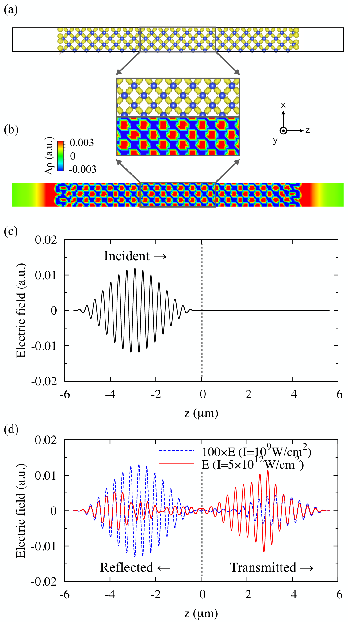
In Fig. 2, we show a typical result of the microscopic Maxwell-TDDFT calculation. The thickness of the Si film is set to nm and the frequency is eV. This frequency is above the optical gap energy of bulk silicon and a strong absorption of the light pulse is expected. We show the results of two different maximum amplitudes, a sufficiently weak case in which a linear response theory is applicable, and a strong case in which nonlinear light-matter interaction is significant. Panel (a) shows the electron density in the ground state. High-density region is seen in the bond region. The electric field of the incident pulse is shown in (c) for the case of the strong pulse. The Si film is placed at position. Since the thickness of the Si film is much smaller than the wavelength of the incident pulse, the Si film is drawn as a dashed line without thickness in the figure.
In panel (d), the electric field after the interaction is shown for two cases. The incident pulse split into transmitted and reflected waves. Blue dotted curves indicate the results of weak pulse case, while red-solid curves show the results of the strong pulse case. The electric field of the weak pulse case is rescaled so that it can be directly compared with that of the strong pulse case. The transmitted wave of the strong pulse case is slightly more intense than that of the weak pulse case. On the other hand, the reflected wave of the strong pulse case is much smaller than that of the weak pulse case. This fact indicates that the nonlinear light-matter interaction for the strong incident pulse manifests in the strong enhancement of the absorption and the strong reduction of the reflection by the Si film.
In Panel (b), the change of electron density from the ground state is shown for the case of strong pulse incidence at the time when the electric field is shown in the panel (d). The density change is shown after averaging over the direction. We can see that the electron density of bonds spreads out and fill the spatial region outside the bonds. The absorbed energy is spent to move the binding electrons and to weaken the bonds.
IV Low intensity case: Linear regime
In this section, we investigate the interaction of a weak light pulse of the maximum intensity W/cm2 with the Si thin films of various thickness. At this intensity, the linear response theory can be applied. As explained in Secs. II.3 and II.4, there are two regimes in which we can introduce macroscopic description utilizing constitutive relations: 2D macroscopic description for the thin limit and ordinary, 3D macroscopic description for the thick limit. We expect the microscopic Maxwell-TDDFT scheme includes both limits and is applied to films of intermediate thickness in which it is difficult to find a macroscopic description utilizing a constitutive relation.
We consider there are two aspects that are important for the linear optical response of thin films. One is the change of the electronic structure in the thin films from that in the bulk. The other is a multiple reflection inside the film. As is easily understood, the microscopic Maxwell-TDDFT scheme takes into account these two features in the formalism, while two macroscopic descriptions, 2D developed in Sec. II.3 and 3D developed in Sec. II.4 are not. In the 2D macroscopic description of Sec. II.3, electronic structure of the thin films can be taken into account through the 2D electric susceptibility of Eq. (24). However, the effect of the multiple reflections is not since we take the zero-thickness limit. In the 3D macroscopic description of Sec. II.4, the effect of the multiple reflections is taken into account, while the effect of the structure changes is not since the bulk electric susceptibility is used.
IV.1 2D electric susceptibility
We first investigate the influences of the changes of the electric structure of thin films from the bulk material on the 2D electric susceptibility defined by Eq. (24). In Fig. 3, we show the 2D electric susceptibilities for the Si films of various thickness. Panels (a)–(d) correspond to films of thickness , , , and , respectively. For comparison, the electric susceptibility of the bulk silicon multiplied by the film thickness, , is also shown. We note that this formula is justified in the thick limit as followsLi and Heinz 2018: If the polarization density is spatially homogeneous inside the film, the 2D polarization density is given by [see Eq. (13)]. Then the 2D electric susceptibility is given by .
A comparison between the 2D and the 3D electric susceptibilities indicates the importance of the structure change as the thickness decreases. As seen from the figure, the difference is very small for sufficiently thick material, . As the thickness decreases, the difference becomes more and more significant. At the thinnest case of in which the thickness is equal to the length of the single cubic cell, the difference is quite significant. We can see that the quantum confinement effect sharpens the peaks in 2–6 eV region. We also find that the nearly zero plateau in the imaginary part appears around 4 eV.
IV.2 Reflection, transmission, and absorption rates
In Fig. 4, we show the reflection, transmission, and absorption rates as a function of the frequency for the weak light pulse irradiating on the Si films of various thickness. We compare microscopic Maxwell-TDDFT calculations shown by red-circles with the rates using 2D and 3D macroscopic descriptions explained in Sec. II.3 and Sec. II.4, respectively.
In the microscopic Maxwell-TDDFT calculations, the rates are calculated using and defined by Eqs. (4) and (5), respectively, at the time fs, immediately after the pulse passed through the film. We will later discuss the time dependence of the rates that indicate the delayed emission (Sec. IV.4).
Here both effects of the changes of the electronic structure and the multiple reflections appear in the comparison. In the 2D macroscopic description, the electronic structure changes are incorporated through the 2D electric susceptibility as shown in the previous subsection, while the multiple reflections are not. In the 3D macroscopic description, while the multiple reflections are correctly taken into account, the electronic structure changes are not. We note that the rates of the microscopic Maxwell-TDDFT calculations are for light pulses which include finite frequency width, while those of the 2D and the 3D macroscopic descriptions are for monochromatic waves.
As seen from the figure, calculations using the 2D electric susceptibility coincide accurately with the microscopic Maxwell-TDDFT calculations for the films of thickness except for the thickest case, . This indicates that the description using the 2D electric susceptibility, Eq. (24), is successful for films of thickness of 5 nm and less. In the case, the absorption using the 2D electric susceptibility is very small compared with the other two calculations. The failure of the 2D description for this case indicates the importance of multiple reflection for that thickness.
The description using the 3D electric susceptibility accurately coincides with the microscopic Maxwell-TDDFT calculations for thicker films, as may be expected. The difference between the three calculations is very small at nm. As the thickness decreases, the difference becomes large, and the calculation using the bulk electric susceptibility is poor for the thinnest case of nm. This is reasonable because the electronic structure of such thin film is very different from the bulk one, as seen in the comparison of the electric susceptibilities.
IV.3 Spatial dependence of energy deposition
To get a better understanding of the mechanism, we investigate the energy deposition, that is, the energy transfer from the light pulse to the electrons in the film. A comparison is made for two calculations, ordinary macroscopic description using the 3D electric susceptibility and the microscopic Maxwell-TDDFT calculations. For the 2D macroscopic description, it is not possible to get such information, since we take the zero-thickness limit.
In the microscopic Maxwell-TDDFT calculation, the energy deposition is given as the derivative of the transmitted energy per area defined by Eq. (3) with respect to :
| (34) |
Figure 5 and Figure 6 show the dependence of and at the time fs at which the incident pulse ends, respectively. Results of the microscopic Maxwell-TDDFT calculation show a rapid oscillation as a function of coordinate, which reflects the atomic layers in the thin film, while the 3D macroscopic calculation is smooth. Except for the thinnest case of , the average behavior of the energy deposition of the microscopic Maxwell-TDDFT calculation coincides with the energy deposition of the 3D macroscopic description. This is consistent with the results of the rates shown in Fig. 4. For the thin films of and , the energy deposition is almost constant in space in the film. This indicates that the electromagnetic fields inside the medium are almost uniform in such very thin film. As the thickness increases, the energy deposition starts to show a decrease as increases. This indicates that the light pulse is attenuated as it propagates through the thin film. At the thickest case of , the energy deposition shows almost exponential decrease.
This finding explains the reason for the failure of the 2D macroscopic description for thick films. The propagation effect becomes significant as the thickness increases, and the spatial dependence of the electric field in the direction becomes sizable for the thickest case of . For such case, the 2D macroscopic description that ignores the spatial dependence cannot be validated.
IV.4 Delayed emission


In the results shown up to here, we used the energy transmission function, of Eq. (3) at the time fs. This means that we calculate the reflection, and the transmission rates shown in Fig. 4 from the electromagnetic fields emitted outside the thin film immediately after the end of the irradiation of the incident pulse.
In the microscopic Maxwell-TDDFT calculation, the energy once stored in the electrons in the medium is re-emitted as light electromagnetic fields, which we call the delayed emission and will be discussed in this subsection. In panels (a) and (b) of Fig. 7 and Fig. 8, we show a vector potential of the reflected and transmitted waves, and , respectively, as a function of time for a long time span. The red solid line and the blue dotted line indicate the microscopic Maxwell-TDDFT calculation and the 2D macroscopic description [Eqs. (18) and (19)], respectively. The thickness of the thin film is , and the average frequency is eV and eV in Fig. 7 and Fig. 8, respectively. We see that the light emission continues a long time after the incident light pulse passes through the thin film. The delayed emission appears both transmitted and reflected waves, and the pulse shapes are very similar to each other. This is understood from the 2D macroscopic description of Sec. II.3. The continuity equation of Eq. (17), , indicates that the transmitted and the reflected waves should be the same after the incident pulsed field ends. The 2D macroscopic result has roughly the same behavior with the microscopic Maxwell-TDDFT result.
In panel (c) of Fig. 7 and Fig. 8, we show a decomposition of the energy of the system. The red-solid lines indicate the electronic excitation energy in the thin film. The blue-dashed line is the energy of the electromagnetic fields outside the computational box area, and the black dotted line is the sum of the two. The summed energy is not completely constant value, because there is an energy of the light electromagnetic fields in the thin film. As seen from the figure, the electronic excitation energy changes into the electromagnetic field in the delayed emission process. We find that the electronic excitation energy, or equivalently, the absorption rate derived by eventually goes to zero in the infinite future. The electronic excitation as well as the delayed emission is much larger in the case of eV, shown in Fig. 7, than those in the case of eV shown in Fig. 8. This can be understood from the 2D electric susceptibility shown in Fig. 3(a). The imaginary part of the susceptibility shows a sharp peak at 3.5 eV, while it is very small at 4.0 eV for the film of thickness.
The emission seen in Fig. 7 is related to the very sharp structure at around 3.5 eV in Fig. 3(a). This indicates the following mechanism for the delayed emission: After irradiating the thin film with a pulse of the average frequency of 3.5 eV, the thin film is highly excited due to the resonant excitation mechanism. Then, through a coupling with the emission channel of the electromagnetic fields, the delayed emission takes place. In fact, taking the Fourier transform of the emitted pulse, it produces a peak at the same energy and the same width as that seen in the 2D electric susceptibility. Therefore, the time scale of the emission is related to the width of absorption peak through the uncertainty principle.
We should, however, note that whether such delayed emission can be observed experimentally depends on the mechanisms of dephasing and decays that take place through the electron-phonon coupling and electron-electron scattering are not taken into account sufficiently in the present scheme.
V High intensity light pulse: Nonlinear regime

In this section, we consider nonlinear interaction in thin materials when an intense and ultrashort light pulse irradiates normally on the material. We first show a systematic view for the nonlinear interaction for the very thin film of thickness using the microscopic Maxwell-TDDFT scheme. In Fig. 9, reflection, transmission, and absorption rates are shown for pulses of various maximum intensities and for several average frequencies. The interaction is in linear regime below the intensity of W/cm2, where the rates do not depend on the intensity. Above W/cm2, the rates changes substantially: the reflection and the absorption rates decrease and the transmission rate increases. This indicates that the intense light pulse tends to transmit through the thin film for light pulse of intensities more than W/cm2. Looking in more detail, there is a difference in the intensity at which the nonlinearity starts to appear: For a light pulse of the average frequency 3.5 eV where a strong absorption is seen in the 2D electric susceptibility, the rates start to deviate at the lowest intensity around W/cm2. This suggests the saturable absorption as the origin of the nonlinearity: a sizable transition in a specific orbitals/k-points causes the saturation of the transition due to the lack of electrons in the occupied orbitals and/or the blocking of the unoccupied orbitals.
We next investigate how the macroscopic descriptions work (Fig. 10). We compare three calculations, the microscopic Maxwell-TDDFT, the 2D macroscopic calculation solving Eqs. (15) and (18) simultaneously, and the multiscale Maxwell-TDDFT calculations solving Eqs. (28) and (29) simultaneously, for the films of various thickness.
We first discuss the reflected wave [Fig. 10(a)–(d)]. At the thinnest case of , the amplitude of the reflected wave is very small. The microscopic Maxwell-TDDFT calculation coincides accurately with the 2D macroscopic calculation. This indicates that the 2D macroscopic calculation is reliable for this thickness. On the other hand, multiscale Maxwell-TDDFT calculation fails to reproduce the microscopic Maxwell-TDDFT calculation. This indicates the importance to treat the electronic structure of a very thin material, as discussed in the linear response calculation.
As the thickness increases, three calculations more or less coincide with each other. At the thick limit of , calculations of multiscale Maxwell-TDDFT and microscopic Maxwell-TDDFT show good coincidence with each other. However, the 2D macroscopic calculation fails. Therefore, the 2D macroscopic approach fails for films of a thickness more than 5 nm. These results are very similar to the case of the weak field: The microscopic Maxwell-TDDFT scheme successfully describes the nonlinear interaction irrespective of the thickness of the film. The 2D macroscopic description is successful for films of thickness 5 nm or less. The multiscale Maxwell-TDDFT scheme, on the other hand, successful for films of 5 nm or more.
For the transmitted wave [Fig. 10(e)–(h)], three calculations coincide with each other up to case. In the thickest case shown in Fig. 10(h), the transmitted wave is rather weak and three calculations look different. The microscopic and multiscale calculations look similar at the beginning. However, the difference gradually increases.
VI Conclusion
We have developed a comprehensive and computationally feasible approach for the interaction of an ultrashort light pulse and thin materials of various thickness. Our description is based on first-principles time-dependent density functional theory. In the most comprehensive description which we call microscopic Maxwell-TDDFT scheme, we couple the time-dependent Kohn-Sham equation, the basic equation of the time-dependent density functional theory, and the classical Maxwell equations for light electromagnetic fields using a common spatial grid. We also develop macroscopic descriptions for two limiting cases: two-dimensional macroscopic electromagnetism for extremely thin materials and three-dimensional macroscopic electromagnetism for sufficiently thick materials. Our schemes can be applied even when the incident field is very strong so that the light-matter interaction is highly nonlinear.
We find that the microscopic Maxwell-TDDFT scheme can describe the interaction of light pulses of various intensities with thin films of various thickness. It incorporates effects of electronic structure changes of the thin film from the bulk material in the first principles level, multiple reflection effects at both surfaces of the thin film, and the nonlinear light-matter interaction for strong incident pulses.
We find the two-dimensional macroscopic description works well for films of thickness 5 nm or less, while the three-dimensional macroscopic description works well for films of thickness 5 nm or more.
Acknowledgements.
This research was supported by JST-CREST under grant number JP-MJCR16N5, and by MEXT as a priority issue theme 7 to be tackled by using Post-K Computer, and by JSPS KAKENHI Grant Numbers 15H03674. Calculations are carried out at Oakforest-PACS at JCAHPC under the support by Multidisciplinary Cooperative Research Program in CCS, University of Tsukuba.References
- Kats and Capasso (2016) M. A. Kats and F. Capasso, Laser Photon. Rev. 10, 735 (2016), arXiv:1606.05707 .
- Kelly and Nicholas (1985) M. J. Kelly and R. J. Nicholas, Reports Prog. Phys. 48, 1699 (1985).
- Novoselov et al. (2005) K. S. Novoselov, D. Jiang, F. Schedin, T. J. Booth, V. V. Khotkevich, S. V. Morozov, and A. K. Geim, Proc. Natl. Acad. Sci. 102, 10451 (2005).
- Nair et al. (2008) R. R. Nair, P. Blake, A. N. Grigorenko, K. S. Novoselov, T. J. Booth, T. Stauber, N. M. R. Peres, and A. K. Geim, Science (80-. ). 320, 1308 (2008).
- Britnell et al. (2013) L. Britnell, R. M. Ribeiro, A. Eckmann, R. Jalil, B. D. Belle, A. Mishchenko, Y.-J. Kim, R. V. Gorbachev, T. Georgiou, S. V. Morozov, A. N. Grigorenko, A. K. Geim, C. Casiraghi, A. H. C. Neto, and K. S. Novoselov, Science (80-. ). 340, 1311 (2013).
- Wang et al. (2012) Q. H. Wang, K. Kalantar-Zadeh, A. Kis, J. N. Coleman, and M. S. Strano, Nat. Nanotechnol. 7, 699 (2012).
- Won and Shigekawa (2010) R. Won and H. Shigekawa, Nat. Photonics 4, 882 (2010).
- Krausz and Ivanov (2009) F. Krausz and M. Ivanov, Rev. Mod. Phys. 81, 163 (2009).
- Bonaccorso et al. (2010) F. Bonaccorso, Z. Sun, T. Hasan, and A. C. Ferrari, Nat. Photonics 4, 611 (2010).
- Calegari et al. (2016) F. Calegari, G. Sansone, S. Stagira, C. Vozzi, and M. Nisoli, J. Phys. B At. Mol. Opt. Phys. 49, 062001 (2016).
- Nicoletti and Cavalleri (2016) D. Nicoletti and A. Cavalleri, Adv. Opt. Photonics 8, 401 (2016).
- Saleh and Teich (2007) B. E. A. Saleh and M. C. Teich, Fundamentals of Photonics; Wiley Series in Pure and Applied Optics (John Wiley & Sons, Hoboken, NJ, 2007).
- Pendry (1996) J. B. Pendry, J. Phys. Condens. Matter 8, 1085 (1996).
- Katsidis and Siapkas (2002) C. C. Katsidis and D. I. Siapkas, Appl. Opt. 41, 3978 (2002).
- Zhan et al. (2013) T. Zhan, X. Shi, Y. Dai, X. Liu, and J. Zi, J. Phys. Condens. Matter 25, 215301 (2013).
- Li and Heinz (2018) Y. Li and T. F. Heinz, 2D Mater. 5, 025021 (2018).
- Gupta et al. (2018) S. Gupta, S. N. Shirodkar, A. Kutana, and B. I. Yakobson, ACS Nano , acsnano.8b03754 (2018).
- Runge and Gross (1984) E. Runge and E. K. U. Gross, Phys. Rev. Lett. 52, 997 (1984).
- Casida (2009) M. E. Casida, J. Mol. Struct. THEOCHEM 914, 3 (2009).
- Laurent and Jacquemin (2013) A. D. Laurent and D. Jacquemin, Int. J. Quantum Chem. 113, 2019 (2013).
- Paier et al. (2008) J. Paier, M. Marsman, and G. Kresse, Phys. Rev. B 78, 121201 (2008).
- Yabana and Bertsch (1996) K. Yabana and G. F. Bertsch, Phys. Rev. B 54, 4484 (1996).
- Bertsch et al. (2000) G. F. Bertsch, J.-I. Iwata, A. Rubio, and K. Yabana, Phys. Rev. B 62, 7998 (2000), arXiv:0005512v1 [arXiv:cond-mat] .
- Yabana et al. (2006) K. Yabana, T. Nakatsukasa, J.-I. Iwata, and G. F. Bertsch, Phys. status solidi 243, 1121 (2006).
- Petersilka and Gross (1999) M. Petersilka and E. K. U. Gross, Laser Phys. 9, 105 (1999).
- Calvayrac et al. (2000) F. Calvayrac, P.-G. Reinhard, E. Suraud, and C. A. Ullrich, Phys. Rep. 337, 493 (2000).
- Tong and Chu (2001) X.-M. Tong and S.-I. Chu, Phys. Rev. A 64, 013417 (2001).
- Nobusada and Yabana (2004) K. Nobusada and K. Yabana, Phys. Rev. A 70, 043411 (2004).
- Castro et al. (2004) A. Castro, M. A. L. Marques, J. A. Alonso, G. F. Bertsch, and A. Rubio, Eur. Phys. J. D - At. Mol. Opt. Phys. 28, 211 (2004).
- Otobe et al. (2008) T. Otobe, M. Yamagiwa, J.-I. Iwata, K. Yabana, T. Nakatsukasa, and G. F. Bertsch, Phys. Rev. B 77, 165104 (2008).
- Shinohara et al. (2010) Y. Shinohara, K. Yabana, Y. Kawashita, J.-I. Iwata, T. Otobe, and G. F. Bertsch, Phys. Rev. B 82, 155110 (2010).
- Miyamoto et al. (2010) Y. Miyamoto, H. Zhang, and D. Tománek, Phys. Rev. Lett. 104, 208302 (2010).
- Yabana et al. (2012) K. Yabana, T. Sugiyama, Y. Shinohara, T. Otobe, and G. F. Bertsch, Phys. Rev. B 85, 045134 (2012), arXiv:arXiv:1112.2291v1 .
- Sommer et al. (2016) A. Sommer, E. M. Bothschafter, S. A. Sato, C. Jakubeit, T. Latka, O. Razskazovskaya, H. Fattahi, M. Jobst, W. Schweinberger, V. Shirvanyan, V. S. Yakovlev, R. Kienberger, K. Yabana, M. Schultze, and F. Krausz, Nature i, 86 (2016), arXiv:NIHMS150003 .
- Lucchini et al. (2016) M. Lucchini, S. A. Sato, A. Ludwig, J. Herrmann, M. Volkov, L. Kasmi, Y. Shinohara, K. Yabana, L. Gallmann, and U. Keller, Science (80-. ). 353, 916 LP (2016).
- Troullier and Martins (1991) N. Troullier and J. L. Martins, Phys. Rev. B 43, 1993 (1991).
- Pickard and Mauri (2003) C. J. Pickard and F. Mauri, Phys. Rev. Lett. 91, 196401 (2003), arXiv:0304115 [cond-mat] .
- Varsano et al. (2009) D. Varsano, L. A. Espinosa-Leal, X. Andrade, M. A. L. Marques, R. di Felice, and A. Rubio, Phys. Chem. Chem. Phys. 11, 4481 (2009).
- Ismail-Beigi et al. (2001) S. Ismail-Beigi, E. K. Chang, and S. G. Louie, Phys. Rev. Lett. 87, 087402 (2001), arXiv:0101383 [cond-mat] .
- Mak et al. (2008) K. F. Mak, M. Y. Sfeir, Y. Wu, C. H. Lui, J. A. Misewich, and T. F. Heinz, Phys. Rev. Lett. 101, 196405 (2008).
- Stauber et al. (2008) T. Stauber, N. M. R. Peres, and A. K. Geim, Phys. Rev. B 78, 085432 (2008).
- Matthes et al. (2014) L. Matthes, O. Pulci, and F. Bechstedt, New J. Phys. 16, 105007 (2014).
- Sernelius (2012) B. E. Sernelius, Phys. Rev. B 85 (2012), 10.1103/PhysRevB.85.195427, arXiv:arXiv:1204.6150v1 .
- Yang et al. (2009) L. Yang, J. Deslippe, C.-H. Park, M. L. Cohen, and S. G. Louie, Phys. Rev. Lett. 103, 186802 (2009).
- Iida et al. (2018) K. Iida, M. Noda, and K. Nobusada, J. Phys. Chem. C 122, 21651 (2018).
- Dressel and Grüner (2002) M. Dressel and G. Grüner, Electrodynamics of Solids (Cambridge University Press, Cambridge, 2002).
- Cho (1991) K. Cho, Prog. Theor. Phys. Suppl. 106, 225 (1991).
- Cho (2003) K. Cho, Optical Response of Nanostructures (Springer, New York, 2003).
- (49) M. Noda, S. A. Sato, Y. Hirokawa, M. Uemoto, T. Takeuchi, S. Yamada, A. Yamada, Y. Shinohara, M. Yamaguchi, K. Iida, I. Floss, T. Otobe, K.-M. Lee, K. Ishimura, T. Boku, G. F. Bertsch, K. Nobusada, and K. Yabana, Comput. Phys. Comm. In press, arXiv:1804.01404.
- (50) http://salmon-tddft.jp, SALMON official website.
- Mur (1981) G. Mur, IEEE Trans. Electromagn. Compat. EMC-23, 377 (1981).
- Perdew and Zunger (1981) J. P. Perdew and A. Zunger, Phys. Rev. B 23, 5048 (1981).
- Momma and Izumi (2011) K. Momma and F. Izumi, J. Appl. Cryst 44, 1272 (2011).