All-spin logic operations Magnetoelectronics; spintronics: devices exploiting spin polarized transport or integrated magnetic fields Magnetotransport phenomena; materials for magnetotransport Spin polarized transport
All-spin logic operations: Memory device and Reconfigurable computing
Abstract
Exploiting spin degree of freedom of electron a new proposal is given to characterize spin-based logical operations using a quantum interferometer that can be utilized as a programmable spin logic device (PSLD). The ON and OFF states of both inputs and outputs are described by spin state only, circumventing spin-to-charge conversion at every stage as often used in conventional devices with the inclusion of extra hardware that can eventually diminish the efficiency. All possible logic functions can be engineered from a single device without redesigning the circuit which certainly offers the opportunities of designing new generation spintronic devices. Moreover we also discuss the utilization of the present model as a memory device and suitable computing operations with proposed experimental setups.
pacs
85.75.-dpacs
75.47.-mpacs
72.25.-b1 Introduction
The use of up and down spin configurations of electron as state variables offers new generation of spin dependent electronic devices, suppressing the mainstream of electronics where everything is charge based. Several advantages like much lower power consumption, rapid processing, non-volatility, higher integration densities are expected in the new generation spin-based systems compared to the traditional semi-conducting devices [1, 2, 3, 4]. In last few years major attention has been paid in developing multi-functional devices involving electron spin such as field effect transistor, modulators, decoders and encoders, quantum computers to name a few [1, 5, 6, 7, 8]. The fruitful development of these functional devices needs much deeper understanding of proper spin dynamics.
Nowadays few ideas have been put forward to implement logical operations, more precisely, spin-based logic gates along with the above mentioned functional devices. Most of the proposals for logic applications usually consider spin state for inputs, while output is charge based [9, 10, 11, 12]. That means a spin-to-charge converter is required at least at one stage which definitely diminishes the overall advantage. However, in a recent work Dutta et al. [13] have given a new proposal for realizing spin-based logic devices along with storage mechanism where spin state is considered at every stage of

operation, though further analysis is still required to probe into it completely. Instead of constructing individual spin logic gates it is always beneficial to design programmable logic devices mainly because of the fact that all logic operations can be obtained from a single device and at the same time it reduces net cost. The another key signature is that different logical functions can be programmed and re-programmed to perform several special-purpose logic operations [9, 14, 15, 16] which include half-adder, full-adder, multiplier, spin-switches, etc. The proper utilization of electronic spin states in the development of memory technologies is another active and novel area of interest as it is supposed that spintronic devices are the most suitable candidates for high density and storage performance [10, 13, 1, 14, 17]. The main effort is being paid to design a non-volatile cheap memory device that can offer high storage performance and at the same time can be accessed as fast as possible like random access memories (RAMs) which has not been well established so far to meet the present requirement of electronic industry.
Here we propose a new idea of designing all possible logical operations considering a single spintronic device. It can be programmed and re-programmed for different spintronic operations and suitably engineered for data storage. The basic device setup for achieving logical responses is illustrated in Fig. 1. The alignment of central magnetic site (site-5) plays the pivotal role. For one configuration a set of four different logical operations (OR, NOR, XOR, XNOR) are obtained, while another set of four logical operations (AND, NAND, XOR, XNOR) are exhibited for the other configuration. The output response is examined in terms of net junction spin current (, where being the spin dependent current), and it is defined as high () when whereas for low () output . Qualitatively, output response can also be determined by observing the sign of as is directly involved with this factor where denotes spin dependent transmission probability.
2 Tight-binding Hamiltonian and theoretical prescription
The spin dependent current () through this nano-junction, described within a tight-binding (TB) prescription, is evaluated from two-terminal transmission probability () which we calculate completely analytically. In terms of spin independent site energy (, , , ) and nearest-neighbor hopping (NNH) integral , the TB Hamiltonian of the interferometer sandwiched between S and D reads as
| (1) |
where , are fermionic operators. The spin dependent interaction term is responsible for the separation of up and down spin channels where being the strength of magnetic moment placed at th site (non-vanishing contributions come from the sites 2, 4 and 5 only). Here we assume that (-component of Pauli spin matrix) is diagonal. A similar kind of TB Hamiltonian is also used to describe S and D, except the term as they are non-magnetic, and they are parameterized by NNH strength and site energy . These electrodes are coupled to the metal channel via the coupling parameters and .
To calculate we use transfer-matrix (TM) method [18, 19], a well-known technique for studying transport properties through a conducting junction. First we renormalize the interferometric geometry (central part of Fig. 1) into a linear chain which effectively shrinks to a single bond connecting the parent atomic sites 1 and 3 as shown in Fig. 2.

Under this renormalization the effective site energy () of the sites 1 and 3 and hopping integral () between them read as (considering and eV, to get a simple closed form structure)
where,
| (5) | |||||
| (6) |
In the above expressions denotes the energy, and , and are the strengths of magnetic moments of the magnetic sites placed at , and , respectively. From the Schrödinger equation ( represents the Hamiltonian of the full bridge system, and ) we can write the transfer matrix equation relating the wave amplitudes () at sites , and , as
| (7) |
where represents the transfer matrix of the complete system. and are the transfer matrices for the sites labeled as 1 and 3, respectively, and and correspond to the TMs for the boundary sites at the left and right electrodes, respectively. As the electrodes are perfect the wave amplitude at any particular site gets the form , where ( is the lattice spacing). The wave vector is on the other hand related to the energy as . With this energy expression and considering the above form of wave amplitude we can write the TMs (setting , eV) as follows:
and,
Assuming plane wave incidence for up and down spin electrons Eq. 7 boils down to the following forms for two different spins:
| (8) |
and
| (9) |
where and are the spin-dependent transmission and reflection amplitudes. These are the two primary equations and solving these equations (Eqs. 8 and 9) we get all the required quantities.
Doing somewhat lengthy calculations we eventually reach to the energy dependent up and down spin transmission probabilities as:
| (10) |
| (11) |
Integrating over a suitable energy window, associated with voltage bias , centering the Fermi energy , spin dependent current is obtained from the relation [20]
| (12) |
Finally, net spin current is evaluated from the expression .
3 Essential results
Equations 10 and 11 are the key expressions for analyzing qualitatively the all-spin logic operations in a single device. The results are presented in Fig. 3 for the setup where the magnetic

moment at site is aligned along ve -direction. The full allowed energy window (eV eV) is divided into four equal regions (any two such energy zones are separated by an imaginary dashed vertical line) where each region is associated with a distinct logical

operation (see Fig. 3). For a quantitative analysis of logical operations i.e., in terms of net spin current , we integrate () for a bias window V setting the Fermi energy at the centre of each distinct energy zone. The results
| In-I | In-II | Output ( in A) | |||
|---|---|---|---|---|---|
| NOR | XOR | XNOR | OR | ||
| 1.5 | -11.3 | 11.3 | -1.5 | ||
| -1.5 | 11.3 | -11.3 | 1.5 | ||
| -1.5 | 11.3 | -11.3 | 1.5 | ||
| -10.1 | -4.3 | 4.2 | 10.1 | ||
| In-I | In-II | Output ( in A) | |||
|---|---|---|---|---|---|
| NAND | XNOR | XOR | AND | ||
| 10.1 | 4.3 | -4.3 | -10.1 | ||
| 1.5 | -11.3 | 11.3 | -1.5 | ||
| 1.5 | -11.3 | 11.3 | -1.5 | ||
| -1.5 | 11.3 | -11.3 | 1.5 | ||
are placed in Table 1. Interestingly we see that the output currents are reasonably high (A), and thus easy to detect.
Reversing the orientation of magnetic moment of the central magnetic site (site ) we get another set of four distinct logical operations (see Fig. 4), among them two operations (XOR and XNOR) are common with the previous device setup. Both the qualitative (Fig. 4) and quantitative (Table 2) analysis for getting different logical operations for this case are similar as discussed above and therefore we skip exploring them once again. In addition, it is important to note that by locking the orientation of anyone of the two inputs and altering the direction of the other input, NOT gate operation can easily be achieved as reflected from Tables 1 and 2. Thus, tuning the Fermi energy via suitable gate electrodes [21, 22] and selectively orienting the central magnetic site we can in principle configure all possible logic gates from a single device by measuring the spin current at output electrode. This is one of our primary motivations behind this work.
4 Robustness
Now we discuss the characteristic features which substantiate the robustness of our proposed device in the context of logical operations. (i) First and foremost signature is that different logical operations can be programmed and re-programmed by configuring the setup in a single device. (ii) No spin-to-charge converter is required as every stage of operations is described by only spin states which circumvents the loss of efficiency as usually noticed in earlier propositions. The applicability of all spin states, on the other hand, suggests to construct all possible functional spin-based logic functions like multiplier, half-adder, full-adder, and to name a few. (iii) Magnitudes of output current is reasonably high (A) compared to the predicted nA currents [9], which is thus easy to measure more conveniently. (iv) For experimental realization we need to focus on two important aspects: one is spin injection efficiency and the other is channel system i.e., whether it is semi-conducting or a metallic one. For metal channel efficiency of spin injection is reasonably high [13], but it exhibits less spin coherence length. Whereas for a semi-conducting material though coherence length is considerable, spin injection performance in it is extremely poor. Thus, metallic one is the favorable option provided the issue of coherence is solved, and hopefully it can significantly be managed by considering a smaller system. This is exactly what we do here, since we consider a metallic channel comprising only five atomic sites (too small) out of which spin dependent scattering takes place only from three magnetic sites. (v) As the spin dependent scattering region is separated by NM sites in both sides of S and D, input states are unaffected by the output states that may arise from type interaction which yields feedback elimination and it is an important aspect for designing efficient spintronic device. It is also important to note that the output is determined completely by input states, not by any power supply. (vi) For selective switching of input states efficient mechanism is definitely required. One basic prescription of doing this is the application of local magnetic field [23, 24], such that it does not influence any other part of the device. Here we present an elegant
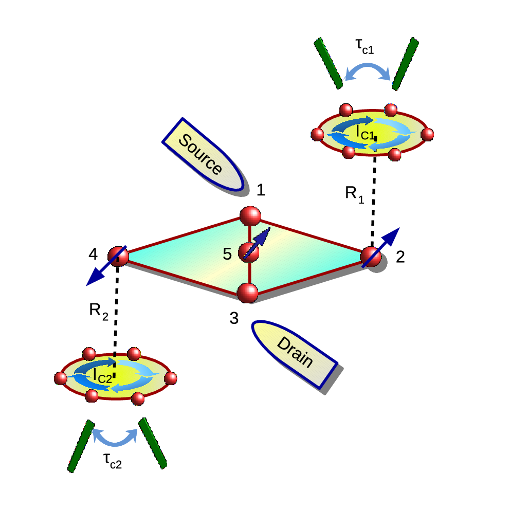
technique incorporating the idea of bias dependent circular current in a nano ring that induces a magnetic field at selective regions with tunable strengths. We will discuss this mechanism elaborately in the next section. (vii) As the size of the bridging conductor is too small energy levels are widely separated, and thus all the logic functions can be performed even at moderate temperatures which is always an important issue for application perspective. (viii) Finally, it is important to note that all the physical pictures studied here are observed for a wide range of bias window and remain invariant under a broad range of parameter values which we confirm through exhaustive inspections. Certainly this feature brings significant impact and confidence in designing an experimental setup along this line.
5 Proposed experimental setup for logic device
A possible experimental setup is demonstrated in Fig. 5. The main concern is associated with the specific alignment of magnetic moments, describing the input states, by a worthy mechanism. The key concept is that in presence of finite bias a net circular current is established and

because of nano sized ring the current induces a strong enough magnetic field [25, 26] which is responsible for orienting the magnetic moment in desired direction. Introducing a shunting path between and , and tuning the hopping strength along this path [27, 28] circular current, and thus magnetic field, can be tuned in a broad range (see Fig. 6) along with phase reversal which might be very helpful to produce suitable magnetic field in appropriate direction. Though this feature (i.e., generation of local magnetic field) is quite common with previous works [23, 30, 31], but in those proposals the change of magnetic field in a wide range is no longer possible, and not such a simpler way. In order to calculate circular current (and hence induced magnetic field) and to tune it by introducing shunting path in individual nano rings placed in the vicinities of magnetic sites 2 and 4 first we need to describe the Hamiltonian of the system i.e., the ring with attached electrodes, and we do it again by a tight-binding framework. Since the TB Hamiltonian of this part and the detailed analysis of circular current along with magnetic field are given in Ref. [29] here we do not repeat the same part once again. The induced magnetic field interacts with the magnetic moment(s) and this term becomes . This is the conventional interaction term (called as exchange interaction) for a magnetic moment placed in a magnetic field. The TB Hamiltonian of the other part i.e., the interferometer is same as given in Eq. 1.
6 Outlines of experimental realization for memory device
Introducing a free magnetic site and maintaining its magnetization direction when the current is off we can construct non-volatile functional memory device.
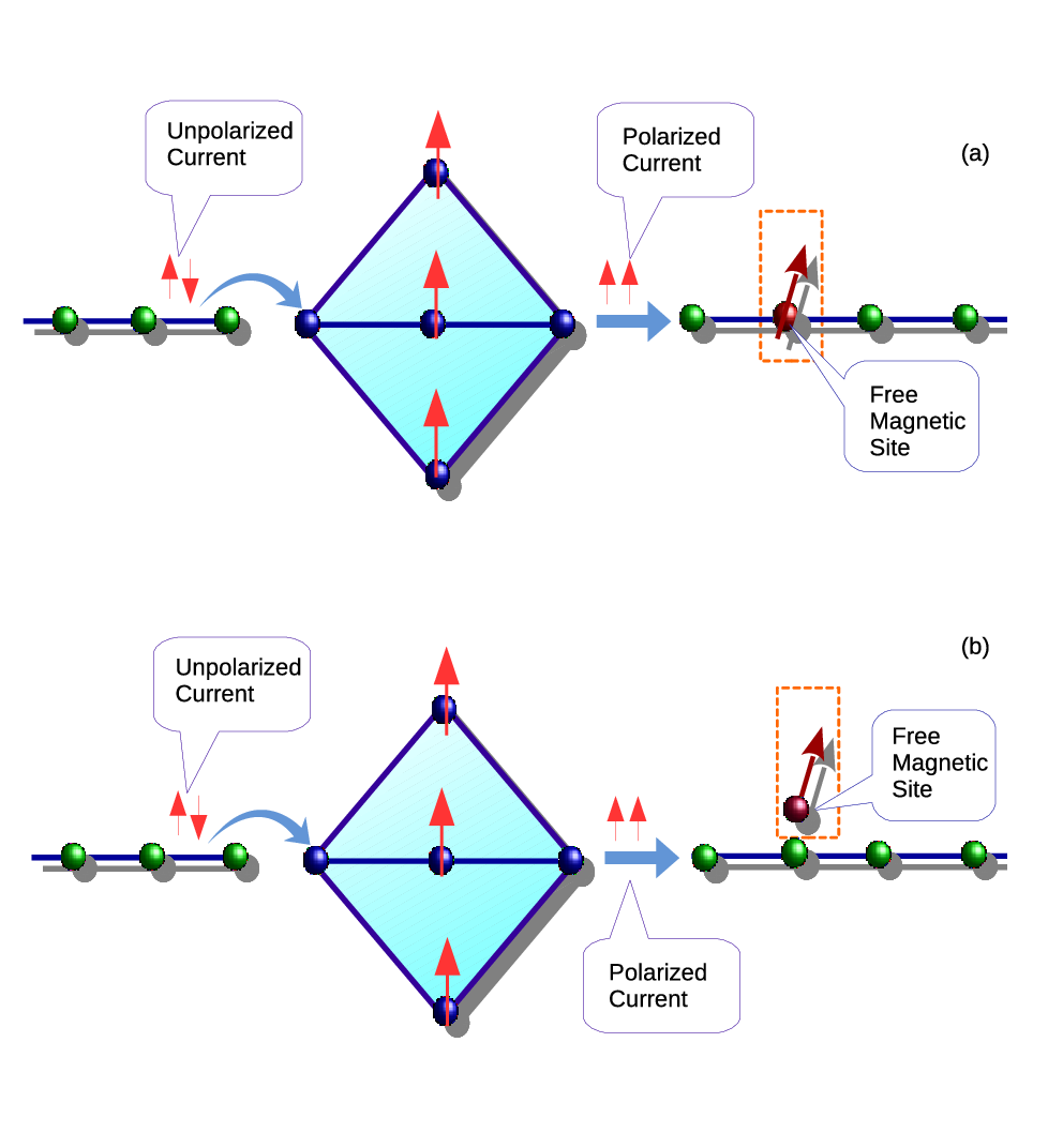
Two different schemes are proposed (Fig. 7) depending on the location of free magnetic site. In the upper panel (Fig. 7(a)) the orientation of free site is adjusted following the mechanism of spin-transfer torque (STT) [32, 33, 34] where spin angular momentum is transferred through exchange interaction, and depending on the sign of polarized spin current, the magnetic moment can be aligned either parallel or anti-parallel to the fixed magnetization direction of the metal channel. Similar prescription (STT) is also applicable to the other setup (Fig. 7(b)) where free magnetic site is not embedded in the drain wire, rather placed very close to it, as electrons can tunnel through this site because of close proximity along with the wired path. Another prescription, the so-called spin-spin exchange interaction, can also be implemented where direct tunneling of electrons through this site is no longer required. For both these two setups the Hamiltonian of the full system can be described by incorporating an extra term in Eq. 1 which reads as where and refer to the magnetic moments of the tunnel electron and free magnetic site, respectively, and corresponds to the interaction strength between these magnetic moments [35]. The main concern in the above two cases is that the physical mechanisms rely on net current transfer through the drain wire and one may think that sufficient current may not be available. But recent intense studies and developments suggest that the required current density, proportional to STT amplitude, to switch magnetization is [32] A cm, and for our model it is too high mainly because of this narrow channel wire. Thus, higher efficiency and improved performance can be expected from our propositions in the development of memory based technologies.
7 Conclusion
We end our discussion by concluding that the proposal studied here provide a boost in the field of storage mechanism, reconfigurable computing, spin-based logic functions and other several spintronic applications.
Acknowledgements.
The authors gratefully acknowledge the valuable discussions with Prof. S. Sil and Prof. J. Ieda. MP is thankful to UGC, India (F. (SA-I)) for providing her doctoral fellowship.References
- [1] \NameWolf S. A. et al. \ReviewScience 294 (2001) 1488.
- [2] \NameNikonov D. E., Bourianoff G. I., Gargini P. A. \ReviewJ. Supercond. Novel Magn. 19 (2006) 497.
- [3] \NameJohnson M. Silsbee R. H. \ReviewPhys. Rev. Lett. 55 (1985) 1790.
- [4] \NameBaibich M. N. et al. \ReviewPhys. Rev. Lett. 61 (1988) 2472.
- [5] \NameZutić I., Fabian J., Das Sarma S. \ReviewRev. Mod. Phys. 76 (2004) 323.
- [6] \NameBader S. D. Parkin S. S. P. \ReviewAnnu. Rev. Condens. Matter Phys. 1 (2010) 71.
- [7] \NamePershin Yu. V. Di Ventra M. \ReviewPhys. Rev. B 78 (2008) 113309.
- [8] \NameOhno H. \ReviewScience 291 (2011) 840.
- [9] \NameDery H., Dalal P., Cywiński Ł., Sham L. J. \ReviewNature 447 (2007) 573.
- [10] \NameNey A., Pampuch C., Koch R., Ploog K. H. \ReviewNature 425 (2003) 485.
- [11] \NameXu P. et al. \ReviewNature Nanotech. 3 (2008) 97.
- [12] \NameBrataas A., Bauer G. E. W., Kelly P. J. \ReviewPhys. Rep. 427 (2006) 157.
- [13] \NameBehin-Aein B. Datta, D. Salahuddin, S., Datta S. \ReviewNature Nanotech. 6 (2010) 266.
- [14] \NameRichter R., Bär L., Wecker J., Reiss G. \ReviewAppl. Phys. Lett. 80 (2002) 1291.
- [15] \NameWang J., Meng H., Wang J.-P. \ReviewJ. Appl. Phys. 97 (2005) 10D509.
- [16] \NameFöldi P., Kálmán O., Benedict M. G., Peeters F. M. \ReviewNano Lett. 8 (2008) 2556.
- [17] \NameLoth S. et al. \ReviewScience 335 (2012) 196.
- [18] \NameMardaani M., Shokri A. A., Esfarjani K. \ReviewPhysica E 28 (2005) 150.
- [19] \NameDey M., Maiti S. K., Karmakar S. N. \ReviewEur. Phys. J. B 80 (2011) 105.
- [20] \NameDatta S. \BookElectronic transport in mesoscopic systems \PublCambridge University Press, Cambridge \Year1997.
- [21] \NameChen J. et al. \ReviewPhys. Rev. Lett. 105 (2010) 176602.
- [22] \NameYu Y.-J. et al. \ReviewNano Letters. 9 (2009) 3430.
- [23] \NameLidar D. A. Thywissen J. H. \ReviewJ. Appl. Phys. 96 (2004) 754.
- [24] \NameTagami K. Tsukada M. \ReviewCurr. Appl. Phys. 3 (2003) 439.
- [25] \NameRai D., Hod O., Nitzan A. \ReviewJ. Phys. Chem. C 114 (2010) 20583.
- [26] \NameRai D., Hod O., Nitzan A. \ReviewPhys. Rev. B 85 (2012) 155440.
- [27] \NamePatra M. Maiti S. K. \ReviewSci. Rep. 7 (2017) 14313.
- [28] \NameXiong Y.-J. Liang X.-T. \ReviewPhys. Lett. A 330 (2004) 307.
- [29] \NamePatra M. Maiti S. K. \ReviewSci. Rep. 7 (2017) 43343.
- [30] \NamePershin Yu. V. Piermarocchi C. \ReviewPhys. Rev. B 72 (2005) 245331.
- [31] \NameMaiti S. K. \ReviewJ. Appl. Phys. 117 (2015) 024306.
- [32] \NameLocatelli N., Cros V., Grollier J. \ReviewNat. Mater. 13 (2014) 11.
- [33] \NameRalph D. C. Stiles M. D. \ReviewJ. Magn. Magn. Mater. 320 (2008) 1190.
- [34] \NameEditorial. \ReviewNature Naotech. 10 (2015) 185.
- [35] \NameRai D. Galperin M. \ReviewPhys. Rev. B 86, 045420 (2012).