Characterisation of SiPMs
Abstract
Silicon photomultipliers, thanks to their excellent performance, robustness and relatively simple use, are the photon-detectors of choice for many present and future applications. This paper gives an overview of methods to characterise SiPMs. The different SiPM parameters are introduced and generic setups for their determination presented. Finally, ways to extract the parameters from the measurements are discussed and the results shown. If a parameter can be obtained from different measurements, the results are compared and recommendations given, which is considered to be the most reliable. The characterisation of SiPMs, in particular for high light intensities and in high radiation fields, is presently a field of intensive research with many open questions and problems which will be discussed.
Keywords:
Silicon photomultiplier , characterisation , gain , break-down voltage , cross-talk , after-pulse , dark-count rate , non-linearity1 Introduction
In this contribution an overview of different methods of characterising SiPMs is given. After a short discussion of the most relevant parameters and their relation to the electrical parameters of SiPMs, generic measurement setups are presented. Finally, methods how the SiPM parameters can be determined with the different setups are presented, and their advantages, disadvantages and limitations discussed.
Several groups have developed methods of characterising SiPMs and most of them are well documented in publications. As it is not possible to do justice to all this work, only generic setups and analysis methods are presented. One complication is that the different groups use different symbols for the technical terms. In addition, these are not always clearly defined. The next section is an attempt to give clear definitions and to summarise the symbols used in this paper in a table. Clearly a common nomenclature is more than welcome, and efforts towards this goal are important for the advancement of the field [1].
The emphasis of the paper is on the characterisation of Analog SiPMs, on which most of the work has been done so far. This in no way means that the development of Digital SiPMs is not appreciated by the author. In fact the opposite is true, and given the impressive developments of microelectronics and 3-D integration, Digital SiPMs may well surpass in the future Analog SiPMs in many applications.
The paper does not cover the excellent timing performance of SiPMs and its measurements, which however is discussed in other articles of this Special Issue ([2, 3, 4, 5]).
As this is a review paper, most of the results are based on discussions with colleagues or on published papers, for which the sources are quoted. If no reference is given, the results are from measurements by members of the Hamburg Detector Laboratory with the analysis performed by the author. Most of these studies used SiPMs produced by KETEK, as for these devices we have access to the technological information to perform simulations.
2 SiPM parameters
Silicon Photomultipliers, also referred to as SiPM (Silicon photomultiplier or Silicon Photo Multiplier), MPPC (Multi Pixel Photon Counter) or G-APD (Geiger Mode Avalanche Photo Diode, which however is mainly used for single pixel devices) are two dimensional arrays of 100 to several 10 000 single photon avalanche diodes (SPAD), called pixels, with typical dimensions between and . The pixels are operated in limited Geiger mode and every pixel gives approximately the same signal, independent of the number of photons which have produced simultaneously electron-hole pairs in the amplification region of the pixel. The sum of the pixel signals is proportional to the number of pixels with Geiger discharges, from which the number of incident photons is deduced. As the output charge for a single Geiger discharge is typically larger than elementary charges, 0, 1, 2, and more Geiger discharges can be easily distinguished, enabling the detection of single optical photons with high efficiency and sub-nanosecond timing.
Two types of SiPMs have been developed: Analog and Digital. In Analog SiPMs the individual SPADs are connected via quenching resistors to a common readout and the SiPM delivers the summed analog signal. In Digital SiPMs each pixel has its own quenching circuit and a digital switch to a multi-channel readout system. The output is the digitised pulse height and precise time information for the pixels with Geiger discharges. Digital SiPMs also allow disabling pixels with high dark-count rates.


The basic functioning of a SiPM, as well as the terms required for its description are explained with the help of Fig. 1, which shows an example of a possible cross section of a single pixel and the electrical diagram used by the author to simulate the pulses for a SiPM with pixels. More realistic pixel layouts are discussed in Ref. [3]. Different to Fig. 1(b), in most of the literature (e. g. Refs. [2, 3, 4]) a voltage source with a value of the break-down voltage is implemented in series with the switch and the resistance , or more general, the switch and the resistor are replaced by a time dependent current source. Which of the models is the more appropriate one, is at present an open question.
The terms used and the corresponding symbols are summarised in Table 1. Fig. 2 shows examples of pulses from single Geiger discharges for a SiPM from KETEK with (a) a pixel size of 25 , and (b) of 50 .
Each pixel is connected to the power supply () by the quenching resistance . Parallel to there is a capacitance . It is the parasitic capacitance of the quenching resistor to the Si-bulk of the pixel and can be intentionally increased to produce a narrow initial pulse allowing a better signal extraction. The capacitance of the diode corresponding to a single pixel is denoted by . is the shunt resistor which converts the current signal into a voltage, which is sensed by the readout. The photon enters the SiPM through a window, which is typically covered by an anti-reflective coating (ARC). The ratio of the area of the entrance window to the pixel area is usually called fill factor, .
The SiPM is biased by a voltage above the breakdown voltage : . In the quiescent state no current flows through and the voltage over the pixel is . An (electron hole) pair, produced either thermally, by a photon or by ionising radiation, initiates with the trigger probability a Geiger discharge by avalanche multiplication. is a function of the position where the pair is generated. A quantitative model for this dependence is given in Ref. [6]. The discharge takes place through a narrow (m diameter) micro-plasma tube until the turn-off voltage is reached, when the multiplication is too low to maintain the micro-plasma. In the electrical model shown in Fig. 1(b) the switch is closed at the start of the Geiger discharge, is discharged through , and the switch opens when . The observed differences are small ( V) and frequently compatible with zero, and in most of the literature just is used. The only paper which reports a significant difference is Ref. [7], and Ref. [8] presents a model calculation of a Geiger discharge and derives a formula for . The time constant of the pixel discharge is short compared to 1 ns. It is responsible for the fast rise time of the output pulse seen in Fig. 2(b). As discussed in Refs. [9, 10] the decay of the measured pulse has two time constants: a fast one and a slower one . describes the recharging of the pixel after the switch in Fig. 1(b) has opened at the end of the Geiger discharge. is associated with the shunt resistance and the total capacitance seen by the amplifier. The total charge of the SiPM pulse is , and the voltage at the peak . The latter formula assumes that the bandwidth of the readout is sufficiently high not to degrade the signal, which is a quite challenging requirement. From Fig. 2 one sees that, contrary to the SiPM with 50 m pixels, there is no evidence for a fast component for the 25 m SiPM. It is concluded that in the latter case .


A parameter which is of particular relevance for the characterisation of SiPMs is the gain
| (1) |
The elementary charge is denoted . If the entire signal is integrated, the gain is . An integration window which is shorter than the pulse or pulse shaping by the readout electronics, result in a gain, , which is reduced by a factor .
As shown in Fig. 3, SiPM charge spectra measured in the dark and with low-intensity pulsed light, show peaks which correspond to , the number of pixels with Geiger discharges. The lowest peak corresponds to , and the following to , 2, etc., with the distance between the peaks . Following the convention from vacuum photomultipliers, it is customary to show charge spectra in units of photo-electrons (pe), by scaling the Q axis by and shifting the scale so that the peak is at zero. As a result the , 2, … peaks are at pe = 1, 2, … , independent of the value of . This is also valid if, instead of the charge, the amplitude of the SiPM signal is analysed.


Another important parameter of a photon detector is the photon-detection efficiency, . For a SiPM it is defined as the ratio of primary Geiger discharges due to the photons, , to the number of photons hitting the SiPM, :
| (2) |
where is the fill factor (ratio of sensitive area to total area), the efficiency of a photon with wavelength entering the sensitive SiPM volume and producing an pair there, and the probability that the pair triggers a Geiger discharge. A primary Geiger discharge can produce correlated secondary Geiger discharges, which can be described by the excess charge factor, , and the excess noise factor, , which are defined below. From the measured mean charge , the number of primary Geiger discharges, , can be obtained using:
| (3) |
For an absolute determination of the absolute value of , and have to be known. The relative dependence of can be obtained more easily from the measured charge spectrum recorded at different values, as discussed in Sect. 4.4.
An ideal photon-detector produces signals with identical shapes linearly scaled with the number photons which have initiated Geiger discharges, and the charge spectrum will consist of - functions at 0, 1, 2, … pe. SiPMs however show a number of differences from an ideal detector, frequently called nuisance parameters. These are:
- 1.
Dark counts produce background signals at the primary dark count rate, .
- 2.
Secondary photons produced during Geiger discharges can generate an electron-hole pair in an adjacent pixel and cause a Geiger discharge there, which results in a double-size signal (d in Fig. 4(a)). This effect is called prompt cross-talk, and its probability is .
- 3.
Secondary photons produced in Geiger discharges can generate an electron-hole pair in the non-depleted Si and charge carriers can diffuse into the amplification region of a neighbouring pixel, where they cause a Geiger discharge. This effect is called delayed cross-talk, and its probability is .
- 4.
During the Geiger discharge, charge carriers can be trapped in defect states and released after some time causing a Geiger discharge in the same pixel as the primary discharge. This effect is called after-pulsing (s+a+a in Fig. 4(a)). The trapping probability for a state is called and the corresponding time constant . As can be seen from Fig. 4(b) the signal strength of after-pulses depends on the recovery state of the pixel, and increases proportional to . In addition, secondary photons generating electron-hole pairs in the non-depleted Si with charge carriers diffusing into the same pixel as the primary Geiger discharge, contribute to after-pulses. This is called optically-induced after-pulsing.
In addition, pixel-to-pixel gain variations and read-out noise will result in signal fluctuations.


The effects discussed above can also be observed in the charge () spectra recorded with a QDC (Charge-to-Digital-Convertor). Fig. 3(a) shows the charge spectrum for a KETEK SiPM with a pixel size of 15 m at V measured in the dark using a CAEN QDC. The peak around 380 QDC channels corresponds to zero, and the peak at 550 QDC channels to a single Geiger discharge. Double and triple Geiger discharges are also visible. The width of the zero discharge peak is caused by the electronics noise. The single Geiger discharge peak is caused by dark pulses which significantly overlap with the 100 ns gate used for the measurement. The tail to the left of the single discharge peak and the flat part between single and zero peak are due to dark pulses which only partially overlap with the gate. The curve Fit 2 is the result of the fit to the data by a model which includes the nuisance effects enumerated above (Ref. [11]). Fit 1 considers only single dark counts without correlated noise.
Fig. 3(b) shows the spectrum for the same KETEK SiPM illuminated by a sub-nanosecond laser pulse. The laser intensity was tuned to result in approximately 1.3 primary Geiger discharges per pulse. As discussed in Ref. [12], and also observed in the spectrum shown, the number of events in the peaks does not follow a Poisson distribution, which is expected for an ideal photon-detector if the incoming photons are also Poisson distributed. The observed number of pulses at high significantly exceeds the Poisson expectation, which is ascribed to prompt and delayed cross-talk. The statistics of cross-talk, which can be described by a Generalised Poisson distribution, is discussed in detail in Ref. [12]. The events in-between the and the pe peak are again ascribed to dark counts. The events in-between the following peaks and the background below the peaks are ascribed to after-pulses and delayed cross-talk. The shape of the spectrum depends on the integration time of the readout electronics, in particular, if only a fraction of the signal is integrated. The curve in Fig. 3(b) is the model fit described in Ref. [11], which includes effects 2–4, but not 1, which explains the disagreement around channel 450. Note, that fitting separately the peaks with Gauss functions and ignoring the background in-between, which is frequently done, does not give the correct number of Geiger discharges, in particular for high values.
The effect of the nuisance parameters is to change the measured distribution with respect to the distribution of converting photons, which would be the response of the ideal photon detector. Two parameters, the excess charge factor, , and the excess noise factor, , are frequently used to describe the worse performance of a non-ideal detector [13]. They are discussed next. The distribution of photons and the number of primary Geiger discharges, , are assumed to follow a Poisson distribution with the mean and the root-mean-square (rms) deviation . The response of the ideal photon-detector will just be the Poisson distribution multiplied with resulting in the mean and the rms deviation . If the measured charge distribution of the real photon-detector has the mean and the rms deviation for the same number of primary Geiger discharges as the ideal detector, then by definition
| (4) |
and
| (5) |
As the contribution of the nuisance effects to the measured signal depends on the effective integration time, also , and depend on the readout and the analysis method used, which presents a significant complication. It should also be noted that assuming a Poisson distribution for the photons producing primary Geiger discharges is not necessarily correct for all light sources.
Non-linearity and saturation are other limitations of SiPMs. As the charge from a single pixel is approximately the same for one and more than one simultaneous Geiger discharge, the signal is expected to saturate at for high number of photons, . The saturation can be described by a decrease of the photon-detection efficiency, , because of the already busy pixels. Well below saturation, the mean number of Geiger discharges is approximately given by , with the photon-detection efficiency without saturation effects . For high numbers of simultaneous photons
| (6) |
is expected because of multiple Geiger discharges in individual pixels. This relation is only valid if the photons are uniformly distributed over the SiPM. If this is not the case, the non-linearity sets in already at lower values and the functional form is different. If the arrival time of the photons is spread over time, some of the pixels will have already partially recovered when the next photon arrives, and signals exceeding are expected, and actually observed. The situation is quite complex, however phenomenological parametrisations are available, which describe detailed measurements [14]. High dark count rates, e. g. due to radiation damage, also cause a decrease of due to pixels in the recharging state after Geiger discharges. This topic is addressed in Sect. 4.6 and in the contribution on radiation damage of this Special Issue [15].
For the description of the nonlinearity, the terms Linearity, Nonlinearity and Dynamic Range are frequently used. Note that different definitions are found in the literature. For the linearity, , a minimum and a maximum value of the number of photons to be detected, and , have to be defined. Then , with the Responsivity . The non-linearity is just . For the dynamic range, values for and for have to be specified. The ratio of where the specified is reached to is defined as the dynamic range. In the situation where zero and one Geiger discharges can be distinguished, appears to be a reasonable convention.
| Symbol | Parameter | Measurement |
|---|---|---|
| Bias voltage | – | |
| Breakdown voltage | ||
| Turnoff voltage | ||
| Overvoltage | ||
| Dark current | ||
| Current with illumination | ||
| Photo current | ||
| Measured charge (amplitude) | ||
| Mean | ||
| Variance of | ||
| Number of pixels | – | |
| Quenching resistance | ||
| Quenching capacitance | ||
| , () | Pixel capacitance | |
| Shunt resistor readout | – | |
| Pixel discharge current | – | |
| Pixel discharge resistor | – | |
| Voltage drop over pixel | – | |
| Capacitance seen by readout | – | |
| Time const. fast component | ||
| Recharging time const. | ||
| SiPM overall gain | ||
| Fraction SiPM signal recorded | ||
| Measured gain | ||
| Number of photons on SiPM | – | |
| Photon-detection efficiency | ||
| in linear range (low ) | ||
| Fill factor | – | |
| Quantum efficiency | – | |
| Geiger breakdown probability | – | |
| for photons | – | |
| Number Geiger discharges | ||
| Number primary Geiger discharges | ||
| due to photons | ||
| pe | Unit Geiger discharges, (photo-electrons) | |
| Fraction events in peak | ||
| in the dark | ||
| with light | ||
| Fraction events above 0.5 pe | ||
| Fraction events above 1.5 pe | ||
| Dark count rate | ||
| Primary | ||
| Probability prompt cross-talk | ||
| Probability delayed cross-talk | ||
| After-pulse probability | ||
| Excess charge factor | ||
| Excess noise factor | ||
| Linearity | ||
| Non-linearity | ||
| Dynamic range | ||
| Responsivity |
3 Measurement setups
In this section an overview of different setups used for characterising SiPMs is presented, and some recommendations given.
3.1 and setup
Fig. 5 shows a schematic layout of the measurement setup used for the and measurements. They are best performed on a temperature-controlled chuck in a light tight and electrically shielded box. As it has been observed that SiPM parameters can be influenced by humidity, a humidity measurement and control of the atmosphere in the box is recommended.
For the measurements the ramping of the voltage should be sufficiently slow so that stable conditions at the individual voltage steps are reached. This can be verified by taking data ramping the voltage up and down. For the precise ( mV) determination of the breakdown voltage , a voltage step around of 100 mV is recommended. This small step size should already be used well below (e. g. 3 V), to avoid problems with fitting the data or numerically calculating derivatives. In addition, note that the Keithley voltage source, which is typically used for the measurements, has a setting accuracy of mV with a saw-tooth deviation as a function of voltage. This can cause problems for a precise determination of . Last but not least, the possibility to illuminate the SiPM with DC light is highly recommended. For low dark currents, (e.g. at low operating temperatures), this is needed for a precise determination of , and for highly irradiated SiPMs with high pixel occupancies, the comparison of the difference of the current with and without illumination for different radiation fluences can give a first idea on the degradation of the SiPM as photon-detector due to radiation damage (Ref. [15] and Sect. 4.6).

The measurement of the admittance as a function of frequency, , can be used to determine the SiPM electrical parameters. In addition to those already described in Fig. 1(b), these are an effective inductance for the biasing lines, and to parameterise the SiPM dark current. Note that in this model the capacitance of the voltage distribution grid in parallel to , discussed e.g. in Refs. [16, 17], is not included. As will be shown in Sect. 4.1 this model gives a fair description of the measured data. For the measurements a large frequency range, e. g. Hz to 2 MHz should be chosen with about 3 -values per decade. High frequencies are in particular relevant for the determination of . Only at high frequencies a significant fraction of the AC-current flows through and its effect can be seen in the measurements. Experience has shown that a value of between 0.5 and 1 V below gives reliable results, even if the dark-count rate is very high (> 1 GHz). As discussed in Sect. 4.2, measurements can be used to estimate the doping profile and the electric field of the avalanche region.
3.2 Current-transient setup
A number of groups (e.g. [13, 18, 19]) are using setups to characterise SiPMs by recording the current transients. They all follow a similar design: The SiPM is mounted in a temperature-controlled chamber, where it can be uniformly illuminated by a sub-nanosecond pulsed light source. The SiPM signal is amplified by a low-noise high-bandwidth amplifier and the waveform digitised by a digital oscilloscope or digitiser. A PC is used for steering the measurements, for storing the data and for performing a first on-line analysis. Fig. 6 shows the setup at FBK as an example. Details can be found in Ref. [13]. Together with this setup a complete analysis chain has been developed which allows a fast and reliable characterisation of large samples of SiPMs. It should be noted that, if such a setup is used to investigate highly-irradiated SiPMs where the dark current can exceed tens of mA, the heating of the SiPM is significant and the exact knowledge of the SiPM temperature is quite a challenge. In addition, the voltage drop over the protection, filter and readout resistors has to be taken into account. Such effects can be investigated using a non-irradiated SiPM and simulating the high DCR by an additional DC light source. To the author’s knowledge, such a study has so far not been reported.

The recording of the transient allows for a most complete characterisation of SiPMs: In the off-line data analysis, pulse amplitudes and time delays of pulses correlated with the primary discharges can be investigated, as well as charge and amplitude distributions for different pulse integration times and digital pulse shaping evaluated. However, the effort to set up a system with low noise, high performance and precise temperature control is significant and requires quite some expertise.
3.3 Charge-measurement setup
Recording charge spectra from SiPMs is significantly simpler than recording and analysing current transients. However, the time information, required for a detailed understanding of the nuisance parameters, is not available. Again a number of groups (e.g. [20, 21, 22, 23, 24]) have set up such systems. An example from Ref. [23] is shown in Fig. 7. A pulse generator triggers a LED, which illuminates the SiPM. The SiPM signal is amplified by a factor 50 (for a load) by a high-bandwidth amplifier and recorded by a Charge-to-Digital-Convertor (QDC) with the gate generated by the pulse generator.

In addition to home-built systems, several firms offer SiPM evaluation kits. An example is the SiPM Educational Kit from CAEN [24]. A photo of such a setup is shown in Fig. 8. It consists of a LED emitting light of 400 nm with sub-nanosecond rise time and 5 ns decay time, a two-channel power supply-amplifier unit and a two-channel 250 MS/s digitiser with 12 bit dynamic range. The firmware allows charge integration, pulse-shape discrimination and triggering. In this way high-speed recording of charge spectra is possible. Commercial and custom built systems, which record charge spectra, are particularly well suited for the high-throughput characterisation of SiPMs.

3.4 Absolute PDE setup
For measuring the photon-detection efficiency, , the response of the SiPM is compared to the response of a calibrated photo-detector. Both pulsed and DC measurements, or a combination of both are used. Again, several setups (e.g. [13, 19, 21, 25, 26, 27]) following similar concepts are in use. As an example, the layout from Ref. [21] is shown in Fig. 9.


As light sources pulsed laser diodes and LEDs with pulse widths below 2 ns are used. The wavelength spectra have a FWHM of typically 5 nm for the laser and 10 to 20 nm for the LED. The SiPM output signal is amplified by a fast amplifier and digitised by a QDC with an integration gate of 50 to a few 100 ns depending on the SiPM pulse shape. Dark spectra and spectra with pulsed light are recorded. The light intensity is adjusted so that the fraction of events without a SiPM pulse, , can be determined precisely. Assuming Poisson statistics for the number of dark counts and of primary Geiger discharges, the mean number of primary Geiger discharges per pulse from the photons of the light source is
| (7) |
with the fraction of events without a SiPM pulse under dark conditions. When deriving this formula the fact is used that in the absence of a Geiger discharge, there are no correlated pulses, and the mean number of primary discharges for both light and dark condition is obtained from the zero probability of the Poisson distribution: . Finally, the absolute is obtained by normalising to the power measured by the calibrated reference diode and , the measured power ratio of port 1 to port 2 using
| (8) |
with the laser repetition rate and the photon energy .
The for typically four wavelengths is determined as described above. In order to extend the measurements to wavelengths in the range between 300 and 1000 nm, a Xe lamp with a monochromator is used as light source and the current from the SiPM and the reference diode is measured. As the current includes cross-talk and after-pulses, the measurements have to be normalised to the measurements described above. With a careful control of different systematic effects, absolute values with an % uncertainty for wavelengths between 350 and 800 nm have been determined [19]. For lower wavelengths the uncertainties are dominated by stray light, and above 800 nm by the knowledge of the quantum efficiency of the Si reference diode. In Ref. [28] a precision method with two integrating light spheres is presented. In Ref. [29] a double attenuator techniques is described which achieves an absolute uncertainty below 0.5 % at a wavelength of 770 nm.
3.5 Counting methods
An elegant method for a quick determination of the nuisance parameters and correlated noise, is described in Ref. [21]. The schematic layout is shown in Fig. 10(a).


The measurements are performed in the dark. Fig. 10(b) shows the count rate as function of the discriminator threshold in units of pe, the amplitude of a single Geiger discharge. The curve, which corresponds to the cumulative pulse-amplitude distribution, shows characteristic plateaus at 0.5, 1.5, and 2.5 pe. The rate for 0.5 pe gives the , and the ratio approximately the overall cross-talk probability.
For the measurement of the time dependence of the delayed correlated pulses, the discriminator threshold is set to a value well above the electronics noise and the time between triggers is measured using the TDC. The measured time distribution can be fitted by the sum of delayed pulses with two time constants and the dark-count contribution. More details are given in [21] noting that the functions used for the fits (Eq. 5 and 6 in the Ref.) are only approximately correct. A similar analysis with an improved formula is given in Ref. [30].
It should be noted that this and more information can be obtained from the the method using current transients as described in Sect. 3.2, which is probably the reason why the counting method is not widely used.
3.6 Optical observation of Geiger discharges
To study the spatial distribution and extension of Geiger discharges, the author of Ref. [31] uses the setup shown in Fig. 11(a). The method is based on the observation that Geiger discharges emit optical and near-infrared photons, as first shown in Ref. [32] and studied quantitatively in Ref. [33]. In Ref. [34] the light spectrum from a Hamamatsu SiPM has been measured in the wavelength range between 450 and 1600 nm.


In Ref. [31] the SiPM is imaged by a high resolution CCD camera with a sensitivity for photons between 300 and 900 nm. Fig. 11(b) shows the image of a KETEK PM3350T SiPM (50 m pixels) in the dark at C for V and an exposure time of 4 h. Assuming that on average every Geiger discharge produces the same amount of light, the observed light intensity is proportional to . Hot-spots are observed with a light intensity approximately 20 times higher than the average. These high generation rates are explained by the presence of point defects, either of the starting material or generated during the fabrication process. A similar observation has been made in Ref. [35] using a digital SiPM, where individual pixels can be disabled and the of individual pixels measured. Thus, the frequently made assumption, that the distribution of dark counts can be described by a Poisson distribution with the same mean for every pixel, is in strong disagreement with this observation. It may be a better approximation for highly radiation-damaged SiPMs. This however has not yet been demonstrated.
Fig. 11(b) also shows that the hot-spots are fixed in space and that the light spots have a diameter of about 10 m, much smaller than the 50 m pixel size, which allows estimating the diameter of the micro-discharge channels. It is also reported that the diameter of the light spots does not depend on .
4 Determination of the SiPM parameters
In the following, it is described how the different parameters discussed in Sect. 2 can be determined using the setups presented in Sect. 3. Most of the parameters can be determined in several ways. Some comments will be given, which way the author considers to be the most trustworthy. As discussed in Ref. [15], most of the methods cannot be applied if the or the noise is so high that 0, 1, and more Geiger discharges cannot be distinguished. Ideas on how to characterise SiPMs in these situations will be presented.
4.1 Electrical parameters
To illustrate the determination of the electrical parameters, results are presented for 4 different KETEK SiPMs studied in Ref. [7]. Their names and parameters are given in Table 2. They all have an area of 1 mm2, PNCV is a special, single pixel produced by KETEK for testing purposes. It cannot be used as photo-detector for voltages above , because the value of is too low to quench the Geiger discharge.
| PM15 | PM25 | PM50 | PM100 | PNCV | |
| 4384 | 1600 | 400 | 100 | 1 | |
| 15 m | 25 m | 50 m | 100 m | 1 mm | |
| 18 fF | 69 fF | 330 fF | 1.5 pF | 110 pF | |
| 750 k | 500 k | 340 k | 410 k | 130 | |
| < 5 fF | < 10 fF | 25 fF | 155 fF | – | |
| 85 G | 80 G | 70 G | 50 G | 85 G | |
| 14 ns | 25 ns | 100 ns | 620 ns | 14 ns |
The admittance-frequency, , measurements were performed at 0.5 and 1 V below the breakdown voltage for 27 frequencies between 100 Hz and 2 GHz. The LCR-meter used records
| (9) |
with the parallel resistance, , and the parallel capacitance, . The series capacitance, , and the series resistance, , are obtained from Eq. 9 using . For the analysis, the electrical model shown in Fig. 5 with the switch closed, is used. The admittance of a single pixel is given by
| (10) |
and the total admittance by
| (11) |
Fig. 12 shows as a function of frequency the measured and . From Eq. 11 follows that for intermediate frequencies , and at high frequencies, for , . For the SiPMs PM50 and PM100, where a significant fast component is observed in the current transient (see Fig. 2), the decrease of at high frequencies can be seen in Fig. 12(a). At high frequencies, the dominant contribution to is in series with . Thus in Fig. 12(b) at high frequencies the constant value of gives an approximate value of . With these initial values for , , and , all 5 parameters of the model (, , , , ) are adjusted until the data are well described. The results are shown as solid lines in Fig. 12.
It is concluded that the electrical SiPM parameters can be approximately determined from measurements and that with this method the change of these parameters with irradiation can be determined for highly irradiated SiPMs, where dark-count rates exceed GHz. Ref. [36] reports such a study for radiation damage by X-rays, and Ref. [37] by reactor neutrons up to fluences of cm-2. A detailed study of the accuracy of this method and its dependence on the SiPM design has so far not been published. However, it is surprising that this method of determining the electrical SiPM parameters is hardly used.


The standard way of determining is to measure the current for forward bias with a setup as shown in Fig. 5 with the switch closed. For sufficiently high values the diode becomes conductive and the differential resistance is . Examples for such measurements from Ref. [19] are shown in Fig. 13.


Fig. 13(a) shows the results for temperatures between and C with straight-line fits for V. The inverse of the slope gives . Fig. 13(b) shows the temperature dependence of . As expected for a poly-Si resistor, the resistance increases with decreasing temperature.
From the author’s experience, the value obtained for depends on the fit range, and the derivative approaches, but does not reach a constant value. For the KETEK SiPMs studied by the author, the value of from the measurement is typically 5 % higher than the one found from the measurements, which is assumed to be more accurate. However, for the SiPM characterisation the precise knowledge of is not so important.
4.2 Electric field
From measurements it is possible to estimate the doping density and the electric field in the amplification region. Such information, which is only rarely communicated by the vendor to the user, is required to simulate the Geiger breakdown probability as a function of position, which can be done using the formulae given in Ref. [6]. For the determination of the electric field the standard 1-D textbook formulae for an asymmetric junction given e. g. in Ref. [38] can be used:
| (12) |
with the distance from the junction , and the doping density , and
| (13) |
for the electric field . The SiPM area is denoted by , the elementary charge by and the dielectric constant of Si by . The maximal depletion depth reached is , where V is the maximum bias voltage used in the measurements. Fig. 14 shows the results for the KETEK SiPMs of Table 2. For these SiPMs the junction is close to the entrance window, the built-in depletion depth is about m, and the maximal electric field kV/cm for approximately 0.5 V below the breakdown voltage . The full depletion depth is about m, which is quite shallow, and results in a relatively narrow amplification region. The observation, that the electric field obtained for the PNCV, a single 1 mm2 diode, and for the SiPMs with different pixel sizes are approximately the same, confirms that assuming the 1-D model and taking the entire SiPM area for in the analysis, are reasonable for the SiPM investigated. The electric field above can be estimated, by adding to the field determined below .

4.3 Breakdown and turnoff voltage
Consistent with the discussion in Sect. 2, a distinction is made in this paper between , the voltage at which Geiger discharges start to occur, and , the voltage at which the Geiger discharges are quenched. In Ref. [7] a difference of about 1 V is reported for a specific SiPM, and in Ref. [8] a model calculation for is presented. However, in most of the literature only is used, and this issue still has to be clarified. If the SiPM is operated well above , a small difference has only a small effect. However, if the SiPM is operated close to , which may be required at high dark count rates due to background light or radiation damage, the effect could be significant.
Two types of measurements are used to determine the breakdown voltage : Analysis of the characteristics and extrapolation of to . For the determination of the turn-off voltage , the linear gain-voltage dependence, is extrapolated to .
Fig. 15 shows measurements for the KETEK SiPM MP15 at C and C in the dark and with DC illumination by a blue LED with low and high photon intensity. The current scale extends over 9 orders of magnitude. At the currents with and without illumination increase rapidly due to the onset of Geiger discharges. As will be shown later quantitatively, at a given temperature the same value is observed with and without illumination. Between C and C decreases by mV, because of the increase of the charge-carrier ionisation coefficients with decreasing temperature.
Below the characteristics are very different for the data with and without illumination: With illumination () the expected increase in current due to avalanche multiplication – the regime in which Avalanche Photo-Diodes (APDs) are operated – is observed, whereas without illumination () the current is constant up to . The reason is that below is dominated by surface-generation current from the depleted Si-SiO2 interface, which misses the amplification region and is therefore not amplified.
At the current rises rapidly, with an increase which is higher for the illuminated SiPM. The reason is again that charge carriers from the Si-SiO2 interface bypass the amplification region. It is also seen that the relative slope of is steeper than of above . The reason is the position dependence of the Geiger trigger probability, . It is highest close to the junction, which for this SiPM is located near to the SiPM entrance window. Whereas the thermally generated pairs are approximately uniformly generated in the depletion region, the blue light has an absorption length of m and generates pairs in the region of highest only. With increasing the region of high extends further and further into the amplification region, thus increasing for the uniformly generated pairs from dark counts.
At voltages above V, and at C show an increase of the slope of compared to the C data. It still has to be investigated if this increase is due to Geiger discharges for which the quenching is delayed and the current through during the discharge contributes significantly to the signal, or to an increased correlated noise (e. g. after-pulses) at high electric fields and low temperature.
Several methods are used to determine from the measurements giving all similar results, and it is a matter of taste which one to use. Most of them use either the logarithmic derivative, , or its inverse . The advantage of and is that they are only sensitive to the shape and not to the value of , and measurements can be easily compared, even if the current values are vastly different. This is seen in Fig. 16, where and differ by three orders of magnitude, and the s are quite similar.
The breakdown voltage for the different methods is determined as the voltage at which
- 1.
has its maximum.
- 2.
The parabola through the 3 points around the minimum of has its minimum.
- 3.
The extrapolation of a straight-line (or parabola) fit of for is zero.
- 4.
The extrapolation of a straight-line fit of for is zero
- 5.
The second derivative of with respect to has its maximum.
- 6.
A second order polynomial, fitted to above after surface-current subtraction, crosses the axis.
Fig. 16 and Table 3 show the results of methods for the KETEK SiPM PM15. Shown in the figure are and with the scale on the right, and the corresponding results with straight-line fits below and above , with the scale on the left. It is found that the results for from and for agree within mV. The values found from for methods 1 and 2 are systematically higher by mV, which is related to the nearly constant for , which results in a very high value and shifts the minimum to somewhat higher values.
In Ref. [19] method 5 is compared to methods 1 and 2, and agreement at the 100 mV is reported. To the knowledge of the author, a comparison at the 20 mV level is not available. In addition it is noted, that obtaining reliably second derivatives from experimental data can by quite tricky.
As discussed below, the second order polynomial of method 6, which is proposed in Ref. [10] and also recommended in Ref. [19], describes only the but not the data for the KETEK SiPMs. Therefore it was not used. The method assumes the functional form for the Geiger breakdown probability for both and . Apparently the functional form of depends on the SiPM design and is also position dependent. As a result, a power-law fit with the free parameter , which is equivalent to method 3, is the safer approach.
For a quick and reliable determination at the 50 mV level it is recommended to use method 2 with the SiPM illuminated with DC light. In particular at low temperatures is so low that the measurement errors are significant, which makes the results unreliable. An idea about the dominant systematic uncertainties and a more precise determination can be obtained by varying the fit range in method 3 and by using a second order polynomial to fit .
| Method | 1 | 2 | 3 | 4 |
|---|---|---|---|---|
| [V] | 27.6 | 27.57 | 27.42 | 27.44 |
| [V] | 27.5 | 27.51 | 27.49 | 27.41 |
From the fit using method 3 the inverse slope of is obtained: from , and from . The values found for and for are 1.96 and 1.43, respectively. For an dependence, . Thus a straight line of means that above the current obeys the power law
From and information on the position- and -dependence of the Geiger-discharge probability, , can be obtained: Assuming a uniform, voltage-independent thermal volume-generation rate in the depletion region, i. e. ignoring high-field effects, the primary dark count rate = , and , where is averaged over the entire depletion region. In the approximation , , and taking into account that for small values, . The corresponding relation for the photo-current is: , from which follows . Here the average of is taken over the region in which the photons are absorbed, which extends only to m from the entrance window for the blue light used. Thus is related to at the SiPM entrance window, and to in the entire depletion region. This information can be used to validate simulations of the position dependence of for different values.
Another approach of determining is presented in Refs. [19, 39]. The measured voltage dependence of is fitted by the phenomenological function
| (14) |
with the phenomenological parameter . The measurement of the will be described in Sect. 4.4. The values found for agree with the values found using the methods described above, however the uncertainty is significantly larger. The authors point out that in first approximation does not depend on the width of the multiplication region and conclude that the wavelength dependence reflects the position dependence of . These results still have to be compared to simulations using the formulae given in Ref. [6] with realistic electric fields, or TCAD or Monte Carlo programs. In Ref. [7] a similar approach is followed: is fitted with the dependence derived assuming that all electron-hole pairs are generated at the SiPM entrance window and a constant electric field in the depletion region of effective width . The values found for are again compatible with the values using the methods.
The turn-off voltage, , is obtained from the voltage dependence of the SiPM gain, , by fitting a straight line to the data and extrapolating to . Examples for for the KETEK SiPM with pitch values between 15m and 100m and the corresponding straight-line fits are shown in Fig. 17(a). The determination of and of the fluctuations of is discussed in Sect. 4.4.
In Fig. 17(b) the differences for the different pitch values of the KETEK SiPMs are shown. The value from is labeled VI, and the one from , VPD. The symbol used for from is labeled VG. The values found from VI and VPD are compatible, confirming that they both determine . However they differ from the values from VG, which determines . The difference is approximately 1 V for the SiPM with m pixels and decreases with increasing pixel size. The reason for this dependence is not understood, however to the author’s knowledge no simulations with realistic 3-D electric fields have been performed so far.
For the determination of , instead of derived from charge spectra, from the pulse amplitude can also be used. The results obtained are compatible. Given the sensitivity of the amplitude to the band-width of the readout, in particular in the presence of a fast component, this method is not recommended.
In summary: A difference of up to 1 V between and has been observed for a KETEK SiPM with a pitch of 15m. For larger pitch values, the difference decreases. For the gain the relevant voltage is , i. e. . To avoid confusion, in publications it should be clearly stated, which voltage, or , is used.


4.4 Photon-detection efficiency, number of primary Geiger discharges and gain
If peaks corresponding to different numbers of Geiger discharges, , can be separated in the charge or amplitude spectra, the dependence of the relative can be obtained from and from using Eq. 7. Fig 18, taken from Ref. [19], shows the dependence of for a number of wavelengths for two SiPMs. The relative values are obtained with the method described above.
The determination of the absolute uses calibrated photo-diodes, as already discussed in Sect. 3.4. There are several setups, both at producers and at research laboratories, which measure the absolute of SiPMs as function of wavelength and with an accuracy of a few %. Examples from Ref. [19] of the dependence of the absolute are shown in Fig. 18, and of the wavelength dependence at a Geiger-breakdown probability %, in Fig. 19. The accuracy achieved in these measurements is impressive, and so is the increase in achieved by the producers in recent years.


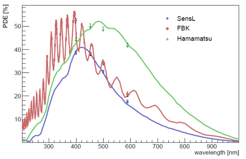
Next, different methods of determining the SiPM gain are discussed. The most straight-forward method of measuring the gain, , of the combined system SiPM–readout, is to record charge spectra, as shown in Fig. 3, and determine the distance between the peaks corresponding to different number of Geiger discharges. Several methods are used:
- 1.
Fit individual peaks by Gauss functions and determine the distance between them.
- 2.
Determine the distance using the Fourier transformed spectrum (Ref. [23]).
- 3.
Perform a complete fit of the spectrum with as one of the free parameter of the fit (Ref. [11]).
All three methods give very precise and compatible results, and it is matter of taste and convenience which one to use. However, they all require that 0, 1, 2, etc. are well separated.
In addition to , the rms width of the peaks corresponding to different number of Geiger discharges, , can be obtained from the spectra. As expected and observed, the data can be described by , with the contribution from the electronics noise and the contribution from the fluctuations of for single Geiger discharges. For the KETEK SiPM investigated in Ref. [11] it is found that has only a weak dependence: Between V and 35 V it increases by % only. For this SiPM V at C. As , there are two contributions to . One from the pixel-to-pixel variations of , called , and one from the fluctuations of , called . The two terms can be distinguished using the dependence of . Using the measured slope and the definition of , one finds:
| (15) |
As is approximately independent of , the second term is small and: , giving mV for the data from Ref. [11]. It is concluded that the increase of the width of the peaks in the SiPM charge (or amplitude) spectra is caused by differences in and not by differences in pixel capacitances. The reason for the rather large value of could be differences of the 3-D electric field distribution within a pixel. To the author’s knowledge, no realistic simulations of and have been performed so far.
If , 1, 2, … peaks can not be separated, the gain, , and the mean number of primary Geiger discharges, , can nevertheless be determined from the mean, , and the root-mean square, , of the measured charge (or amplitude) distribution if the excess charge factor, , and the excess noise factor, , are known. The method is an extension of the well known method used to determine the gain, , and the mean number of photo-electrons, , for vacuum photomultipliers, which are (incorrectly) assumed to be ideal photon-detectors with . For the ideal photomultiplier the distribution of the photo-electrons generated by the pulsed light is assumed to follow a Poisson distribution, for which both mean and variance are equal to . With the gain , the mean of the measured charge distribution becomes , and the square of the rms spread . The subscript , which stands for Poisson, refers to the ideal detector. From these two equations follows:
| (16) |
For a non-ideal SiPM, and , defined in Eq. 4 and 5, have to be taken into account, which results in
| (17) |
| (18) |
where for the SiPM the mean number of photo-electrons of the vacuum photomultiplier, , has been replaced by the mean number of primary Geiger discharges . Solving the two equations for and gives
| (19) |
A method to determine and is presented in Sect. 4.5.
In Ref. [11] the results for and determined by a fit to the charge distribution are compared to the ones from and for the KETEK SiPM with 15 m pitch illuminated with a pulsed LED. Fig. 20 shows the results. For both and the agreement is within a few percent, demonstrating the validity of the method. This method is straight-forward to use and suitable for the in-situ calibration and the monitoring of large numbers of SiPMs. It is used routinely in Ref. [40]. It should be noted that in the case of significant noise, the width of the peak has to be subtracted quadratically from . In addition, it should be mentioned that the method as described does not work if the response of the system SiPM–readout is non-linear. But it is straight-forward to extend the method to non-linear regions, which, however, to the author’s knowledge, has not yet been reported.


4.5 Nuisance parameters: Dark-count rate and correlated noise
Compared to an ideal photon-detector, the SiPM performance is affected by a number of nuisance sources, in particular random dark counts and pulses correlated with primary discharges. The different types of nuisance parameters have been discussed in Sect. 2. The best way to study them in detail, is to record current transients without or with low-intensity illumination. The analysis and results presented in Ref. [19] will be discussed next. The analysis procedure used follows closely the one reported in Ref. [13]. Similar analyses are reported in Refs. [41, 42, 43].
In Ref. [19] the transients are differentiated by subtracting a copy of the transient shifted by 3 ns (see Fig. 21(a)). In this way the pulse tails are removed and the pulses have a full width of about 9 ns. Next the undershoot is removed by applying a background-subtraction algorithm, and pulses with an amplitude exceeding 0.5 pe (pe = the average amplitude of a single Geiger discharge) are marked. Finally pulses corresponding to single Geiger discharges are selected, and the time difference to the following pulse versus its amplitude plotted, as shown in Fig. 21(b). Note that the scale and the bin widths are logarithmic.


Dark counts without correlated noise have an average amplitude corresponding to one Geiger discharge. They appear as horizontal line around pe = 1. Dark-count pulses with one or two prompt optical cross-talk pulses, each with an amplitude of 1 pe, appear as horizontal lines at pe = 2 and 3, respectively. After-pulses have an amplitude which increases with time due to the recharging of the pixel (see also Fig. 4(b)). Pulses with delayed optical cross-talk are the sum of the decaying pulse of the primary Geiger discharge and one or two optical cross-talk pulses, each with an amplitude of 1 pe. Their amplitudes decrease towards pe = 1 or 2 with increasing . By selecting events in the different regions, all nuisance parameters can be determined in a quantitative way. In the following a few examples are given.
The total dark-count rate , , can be approximately determined by counting all pulses and dividing the number by the total duration of all analysed transients. is given by the primary dark count rate plus the effects of after-pulses and delayed optical cross-talk. A more precise procedure is to analyse the distribution, , which for random dark pulses at the rate is expected to have the form . This dependence follows from the properties of the Poisson distribution: The mean number of dark counts () in the time interval is , and the probability of zero s in is . The absolute value of the derivative is proportional to the probability of the change from 0 to s, thus the occurrence of a at . The distribution for random dark counts, when plotted in bins of , is with the maximum at . This can be clearly seen in Fig. 21(b).
Fig. 22(a) shows an example of a distribution with a fit of the expected dependence for ns. At lower values the effects of correlated pulses are clearly visible. In Refs. [21, 30] the distribution in linear scale is fitted to the sum of s and after-pulses with exponential time distributions. If only s and after-pulses are considered, the expected distribution can be derived by replacing valid in the absence of after-pulses and delayed cross-talk, by for one state, with the probability of after-pulses, , and the time constant . Differentiation of with respect to gives the dependence. Fig. 22(b) shows an example of such an analysis from Ref. [30], which shows that the data are well described by the model and that and are determined with good accuracy. Delayed cross-talk can be implemented in a similar way, if a parametrisation for its time dependence is available.


The can also be obtained from charge or amplitude spectra measured without illumination, as the one shown in Fig. 3(a), using the relation
| (20) |
with , the fraction of events with a charge exceeding half the signal of a single Geiger discharge (1/2 pe), and the gate width used for the current integration. As gate and dark pulses are uncorrelated in time, the charge spectrum contains pulses with different overlaps with the gate, resulting in signals between the and the peak. In Ref. [11] it is shown, that only for Eq. 20 is exact. If a lower or a higher threshold than 0.5 pe is chosen, the value for in Eq. 20 has to be decreased or increased with respect to the actual . Thus fitting the peak and using the fraction of events in the peak instead of , which is frequently done, is only approximate and should be avoided. In cases where the tail of the zero-Geiger discharge peak results in a significant fraction of events above 0.5 pe, these events have to be subtracted when determining . It should be noted that after-pulses and delayed cross-talk result in a systematic bias of this determination. It is estimated that the effect is small, but a systematic study is not known to the author.
To summarise: The method is straight-forward and recommended for determining the , but has a bias, which however in most practical cases will be small. For a more precise determination, the method described above should be used.
The methods described so far can only be applied if peaks corresponding to different number of Geiger discharges can be distinguished. Determining when this is not the case, is significantly more complex and a number of assumptions have to be made in the analysis. Fig. 23, which shows current transients with low light for a SiPM before irradiation (a), and after irradiation (b), shows the problem. Whereas in (a) it is straight-forward to analyse the single Geiger discharge pulse, this is impossible for (b), which shows wild fluctuations with amplitudes, which are larger by one order of magnitude. Transients, as shown in Fig. 23(b), can be reproduced by a simple Monte Carlo simulation by adding pulses as shown in Fig. 23(a) randomly distributed in the time interval of the transient, . For estimating in such a situation, two methods will be described. One uses the measured dark current, , the other , the rms of the charge distribution measured without illumination. These methods are discussed in Ref. [44] and used in Ref. [15] to characterise radiation-damaged SiPMs. At high values, can exceed several mA and an AC-coupled readout is typically used, so that the average current is zero and contains no information. In addition, the high current results in a significant power dissipation causing an uncertainty in the knowledge of the SiPM temperature.
is related to to the primary dark count rate by
| (21) |
from which follows
| (22) |
and can be determined from (Sect. 4.1), and from measurements (Sect. 4.3). If the approximation is made, which is valid for , can be obtained using Eq. 22. As is typically , is already a quite good approximation to . An alternative, which is used in Refs. [15, 44] for the study of radiation damage, is to assume that and do not change with irradiation, and determine from the measurements. The validity and accuracy of these assumptions has not been checked so far.
Next, the determination of from the measurement of the rms-spread, , of the charge (or amplitude) distribution measured without illumination, will be discussed. Fig. 24(a) shows charge spectra measured with a gate width ns without illumination for the KETEK PM15 SiPM irradiated by neutrons to different fluences up to cm-2. As discussed in detail in Ref. [15], the dominant effect of radiation damage is the increase of by many orders of magnitude. One sees that first increases with fluence, and above a fluence of cm-2 decreases. For high values many pixels are already busy with Geiger discharges, and this high occupancy is responsible for the decrease of . The formula used to extract from is:
| (23) |
It is derived in the appendix, under the assumption that the SiPM current pulse for a Geiger discharge at time is described by for . An extension to other pulse shapes is straight-forward inserting the functional form of in Eq. 27. To verify the predicted dependence, Fig. 24(b) compares the measured (symbols) to fits by Eq. 23 (solid lines) with and the term in the parenthesis on the left side, as free parameters. The dependence of and on has been neglected in the fits. Up to a fluence of cm-2 the data are well described, and allow to determine with an accuracy of about 10 %. For fluences exceeding cm-2, the quality of the fit worsens because of the high pixel occupancy at high . For low , is dominated by electronics noise, which has to be subtracted quadratically from . If the electronics noise dominates, the method becomes unreliable. A formula, which takes into account the reduction of due to pixels occupied by dark counts, still has to be derived. In order to determine from Eq. 23, assumptions for , and have to be made. For the determination of , when peaks corresponding to different Geiger discharges cannot be distinguished, Eq. 19 can be used. For the determination of and no method is known to the author, if peaks corresponding to different number of Geiger discharges can not be distinguished. However, in most practical cases the problem of merging peaks is either the result of ambient light or of radiation damage. In these cases, and can be measured initially, and the assumption made that the values do not change for the conditions in which the SiPM is finally used. The validity of these assumptions for radiation damage still has to be demonstrated.

In Ref. [15], is determined as a function of the neutron fluence using the measured and Eq. 23, assuming for and the values of the non-irradiated SiPM. The results are compared to the results using Eq. 22, assuming and from the non-irradiated SiPM and the values of from the analyses for the different neutron fluences. In the range of the validity of the method an agreement to better than 30 % is observed, which is considered satisfactory for values exceeding several GHz. A detailed comparison of the methods and their sensitivity to the assumptions used is still missing.
To summarise this subsection on the and determination: If the is sufficiently low and the peaks for different number of Geiger discharges can be distinguished, the different methods, counting the dark-counts in the transients, analysing the time-difference , and the method, are straight-forward and give reliable results. For values approaching or exceeding , the pixel-recharging time constant (typically between 15 and 200 ns), the situation becomes significantly more complicated. Based on ongoing studies, the preliminary conclusion is that for high s using and Eq. 22 is the most reliable method to determine . This method however, requires the knowledge of and . For it is recommended to use , with from (admittance-frequency) measurements for 0.5 to 1 V below . For , can be used, which however is a poor assumption for small values if differs significantly from . If the difference can be determined for a low DCR, then the assumption of a constant difference can be made, and obtained from measurements. To better understand the effects of high , the following study is recommended: For a SiPM, with properties precisely determined using the methods of individual Geiger discharges, different values can be simulated by DC-light of variable intensity illuminating uniformly the SiPM. In this way the different methods can be compared and the most suitable determined.
Cross-talk, after-pulses, ECF, ENF and optimal resolution
Fig. 21(b) shows the 2-D distribution of the time between pulses, , versus pulse amplitude, which allows identifying the different physical effects responsible for the nuisance parameters. Analysing separately the different event classes allows to study their rate and properties. These studies as a function of and temperature are essential for understanding the different effects and proposing technological modifications of the fabrication process to improve the SiPM performance. They also provide input for the development of realistic SiPM models. An example is given in Fig. 22 with the discussion on the extraction of after-pulses and delayed cross-talk.
However, as long as saturation effects can be ignored, for most users the knowledge of , , and as a function of of the SiPMs will be sufficient to characterise the SiPM and determine the optimal operating conditions. These parameters depend not only on the SiPM properties, but also on the readout used. As an example: A shorter integration of the SiPM current, results in a reduction of , and .
The most direct way to determine these parameters uses two charge spectra: One recorded in the dark (), and one with low-intensity light (Q), so that the fraction of events in the peak for zero Geiger discharges can be measured precisely. In the following it is assumed that the mean of the zero-Geiger discharge peak corresponds to zero charge. is obtained using Eq. 20 from the spectrum and from the distance between the peaks of the spectrum, as discussed in Sect. 4.4. The mean number of primary Geiger discharges due to photons from the light source, , is obtained from Eq. 7. is obtained from the ratio of the mean of the measured charge distribution to the expectation for a Poisson distribution , and from the ratio of the square of the rms-spread, , to the Poisson expectation
| (24) |
The rms-spread allows to estimate the contribution of dark counts to the .
To illustrate the use of , the calculation of the operating voltage at which the photon resolution is optimal is presented. Inserting from Eq. 3 into Eq. 17 and 18 one obtains for the relative resolution
| (25) |
Both and increase with . Whereas eventually saturates, continues to increase, and the relative resolution has a minimum. An example of such a dependence is given in Ref. [11]. As both and depend on the effective charge integration time, Eq. 25 can also be used to optimise the readout electronics.
4.6 Non-linearity and saturation
For calorimetric measurements, e. g. in collider and astro-physics experiments or in PET, the dynamic range, i. e. the range of , where precise measurements are possible, is an essential parameter. High gain, high , single photon-detection and high dynamic range are conflicting requirements, which can hardly be achieved simultaneously. In this respect vacuum photomultipliers are superior to SiPMs. A major complication is that all the nuisance parameters discussed so far enter in one way or another into the dynamic range. In addition, the pulse shape is expected to depend on the number of simultaneous Geiger discharges, and because of the pixel recharging time constant, the dynamic range depends on the time distribution of the photons. In spite of the high relevance of the dynamic range, systematic studies so far are quite scarce.
In Ref. [45] light from a laser with a wavelength of 404 nm and a pulse-width of 32 ps has been used to investigate the dynamic range of simultaneously arriving photons, up to a photon intensity at which Geiger discharges would be triggered simultaneously, if the SiPM were linear. Four different SiPMs with 1 mm2 area and , 400, 556 and 560 from Hamamatsu, Photonique and Zecotec were investigated. Measured was the amplitude of the SiPM pulse recorded with a digital scope as a function of the relative number of photons, , called in the paper. is proportional to the current in a PIN photo-diode with a linear response, normalised so that for low light intensities, where the SiPMs are known to be linear. The measurements were performed for values between 0.5 V and 1.3 V. The way has been determined is not reported in the paper. Fig. 25 shows the results. It is observed that at high light intensities for all SiPMs the mean number of measured Geiger discharges, , significantly exceeds the number of pixels, , and does not appear to reach a constant saturation value. Thus the expectation given in Eq. 6 is not observed. Various explanations of this phenomenon are discussed in the paper, but the conclusion is: Up to now, no convincing explanation for this over saturation and enhanced dynamic range could be found.


Note, that it is expected that the pulse amplitude, which was used in the described measurements, depends on the number of Geiger discharges in a pixel. The reason is that micro-plasma tubes in a pixel correspond to resistors in parallel in the electrical model shown in Fig. 1(b), which results in a decrease of the time constant of the Geiger discharge and thus in a higher amplitude of the fast pulse. This effect has been reported in Ref. [46]. Whereas the charge was found to be independent of , the current amplitude increased with . It also should be noted, that the fast component of the pulse has a rise time of typically several tens of ps and a full width below 1 ns. Therefore the measured pulse amplitude is very much influenced by the bandwidth of the readout.
A study with a picosecond laser, however using charge- instead of amplitude-measurements, for four SiPMs from Hamamatsu (m] = 2668/25, 1600/25, 400/50 and 100/100) has been presented by G. Weitzel [47] and S. Krause [48]. The results are shown in Fig. 26. is the number of pixels, the number of Geiger discharges expected in the absence of saturation, and the measured mean number of Geiger discharges. is obtained by scaling so that for low , where the SiPM response is known to be linear. The data were fitted by , where , and the saturation value of for high light intensities. For the SiPMs with m and m pitch, the values found for are significantly larger than 1 and similar to the findings of Ref. [45]. The SiPMs with m pitch shows values compatible with or closer to 1. An explanation for the difference could be the merging of micro-plasma channels from Geiger discharges in the same pixel for small pixels. Clearly, more studies are needed to understand these results.

In Ref. [14] the dynamic range for light pulses of different durations is studied. As light source a LED is used, driven by a computer controlled pulse generator to generate light pulses of up to ns duration and photon numbers hitting the SiPM, , of up to . The SiPMs investigated were fabricated by KETEK with and m, and by Hamamatsu with and m. Fig. 27 shows the dependence of after correction for dark pulses (called ) on . The value of is shown as a dashed line. For the KETEK SiPM the charge was recorded with a 400 ns gate and for the Hamamatsu SiPM with a 150 ns gate. The authors conclude that in the linear range (which extends to ), the response is independent of . For higher values the response increases with , as does the saturation value. The ratio of the saturation value to for the SiPM with m pixels is larger than for the one with m, which agrees with the observations of Refs. [47, 48].


To summarise: The dynamic range of SiPMs is determined by four factors: The number of pixels, , the pixel recharging time, , the correlated noise, and the pixel occupancy due to dark counts. As long as the number of photons generating simultaneously primary Geiger discharges and the pixel occupancy by dark counts , the response is close to linear and independent of the arrival time of the photons. If this is not the case and the probability of two or more Geiger discharges in a pixel during the time interval is significant, the response becomes non-linear and dependent on the arrival-time distribution of the photons and the readout electronics. In this case a quantitative understanding of the response and its parametrisation based on a physical model is complicated,. So far, in the author’s opinion, the situation is not fully understood, however as discussed in Ref. [14], for a given situation, the response function can be measured, and phenomenological parameterisations found and used to correct for the non-linearity. The observation of an increase in the mean number of Geiger discharges, , as a function of beyond and the observation that the pulse shape changes with the number of Geiger discharges in a single pixel, may point a way towards extending the measurement capabilities of SiPMs into the domain of high , where its response is highly non-linear. So far a detailed general study of the non-linearity and the worsening of the resolution caused by high pixel occupancies from dark counts caused by radiation damage, is also lacking. This is of particular relevance for the upgrade of the experiments at the Large Hadron Collider, LHC at CERN, where SiPMs will be exposed to high fluences of hadrons.
5 Conclusions and outlook
SiPMs have already found a broad range of applications, which is illustrated in the different contributions to this Special Issue of Nuclear Instruments and Methods devoted to SiPMs. Given the many new ideas for future applications, it is certain that the use of SiPMs will continue to expand. Well documented methods of characterisation, from which concise specifications can be derived, will become more and more important. The paper is an attempt to give an overview and clearly define the parameters required to describe the performance of SiPMs, discuss different characterisation methods, point out some of their limitations and give a number of recommendations.
The main aims of the efforts on SiPM characterisation are:
- 1.
Provide a basis for specifications by the vendors, which allow users to choose the SiPM best suited for the intended application.
- 2.
Enable quality control and sample selection.
- 3.
Provide a basis for the development of the calibration and analysis methods for a given application.
- 4.
Improve the basic understanding of SiPMs, which is the input for further improving their performance.
The characterisation methods which can be successfully used depend on the application regime, which are grouped in four classes:
- 1.
Low light level, temperature range C to C, no radiation damage, no ambient light: In these conditions pulses from 0, 1, 2, etc. Geiger discharges can be separated. From spectra recorded in the dark and with pulsed light, recorded either by a QDC, by integrating the current transient or by measuring the pulse amplitude after pulse-shaping, (dark count rate ), (gain), (turn-off voltage), relative (photon-detection efficiency), (excess charge factor) and (excess noise factor) can be determined. Various methods are described in the paper. The measurements should be done as a function of (bias voltage) and for a few temperatures. The wavelength of the pulsed light source should be close to the wavelength relevant for the application. If necessary, the absolute should be measured, which however is quite involved. In our view no detailed analysis of correlated pulses is required for most applications. The knowledge of is sufficient to obtain the absolute number of photons producing primary Geiger discharges, and the optimum operating point with respect to photon resolution can be obtained from , and . If the intention is to operate the SiPM at high over-voltages, the dark current, , as a function of should be investigated. It is not recommended to use the SiPM at values at which the slope of shows a second increase.
- 2.
Like 1., however for cryogenic temperatures: Given the large interest to use SiPMs at cryogenic temperatures in Dark Matter, neutrino-less double beta decay and neutrino oscillation experiments (Ref. [49]) significant efforts are devoted to developing and characterising SiPMs, which work at temperatures down to 100 K and even lower. At these low temperatures many properties of doped silicon change significantly compared to room temperature. This has a major impact on their performance, as discussed in Ref. [50]. The methods used so far are similar to those at higher temperatures. An example is Ref. [43, 51].
- 3.
Similar to 1., however for high light intensities: In addition to the calibration suggested in 1., spectra should be recorded at high photon numbers, , and both mean values, , and rms-spread, , determined. The relative number of photons is obtained from a linear photon-detector, e. g. a photo-diode looking at the light source. The normalisation is obtained at low light intensities, where the SiPM is expected to be linear, from using from Eq. 3. In this way the calibration curve, , is obtained, which can be used to correct the measured for the non-linearity. As the non-linearity depends on the arrival time of the photons, it is important that the pulse shape of the calibration pulse is similar to the pulse shape of the intended application. To a lesser extent, the non-linearity also depends on the wavelength. Therefore the wavelength used for the calibration should be similar to the one of the intended application.
- 4.
High dark count rate due to radiation damage or ambient light: If possible, the characterisation described in 1. should be performed in a situation, where the is low, e. g. before irradiation. In addition, the dark current, , and the current with DC-light, , should be measured as a function of . The comparison of for the low and high situation already gives a good idea on the possible reduction of due to high pixel occupancy by dark counts. Methods of how to determine from , and how from (spread of the recorded spectrum without illumination) are presented in the paper. The method using appears to be the more reliable one. In addition, a method of how to determine the relative and from the mean, , and rms-spread, of the spectrum with illumination in the absence of saturation effects, is presented. An extension of this method including saturation effects, which is relevant at high values or high light intensity, still has to be developed.
In spite of large and highly successful efforts to characterise SiPMs, a lot of work remains to be done: Examples are the characterisation at cryogenic temperatures, the determination of the non-linearities at high photon intensities and the improvement of the measurement and analysis methods of highly radiation-damaged SiPMs.
6 Appendix
In this appendix Eq. 23, the relation between the variance, , and the primary dark count rate, , for current pulses occurring randomly at the rate and integrated in the time interval , including the effects of correlated noise is derived. First, a single (1) SiPM pulse occurring at is considered, with the current transient
| (26) |
The integral of the current for a gate starting at with width is
| (27) |
Next, the mean charge and the variance for the interval from to , denoted , are calculated. The value of is not relevant, as only the limes is relevant. One finds
| (28) |
For the variance a similar calculation gives
| (29) |
For the dark count rate , there will be on average dark counts in the time interval , and the pulse height distribution will be the convolution of single pulses with the mean
| (30) |
and the variance
| (31) |
For finite values one has to take into account that is distributed according to a Poisson distribution, however in the limit the Poisson distribution approaches a -function at and its contribution to the variance vanishes.
Acknowledgement
I am grateful to the reviewers, who made many suggestions and thereby helped to improve the quality of the paper. I also want to thank the members of the Hamburg Detector Laboratory working on SiPMs for the measurements they performed, some of which are discussed in this paper, and for many comments and fruitful discussions.
7 List of References
References
- [1] International Conference on the Advancements of Silicon Photomultipliers, Schwetzingen 11.6.2018–15.6.2018, http://icasipm.org.
- [2] C. Piemonte and A. Gola, Overview on the main parameters and technology of Silicon Photomultipliers, this Special Issue on SiPMs.
- [3] F. Acerbi and S. Gundacker, Understanding and simulating SiPMs, this Special Issue on SiPMs.
- [4] P. P. Calo, F. Cicierello, C. Marzocca and S. Petrognani, SiPM Readout Electronics, this Special Issue on SiPMs.
- [5] F. Simon, Silicon Photomultipliers in Particle and Nuclear Physics, this Special Issue on SiPMs.
- [6] R. J. McIntyre, On the Avalanche Initiation Probability of Avalanche Diodes Above the Breakdown Voltage, IEEE-Transactions of Electron Devices 20(7), July 1973, 637–641.
- [7] V. Chmill et al., Study of the breakdown voltage of SiPMs, Nuclear Instruments and Methods in Physics Research A 645 (2017) 56.
- [8] O. Marinov, J. Dean and J. A. Jimenez Tejada, Theory of microplasma fluctuations and noise in silicon diode in avalanche breakdown, Journal of Applied Physics 101 (2007) 064515.
- [9] F. Corsi et al., Electrical Characterisation of Silicon Photo-Multiplier Detectors for Optimal Front-End Design, 2006 IEEE Nuclear Science Symposium Conferencce Record, 1276–1280.
- [10] C. Piemonte et al., Characterization of the first Prototypes of Silicon Photomultiplier fabricated at ITC-irst, IEEE Transactions on Nuclear Science Vol. 54(1), February 2007, 236–244.
- [11] V. Chmill et al., On the characterisation of SiPMs from pulse-height spectra, Nuclear Instruments and Methods in Physics Research Section A 854 (2017) 70–81.
- [12] S. Vinogradov, Analytical models of probability distribution and excess noise factor of solid state photomultiplier signals with crosstalk, Nuclear Instruments and Methods in Physics Research Section A 695 (2012) 247–251.
- [13] C. Piemonte et al., Development of an automatic procedure for the characterization of silicon photomultipliers, 2012 IEEE Nuclear Science Symposium and Medical Imaging Conference Record (NSS/MIC) N1-206, 428–432.
- [14] T. Bretz et al., Dynamic range measurement and calibration of SiPMs, Journal of Instrumentation, 2016 JINST 11 P03009.
- [15] E. Garutti and Yu. Musienko, Radiation damage of SiPMs, this Special Issue on SiPMs.
- [16] S. Seifert et al., Simulation of Silicon Photomultiplier Signals, IEEE Transactions on Nuclear Science Vol. 56(6) (2009) 3726–3733.
- [17] D. Marano et al., Silicon Photomultipliers Electrical Model – Extensive Analytical Analysis, IEEE Transactions on Nuclear Science Vol. 61(1) (2014) 23–34.
- [18] J. Rosado and S. Hidalgo, Characterisation and modeling of crosstalk and afterpulsing in Hamamatsu silicon photomultipliers, Journal of Instrumentation, 2015 JINST 1 P10031.
- [19] A. N. Otte, D. Garcia, T. Nguyen and D. Purshotam, Characterisation of three high-efficiency and blue-sensitive silicon photomultipliers, Nuclear Instruments and Methods in Physics Research A 864 (2017) 106–125.
- [20] M. Dziewiecki et al., A system for automated measurement of parameters of large quantities of MPPC detectors, International Workshop on New Photon Detectors (PD09), June 2009, Matsumoto, PoS(PD09)016.
- [21] P. Eckert et al., Characterisation Studies of Silicon Photomultipliers, Nuclear Instruments and Methods in Physics Research A 620 (2010) 217–226.
- [22] F. Barbosa et al., Silicon photomultiplier characterization for the GlueX barrel calorimeter, Nuclear Instruments and Methods in Physics Research A 695 (2012) 10–14.
- [23] Chen Xu, Study of the Silicon Photomultipliers and their Application in Positron Emission Tomography, PhD Thesis, University of Hamburg, May 2014, DESY-THESIS-14-0013.
- [24] V. Arosio et al., An Educational Kit Based on a Modular Silicon Photomultiplier System, arXiv:1308.3622v2.
- [25] A. N. Otte et al., A measurement of the photon detection efficiency of silicon photomultipliers, Nuclear Instruments and Methods in Physics Research A 567 (2006) 360–363.
- [26] G. Bonanno et al., Precision measurements of Photon Detection Efficiency for SiPM detectors, Nuclear Instruments and Methods in Physics Research A 610 (2016) 93–97.
- [27] Wang Yue et al., Performance of ultra-small silicon photomultiplier array with active area of 0.12 mm 0.12 mm, Nuclear Instruments and Methods in Physics Research A 787 (2015) 38–41.
- [28] Seul Ji Yang, et al., Precision measurement of the photon detection efficiency of silicon photomultipliers using two integrating spheres, Optics Express, Vol. 2 (1) (2014) 716–721.
- [29] M. López, H. Hofer and S. Kück, Detection efficiency calibration of single-photon silicon avalanche photodiodes traceable using double attenuator technique, Journal of Modern Optics, Vol. 62 (S2) (2015) S21–S27.
- [30] E. Garutti, M. Gensch, R. Klanner, M. Ramilli and C. Xu, Afterpulse effect in SiPM and neutron irradiation studies, 2014 IEEE Nuclear Science Symposium and Medical Imaging Conference (NSS/MIC), Seattle, 2014.
- [31] Eugen Engelmann, Dark-count rate of silicon photomultipliers – Meteorological characterisation and supression, PhD Thesis, Universität der Bundeswehr München, May 2018.
- [32] R. Newman, Visible light from a silicon pn junction, Phys. Rev. 100 (1955) 700–703.
- [33] A. L. Lacaita, F. Zappa, S. Bigliardi and M. Manfredi, On the Bremsstrahlung Origin of Hot-Carrier-Induced Photons in Silicon Devices, IEEE Transactions on Electron Devices 40(3) (1993) 577–582.
- [34] R. Mirzoyan, R. Kosyra and H.-G. Moser, Light emission in Si avalanches, Nuclear Instruments and Methods in Physics Research A 610 (2009) 98–100.
- [35] T. Frach et al., The digital silicon photomultiplier – Principle of operation and intrinsic detector performance, 2009 IEEE Nuclear Science Symposium Conference Record (NSS/MIC) 1959–1965.
- [36] C. Xu, R. Klanner, E. Garutti and W.-D. Hellweg, Influence of X-ray irradiation on the properties of the Hamamatsu silicon photomultiplier S10362-11-050C, Nuclear Instruments and Methods in Physics Research A 762 (2014) 149–161.
- [37] M. Centis Vignali et al., Neutron irradiation effect on SiPMs up to cm-2 , arXiv:1709.04648.
- [38] A. S. Grove, Physics and Technology of Semiconductor Devices, 1967, John Wiley & Sons.
- [39] A. Otte, T. Nguyen and J. Stansbury, Locating the avalanche structure and the origin of breakdown generating charge carriers in silicon photomultipliers by using the bias dependent breakdown probability, subm. to Nuclear Instruments and Methods in Physics Research (2018).
- [40] M. Gaug, H. Bartko, J. Cortina and J. Rico, Calibration of the MAGIC Telescope, Proceedings of the 29-th International Cosmic Ray Conference, Pune (2005) 101–106.
- [41] Y. Du and F. Retière, After-pulsing and cross-talk in multi-pixel photon counters, Nuclear Instruments and Methods in Physics Research Section A 596 (2005) 396–401.
- [42] F. Acerbi et al., NUV Silicon Photomultipliers With High Detection Efficiency and Reduced Delayed Correlated-Noise, IEEE Transactions on Nuclear Science 62(3) (2015) 1318–1325.
- [43] F. Acerbi et al., Cryogenic Characterization of FBK HD Near-UV Sensitive SiPMs, IEEE Transactions on Electron Devices Vol. 64(2), February 2017, 521–526.
- [44] R. Klanner, Characterisation of radiation-damaged SiPMs, Talk presented at ICASiPM, Schwetzingen, 11.6.2018–15.6.2018, [1].
- [45] L. Gruber, S. E. Brunner, J. Marton and K. Suzuki, Over saturation behavior of SiPMs at high photon exposure, Nuclear Instruments and Methods in Physics Research Section A 737 (2014) 11–18.
- [46] E. Popova, Physics and Experimental Study of SiPM Nonlinearity and Saturation Talk presented at ICASiPM, Schwetzingen, 11.6.2018–15.6.2018, [1].
- [47] Q. Weitzel et al., Measurement of the Response of Silicon Photomultipliers from Single Photon Detection to Saturation, presented at PM2018, the Pisa Meeting on Advanced Detectors, La Biodola, May 27 to June 2, 2018, https://agenda.infn.it/event/PM2018.
- [48] S. Krause, A Method and Experimental SetUp to Measure SiPM Saturation, Talk presented at ICASiPM, Schwetzingen, 11.6.2018–15.6.2018, [1].
- [49] F. Retière, Cryogenic applications of SiPMs, Talk presented at ICASiPM, Schwetzingen, 11.6.2018–15.6.2018, [1].
- [50] G. Collazuol, M. G. Bisogni, S. Marcatili, C. Piemonte, and A. Del Guerra, Studies of silicon photomultipliers at cryogenic temperatures, Nuclear Instruments and Methods in Physics Research Section A 628 (2011) 389–392.
- [51] C. E. Aalseth et al., Cryogenic Characterization of FBK RGB-HD SiPMs, Journal of Instrumentation, JINST 12 (2017) P09030, and arXiv:1705.07028.