Atomic layer deposition of titanium nitride for quantum circuits
Abstract
Superconducting thin films with high intrinsic kinetic inductance are of great importance for photon detectors, achieving strong coupling in hybrid systems, and protected qubits. We report on the performance of titanium nitride resonators, patterned on thin films (9-110 nm) grown by atomic layer deposition, with sheet inductances of up to 234 pH/. For films thicker than 14 nm, quality factors measured in the quantum regime range from to million and are likely limited by dielectric two-level systems. Additionally, we show characteristic impedances up to 28 k, with no significant degradation of the internal quality factor as the impedance increases. These high impedances correspond to an increased single photon coupling strength of 24 times compared to a 50 resonator, transformative for hybrid quantum systems and quantum sensing.
In a superconductor, kinetic inductance (KI) is the inductance due to the inertia of cooper pairs. Films with large KI are attractive for a wide range of superconducting device applications, including high frequency single photon detectors [1]. In addition, the degree of non-linearity of the KI with applied DC current opens up the possibility of novel devices such as superconducting phase shifters [2], ultra-sensitive current sensors [3] and quantum-limited travelling-wave parametric amplifiers [4]. Recently, high KI materials have also shown great promise in hybrid quantum systems that aim to couple microwave photons to spin degrees of freedom [5, 6]. These materials offer increased spin-photon coupling due to larger zero-point fluctuations of the electric field [7]. The same films can also be used to create superinductors in protected qubit devices [8, 9, 10]. Although superinductors have been realized with a chain of Josephson junctions [11, 12, 13], a high KI nanowire is simpler to fabricate, does not suffer from spurious junction modes, and may even provide larger total inductance [14].
In the thin film limit of superconductivity, KI scales as , where is the film thickness and is the London penetration depth. Titanium nitride (TiN) is one of the highest known KI materials, primarily due to its large intrinsic London penetration depth, and the KI can be further increased by using ultra-thin films. Microwave resonators fabricated from thin TiN films have exhibited excellent coherence [15, 16, 17], with the highest single photon power internal quality factor exceeding achieved using sputtering [18, 19]. To grow wafer-scale, thin films with consistently high KI, it is important to have uniform film properties across the wafer. Atomic layer deposition (ALD) offers a conformal and repeatable film of TiN and is therefore a promising method for fabricating consistent, high KI microwave resonators. There have been successful attempts to grow TiN films using ALD [20, 21], and these superconducting films have been used to study deviations from BCS theory [22].
In this work, we study high KI microwave resonators fabricated from 9 nm - 110 nm thick TiN films that are grown via ALD. Our lumped element resonator design allows for very high characteristic impedance, while maintaining a high coherence. Through a combination of the deposition method, resonator designs, and fabrication procedure we achieve high internal quality factors () exceeding one million at single photon powers for resonators on thicker TiN films. On the thinnest film we achieve a characteristic impedance up to 28 k, while also reaching .

In order to understand the film quality of TiN films grown by ALD, we perform materials characterization by DC electrical measurements and X-ray techniques. The superconducting TiN films used in this work are grown on hydrogen-terminated, high resistivity ( cm) Si (111)-oriented substrates, which are cleaned with organic solvents, Nano-Strip, and buffered-HF immediately prior to TiN deposition. During ALD, the substrate is kept at 270 ∘C, and we use Tetrakis(Dimethylamino)Titanium (TDMAT) and nitrogen gas (N2) precursors. Each ALD cycle deposits approximately 0.9 Å of TiN, allowing for precise control over the film thickness across the entire wafer. We find the resulting TiN surface roughness (root-mean-square) is 0.4 nm, measured by atomic force microscopy. After deposition, samples are patterned using standard optical or electron-beam lithography methods, and etched using a inductively coupled plasma with Cl2, BCl3, and Ar gas flow. We then record the critical temperature () and sheet inductance () for a range of different film thicknesses (Fig. 1a and Table 1). The inset of Fig. 1a shows that our films follow a universal relation that links thickness, , and sheet resistance, which has been observed for other thin superconducting films [23]. Moreover, the exponent we measure is similar to TiN from other work [24].
| Cycles | (nm) | (K) | (cm) | (pH/) |
|---|---|---|---|---|
| 100 | 8.9 | 3.01 | 449 | 234 |
| 125 | 10.7* | 3.17 | 332 | 146 |
| 187 | 14.2 | 3.63 | 206 | 56 |
| 300 | 25.7* | 3.76 | 186 | 28 |
| 625 | 49.8 | 4.05 | 103 | 7.1 |
| 1250 | 109.0 | 4.62 | 62 | 1.7 |
The critical temperature decreases from 4.6 K for the thickest film ( nm) to 3.0 K for the thinnest film ( nm), which can be attributed to disorder enhanced Coulomb repulsions [25, 22]. It is worth mentioning, we were unable to produce a superconducting film with nm (Fig. S1). Nevertheless, TiN grown by ALD thinner than nm have been shown to go superconducting [22, 20], and it is possible that more optimization of surface preparation as well as the growth recipe could allow for thinner superconducting films by this method.

A main feature of these films is their high kinetic inductance. We determine this quantity from , where the sheet resistance is measured just above and is the superconducting energy gap for TiN [25, 26] predicted by BCS theory. A monotonic decrease in with decreasing film thickness is therefore linked to a monotonic increase in , which is eventually limited by the thinnest film we can grow that still superconducts. We achieve a maximum pH/, more than a hundredfold increase compared to the thickest film. This demonstrates the potential for TiN grown via ALD as a high KI material.
We perform X-ray diffraction to determine the dominant crystal orientation of the films. The X-ray diffraction patterns of a 109 nm thick TiN sample, chosen in order to yield the highest intensity, show a Gaussian peak at (Fig. 1b), corresponding to (200)-oriented TiN. Furthermore, there is no detectable diffraction peak from (111)-oriented TiN at . We estimate a lattice parameter Å for the face-centered cubic TiN, which agrees with previous results using sputtering [17, 18] and first-principles calculations [27]. These data show that bulk TiN grown by plasma enhanced ALD is preferentially (200)-oriented on Si (111) substrates. More material studies with synchrotron X-ray sources could help to understand the structure and ordering of ultra-thin films.
The chemical composition of the TiN is discerned by X-ray Photoelectron Spectroscopy (XPS). We find a Ti:N stoichiometric ratio of 0.96 0.04, determined by comparing the Ti and N peak areas with binding energies of 454.9 eV and 397.2 eV, respectively. In conjunction with XPS, we use secondary ion mass spectroscopy (performed by EAG Laboratories, Inc.) to quantify various impurities. The concentrations of H, C, and O are observed to be approximately 2%, 3% and 1%, respectively, throughout the bulk TiN (Fig. S2).
Since oxygen is known to affect the properties of TiN, we characterize oxide growth on the film surface by XPS measurements. Ti spectra from the surface indicate the presence of TiO2 by the 2 peak at 458.6 eV (Fig. 1c). The higher binding energy (2) peaks are expected from spin-orbit coupling. Near the TiN surface, we find a thin intermediate TiOxNy transition layer [21, 28]. The peak intensity of TiO2 increases with aging, and we attribute this to a slow growth of a 5-8 nm thick oxide layer over a time scale of months. In addition, Ar+ milling reveals that the TiOxNy transition layer persists and is between the TiO2 and bulk TiN. The presence and growth of an oxide layer, initiated by forming titanium oxynitride readily in atmosphere, are consistent with previous TiN film oxidation studies [21, 29]. Since an amorphous oxide layer can act as a lossy dielectric, all resonators in this work are grown, patterned and mounted inside a dilution refrigerator within three days to minimize the time each film was exposed to an oxygen rich environment.
To verify that these films are low-loss at microwave frequencies, we pattern each film with a series of lumped element microwave resonators. Our design has an explicit capacitor and a meandering inductor to ground, as shown in Fig. 2a. Each chip contains eight to ten resonators which are separated from a microwave feedline whose gap and pin width are carefully adjusted to match the 50 impedance of the PCB and amplifier chain. On a single chip all resonators are designed with equal capacitance to ground. As a consequence, the resonance frequency is varied by adjusting the length of the inductor, while keeping the width constant at m.
We measure resonators that vary in thickness from 8.9 nm to 109 nm and study the effect of the film thickness on the internal quality factor (see Fig. S3 for measurement setup). A typical normalized transmission spectrum at low average photon number () of a resonator ( nm) is shown in the inset of Fig. 2b. At the resonance frequency we observe a dip in magnitude, which is captured well by
| (1) |
where is the effective coupling quality factor and is the rotation in the complex plane due to impedance mismatches between the resonator and the feed line [30]. It is important to take this into account, especially for thin films ( nm) where the high KI makes it difficult to avoid impedance mismatches between the feed line and PCB. Further investigation shows that increases at higher microwave power (Fig. 2b), and eventually saturates at for . This increase and saturation of is well described by a power dependent saturation mechanism [31, 32], which likely originates from two-level systems on the surface of the TiN or Si [19].
We now repeat the measurements from Fig. 2b for four film thicknesses between 8.9 and 109 nm and visualize the results in Fig. 2c, where we plot of four separate chips grouped by film thickness. All resonators show high internal quality factors exceeding . In particular, the highest are obtained with the nm sample, for which seven out of ten resonators have . Since all resonators, except for those patterned on the thinnest film, show an increase in with incident microwave power, is most likely limited by two-level systems at mK and . In contrast, resonators on the thinnest film ( nm) do not show this characteristic increase with power. Additionally, as the temperature is increased towards , of the thinnest resonators deviates significantly from a model derived from BCS theory (Fig. S4). This suggests is limited by suppressed superconductivity instead of two-level systems. Nevertheless, these resonators still have high quality factors of .
In order to use these resonators in hybrid systems, a high characteristic impedance is desirable since it can considerably enhance the coupling strength. We maximize the impedance of our lumped element resonator design by removing any explicit capacitor, and making the resonator a meandering wire of width and length , as shown in Fig. 3a. For this design the stray capacitance scales with the perimeter rather than the area of the resonator, such that the resonance frequency and impedance . From this, we expect an increased impedance as we decrease from 2 m to 75 nm, while keeping approximately constant.

Figure 3b shows impedance and measured as function of inductor wire width for film thickness (red) and 14.2 nm (blue). The maximum impedance of k is achieved for the thinnest film and narrowest inductor, and would result in a coupling enhancement of times. However, even for the thickest film and widest wire the impedance k is more than 35 times larger than a conventional 50 microwave resonator. For both films, we observe no strong dependence of on down to 75 nm, showing that we are able to produce high impedance resonators without having to sacrifice .
In conclusion, ALD grown TiN offers high quality films that can be used in detectors, hybrid systems, and protected qubits. Microwave resonators fabricated on films of thickness nm showed internal quality factors exceeding at single photon powers, whereas a reduced was observed for the thinnest film. On the thinnest film, a modified lumped element resonator design with no explicit capacitor and footprint of only 88 achieved impedances up to 28 k. Moreover, we found no dependence of on the impedance down to nm. Future work includes fabrication of high impedance resonators on different high KI films, such as NbN or NbTiN, and studying even narrower inductor wires down to nm, where an increased phase slip rate may affect cavity quality factors and be an interesting platform for studying the breakdown of superconductivity [33]. In this regime high KI materials can also be used in phase slip junctions [34, 35].
Acknowledgements.
The authors would like to thank S. Chakram for help with initial resonator measurements as well as A. S. Filatov for assistance with XPS studies. The authors would also like to thank P. Duda, A. Mukhortova, and A. Dixit for supporting device fabrication. We acknowledge useful discussions with Y. Lu, R. Naik, S. Hruszkewycz, and Q. Y. Tang. We thank J. Jureller for assistance with MRSEC facilities. This work was supported by the Army Research Office under Grant No. W911NF-17-C-0024. This work was partially supported by MRSEC (NSF DMR-1420709). Devices were fabricated in the Pritzker Nanofabrication Facility of the Institute for Molecular Engineering at the University of Chicago, which receives support from Soft and Hybrid Nanotechnology Experimental (SHyNE) Resource (NSF ECCS-1542205), a node of the National Science Foundation’s National Nanotechnology Coordinated Infrastructure. Work at Argonne National Lab (sample characterization) was supported by the U.S. Department of Energy, Office of Science, Basic Energy Sciences, Materials Science and Engineering Division. Use of the Center for Nanoscale Materials, an Office of Science user facility, was supported by the U.S. Department of Energy, Office of Science, Office of Basic Energy Sciences, under Contract No. DE-AC02-06CH11357.References
- [1] P. K. Day, H. G. LeDuc, B. A. Mazin, A. Vayonakis, and J. Zmuidzinas, Nature 425, 817 EP (2003).
- [2] G. Che, S. Gordon, P. Day, C. Groppi, R. Jackson, H. Mani, P. Mauskopf, H. Surdi, G. Trichopoulos, and M. Underhill, (2017), arXiv:1710.11335 .
- [3] A. Kher, P. K. Day, B. H. Eom, J. Zmuidzinas, and H. G. Leduc, Journal of Low Temperature Physics 184, 480 (2016).
- [4] B. Ho Eom, P. K. Day, H. G. LeDuc, and J. Zmuidzinas, Nature Physics 8, 623 EP (2012).
- [5] N. Samkharadze, G. Zheng, N. Kalhor, D. Brousse, A. Sammak, U. C. Mendes, A. Blais, G. Scappucci, and L. M. K. Vandersypen, Science 359, 1123 (2018).
- [6] A. J. Landig, J. V. Koski, P. Scarlino, U. C. Mendes, A. Blais, C. Reichl, W. Wegscheider, A. Wallraff, K. Ensslin, and T. Ihn, Nature (2018), 10.1038/s41586-018-0365-y.
- [7] N. Samkharadze, A. Bruno, P. Scarlino, G. Zheng, D. P. DiVincenzo, L. DiCarlo, and L. M. K. Vandersypen, Phys. Rev. Applied 5, 044004 (2016).
- [8] A. J. Kerman, Phys. Rev. Lett. 104, 027002 (2010).
- [9] M. T. Bell, J. Paramanandam, L. B. Ioffe, and M. E. Gershenson, Phys. Rev. Lett. 112, 167001 (2014).
- [10] J. M. Dempster, B. Fu, D. G. Ferguson, D. I. Schuster, and J. Koch, Phys. Rev. B 90, 094518 (2014).
- [11] N. Earnest, S. Chakram, Y. Lu, N. Irons, R. K. Naik, N. Leung, L. Ocola, D. A. Czaplewski, B. Baker, J. Lawrence, J. Koch, and D. I. Schuster, Phys. Rev. Lett. 120, 150504 (2018).
- [12] Y.-H. Lin, L. B. Nguyen, N. Grabon, J. San Miguel, N. Pankratova, and V. E. Manucharyan, Phys. Rev. Lett. 120, 150503 (2018).
- [13] I. M. Pop, K. Geerlings, G. Catelani, R. J. Schoelkopf, L. I. Glazman, and M. H. Devoret, Nature 508, 369 (2014).
- [14] T. M. Hazard, A. D. P. A. Gyenis, A. T. Asfaw, S. A. Lyon, A. Blais, and A. A. Houck, (2018), arXiv:1805.00938 .
- [15] J. B. Chang, M. R. Vissers, A. D. Córcoles, M. Sandberg, J. Gao, D. W. Abraham, J. M. Chow, J. M. Gambetta, M. Beth Rothwell, G. A. Keefe, M. Steffen, and D. P. Pappas, Applied Physics Letters 103, 012602 (2013), https://doi.org/10.1063/1.4813269 .
- [16] M. Sandberg, M. R. Vissers, T. A. Ohki, J. Gao, J. Aumentado, M. Weides, and D. P. Pappas, Applied Physics Letters 102, 072601 (2013), https://doi.org/10.1063/1.4792698 .
- [17] M. R. Vissers, J. Gao, D. S. Wisbey, D. A. Hite, C. C. Tsuei, A. D. Corcoles, M. Steffen, and D. P. Pappas, Applied Physics Letters 97, 232509 (2010), https://doi.org/10.1063/1.3517252 .
- [18] S. Ohya, B. Chiaro, A. Megrant, C. Neill, R. Barends, Y. Chen, J. Kelly, D. Low, J. Mutus, P. J. J. O’Malley, P. Roushan, D. Sank, A. Vainsencher, J. Wenner, T. C. White, Y. Yin, B. D. Schultz, C. J. Palmstrøm, B. A. Mazin, A. N. Cleland, and J. M. Martinis, Superconductor Science and Technology 27, 015009 (2014).
- [19] M. Sandberg, M. R. Vissers, J. S. Kline, M. Weides, J. Gao, D. S. Wisbey, and D. P. Pappas, Applied Physics Letters 100, 262605 (2012), https://doi.org/10.1063/1.4729623 .
- [20] P. C. J. J. Coumou, M. R. Zuiddam, E. F. C. Driessen, P. J. de Visser, J. J. A. Baselmans, and T. M. Klapwijk, IEEE Transactions on Applied Superconductivity 23, 7500404 (2013a).
- [21] M. Nahar, N. Rocklein, M. Andreas, G. Funston, and D. Goodner, Journal of Vacuum Science & Technology A 35, 01B144 (2017), https://doi.org/10.1116/1.4972859 .
- [22] E. F. C. Driessen, P. C. J. J. Coumou, R. R. Tromp, P. J. de Visser, and T. M. Klapwijk, Phys. Rev. Lett. 109, 107003 (2012).
- [23] Y. Ivry, C.-S. Kim, A. E. Dane, D. De Fazio, A. N. McCaughan, K. A. Sunter, Q. Zhao, and K. K. Berggren, Phys. Rev. B 90, 214515 (2014).
- [24] P. C. J. J. Coumou, E. F. C. Driessen, J. Bueno, C. Chapelier, and T. M. Klapwijk, Phys. Rev. B 88, 180505 (2013b).
- [25] W. Escoffier, C. Chapelier, N. Hadacek, and J.-C. Villégier, Phys. Rev. Lett. 93, 217005 (2004).
- [26] U. S. Pracht, M. Scheffler, M. Dressel, D. F. Kalok, C. Strunk, and T. I. Baturina, Phys. Rev. B 86, 184503 (2012).
- [27] S. Hao, B. Delley, and C. Stampfl, Phys. Rev. B 74, 035402 (2006).
- [28] N. Saha and H. Tompkins, Journal of Applied Physics 72, 3072 (1992), https://doi.org/10.1063/1.351465 .
- [29] S. Logothetidis, E. Meletis, G. Stergioudis, and A. Adjaottor, Thin Solid Films 338, 304 (1999).
- [30] A. Megrant, C. Neill, R. Barends, B. Chiaro, Y. Chen, L. Feigl, J. Kelly, E. Lucero, M. Mariantoni, P. J. J. O’Malley, D. Sank, A. Vainsencher, J. Wenner, T. C. White, Y. Yin, J. Zhao, C. J. Palmstrøm, J. M. Martinis, and A. N. Cleland, Applied Physics Letters 100, 113510 (2012), https://doi.org/10.1063/1.3693409 .
- [31] H. Wang, M. Hofheinz, J. Wenner, M. Ansmann, R. C. Bialczak, M. Lenander, E. Lucero, M. Neeley, A. D. O’Connell, D. Sank, M. Weides, A. N. Cleland, and J. M. Martinis, Applied Physics Letters 95, 233508 (2009), https://doi.org/10.1063/1.3273372 .
- [32] J. M. Sage, V. Bolkhovsky, W. D. Oliver, B. Turek, and P. B. Welander, Journal of Applied Physics 109, 063915 (2011), https://doi.org/10.1063/1.3552890 .
- [33] R. Kuzmin, R. Mencia, N. Grabon, N. Mehta, Y.-H. Lin, and V. E. Manucharyan, (2018), arXiv:1805.07379 .
- [34] J. E. Mooij and Y. V. Nazarov, Nature Physics 2, 169 (2006).
- [35] S. E. D. Graaf, S. T. Skacel, R. Shaikhaidarov, H. Rotzinger, and S. Linzen, Nature Physics 14, 590 (2018).
- [36] J. Zmuidzinas, Annual Review of Condensed Matter Physics 3, 169 (2012), https://doi.org/10.1146/annurev-conmatphys-020911-125022 .
- [37] D. C. Mattis and J. Bardeen, Phys. Rev. 111, 412 (1958).
- [38] M. Tinkham, Introduction to Superconductivity: Second Edition (Dover Books on Physics) (Vol i), second edition ed. (Dover Publications, 2004).
- [39] M. Reagor, H. Paik, G. Catelani, L. Sun, C. Axline, E. Holland, I. M. Pop, N. A. Masluk, T. Brecht, L. Frunzio, M. H. Devoret, L. Glazman, and R. J. Schoelkopf, Applied Physics Letters 102, 192604 (2013), https://doi.org/10.1063/1.4807015 .
- [40] D. Hazra, S. Jebari, R. Albert, F. Blanchet, A. Grimm, C. Chapelier, and M. Hofheinz, (2018), https://arxiv.org/abs/1806.03935 .
- [41] J. Gao, M. Daal, A. Vayonakis, S. Kumar, J. Zmuidzinas, B. Sadoulet, B. A. Mazin, P. K. Day, and H. G. Leduc, Applied Physics Letters 92, 152505 (2008), https://doi.org/10.1063/1.2906373 .
- [42] A. Bruno, G. de Lange, S. Asaad, K. L. van der Enden, N. K. Langford, and L. DiCarlo, Applied Physics Letters 106, 182601 (2015), https://doi.org/10.1063/1.4919761 .
Appendix A Device fabrication
All films were grown on high resistivity ( cm) silicon (111) wafers (2 in. diameter) that were sourced from Virginia Semiconductor, Inc. The Si growth method was FZ, and reported thickness was m. Surface preparation consisted of a solvent clean in an ultrasonic bath (3 min. each in NMP/IPA/Acetone/IPA), followed by a rinse in de-ionized water (DI). Immediately afterwards, the Si substrates were further cleaned using 4 minutes in Nano-Strip etch followed by DI water. The native silicon oxide was finally etched with buffered-HF for 3 minutes, and then rinsed in DI water. Samples were then blow-dried with N2 and loaded into the ALD tool.
The deposition system was an Ultratech/Cambridge Fiji G2 for Plasma-Enhanced ALD. The process included a 1 hour in situ bake at 270 ∘C under vacuum, and afterwards the deposition also took place at this temperature. The titanium precursor, TDMAT, was pulsed first, followed by the nitrogen precursor, N2 gas. Nitrogen gas was also used to purge the chamber between each precursor.
After removal from the ALD tool, the samples again underwent a solvent clean in an ultrasonic bath and DI rinse. We performed a dehydration bake (5 min. at 180 ∘C in atmosphere) before spinning photoresist. For optical lithography we used photoresist AZ MiR 703, exposed using a Heidelberg MLA150 Direct Writer, and developed the photoresist in AZ MIF 300 followed by a rinse in DI water. For electron-beam patterning we used the resist AR-P 6200.04 and exposed using a Raith EBPG5000 Plus E-Beam Writer. These e-beam samples for high impedance resonators were developed in Amyl Acetate at 2.0 ∘C, followed by a quench in IPA.
Both optical lithography and e-beam samples were etched in a Plasma-Therm inductively coupled plasma. The etch gases and flow rates were Cl2 (30 sccm), BCl3 (30 sccm), and Ar (10 sccm), with ICP power of 400 W and bias power of 50 W. After etching, the resist was stripped in Remover PG at 80 ∘C. Samples were then diced, mounted to copper PCBs (shown in Fig. S3), and wirebonded.
Appendix B Four point resistance measurements
DC film characterization was performed in a Quantum Design Physical Property Measurement System (PPMS) with a base temperature of 1.8 K. All samples were kept under vacuum after RF measurements until they could be wirebonded for four-wire measurement. This was done to try to minimize any oxide growth between measurements, which might affect electrical properties of TiN films.
After letting the films thermalize at K for one hour, we record the resistance as function of temperature during a slow temperature increase from 1.8 K to 6.0 K (rate 0.1 K/min). Results of the four point probe resistance measurements are shown in Fig. S1 and were used to determine , resistivity, sheet resistance, and sheet inductance. At K the residual resistance was less than cm for films with nm. The residual resistance for the 8.9 nm film was approximately cm. For three separate depositions, samples of thickness nm showed an exponential increase in resistance with decreasing temperature (Fig. S1a) and there was no superconducting transition.

Appendix C SIMS of ALD TiN films and X-ray method details
Results of secondary ion mass spectroscopy (SIMS) for careful impurity studies (hydrogen, carbon, oxygen) of 625 and 1250 cycle TiN films are shown in Fig. S2. The concentrations of H, C and O vary less than a few percent throughout the entire TiN film. Even though the 1250 cycle shows slightly more H relative to O contamination, its levels are similar to the 625 cycle film.
All samples used in X-ray studies were 7x7 mm wide after dicing and the TiN film was unpatterned. X-ray diffraction was performed at the Center for Nanoscale Materials at Argonne National Laboratory using a Brucker D2 Phaser XE-T. X-ray photoelectron spectroscopy (XPS) was performed at the University of Chicago, utilizing a Kratos AXIS Nova. Depth profiling was achieved by Ar+ milling with a known etch rate at regular intervals and subsequently taking spectra. From XPS spectra taken after Ar+ milling into the sample, we estimate there is 1-2 nm of TiO2 within a month of deposition and 5-8 nm of TiO2 after 4 months. Our Ti 2 spectra results for the approximate binding energies of TiO2/TiOxNy/TiN are 458.6/456.4/454.9 eV, respectively.
Appendix D Microwave measurement setup
All characterization of the microwave resonators was done in an Oxford Triton 200 dilution refrigerator with mixing chamber temperature of 20 mK. Microwave signals traveling from room temperature to the mixing chamber plate were attenuated by approximately 100 dB, most of which comes from cryogenic attenuators (-80 dB). The additional attenuation is accounted for by the room temperature transmission lines and stainless steel coaxial cables inside the refrigerator.
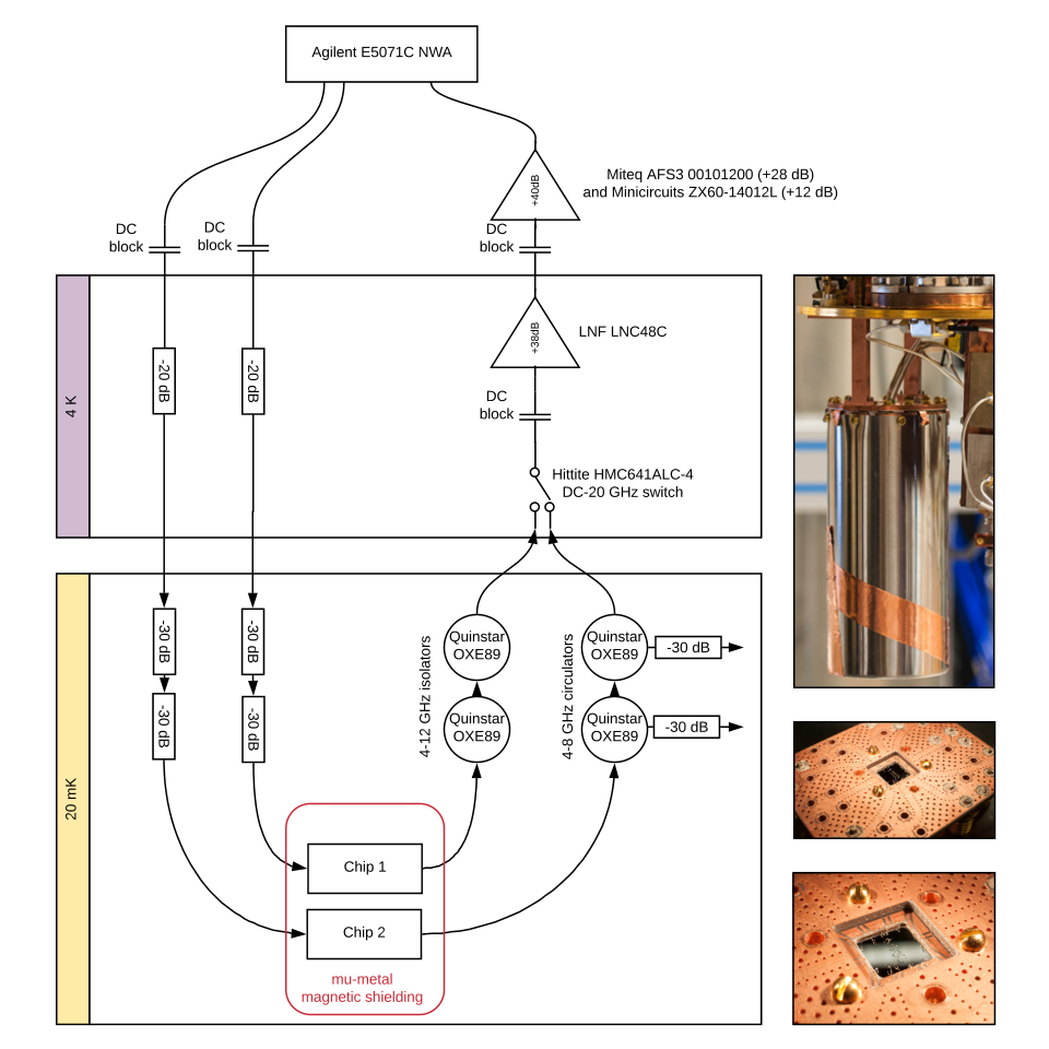
Each chip containing a series of resonators is mounted on a printed circuit board (See Fig. S3), which is mounted inside a can made of Mu-metal magnetic shielding. The can acts as another layer of radiation shielding and protects the resonators against stray magnetic fields. The PCB is bolted to the mixing chamber plate through a copper post to provide solid thermal anchoring.
Transmitted microwaves from the resonator pass through two wideband circulators or isolators (Quinstar OXE89) after which they are amplified by a cryogenic amplifier (LNF LNC48C). A final stage of amplification at room temperature, consisting of a Miteq AFS3-00101200 and a Minicrcuits ZX60-14012L, provides 28 dB and 12 dB of gain, respectively. The full transmission is measured using a Agilent E5071C network analyzer, which records both the transmitted amplitude and phase change.
Appendix E Film thickness uniformity across the wafer
To test for variations of film thickness across the wafer, we have measured resonance frequencies of two sets of identical resonators ( nm) from the same two inch diameter wafer. One of the chips was chosen from the center of the wafer, whereas the second was chosen closer to the edge. Their resonance frequencies were recorded and the result is shown in Fig. S4. The difference in resonance frequencies ranges from 5 to 50 MHz, which amounts to an average fractional difference . If this difference were entirely due to a non-uniform film thickness across the wafer, one would expect , where is the film thickness variation across the wafer. From this we estimate or nm.

Appendix F Temperature induced frequency shift
Figure S5a shows a quality factor decrease as function of temperature for four different film thicknesses. The solid lines in this figure are fits to a heuristic model that includes a temperature independent upper bound and its functional form is given by
| (F1) |
where
| (F2) |
is the superconducting gap at , and is the elliptic function of the first kind. Eq. (F2) is derived from the Mattis-Bardeen relations for the real and imaginary parts of the conductivity [36]. Bardeen-Cooper-Schrieffer theory predicts that depends on the critical temperature of the film through . A fit of the data to Eq. (F1) with only and as free parameters yields the solid lines in Fig. S5a.
Figure S5b shows extracted ’s from each of these fits as function of film thickness (diamond markers). These should be compared to the values obtained by four point resistance measurements from Table 1, which are visualized by gray bars. For each bar the height reflects the drop from the normal state resistivity (0.9 ) to zero resistance. We find that the fit consistently predicts higher ’s than measured by the four point resistance measurement. However, better agreement for the thickest films is obtained after rescaling with . The resulting ’s are shown as circles in Fig. S5b.
Besides the internal quality factor we also record the frequency shift as function of temperature. Theoretically, the frequency shift can be described by
| (F3) |
where , is the kinetic inductance fraction and is the imaginary part of the complex surface impedance, which is calculated by numerically integrating the Mattis-Bardeen equation for [37, 38, 39]. Figure S5c shows the measured frequency shift and prediction from BCS theory obtained by fitting the frequency shift to Eq. (F3). Most notably, the frequency shift of the 8.9 nm sample shows a clear deviation from the BCS prediction, whereas the thicker films fit better. Similar deviations from BCS theory have been observed for thin films of disordered TiN and NbTiN [22], and for NbN [40].
Another noteworthy feature of these data is a positive frequency shift for , as shown in the inset of the same figure. The magnitude of this frequency shift is only tens of kHz for the thinnest film and decreases with increasing film thickness. A possible candidate for this phenomenon could be two-level systems on the surface of the Si substrate or TiN [41, 42]. Under this assumption, the frequency shift can be written as
| (F4) |
Eq. (F4) predicts a positive frequency shift with temperature. Along with the observed power dependence of shown in Fig. 2b, these data strongly suggest the presence of two-level systems in our resonators. However, Eq. (F4) also predicts an initial decrease in , which we do not observe. The origin of the absence is not clear.

Appendix G High impedance resonator design
In this section, we derive expressions for and of the lumped element, high impedance resonators in Fig. 3a. The resonance frequency is given by , where , is the stray capacitance from the meandering wire to ground, and is the wire length. The resonator’s footprint can be approximated as a square with side length , such that , where is the effective dielectric constant. Therefore, the stray capacitance scales with the perimeter rather than the area for this resonator design. To estimate the scaling of with and , we note that the actual surface area of the inductor wire is . Therefore
| (G1) |
The scaling of the characteristic impedance with and comes from the relation . Plugging in Eq. (G1) yields
| (G2) |