Probing a spin transfer controlled magnetic nanowire with a single nitrogen-vacancy spin in bulk diamond
Abstract
The point-like nature and exquisite magnetic field sensitivity of the nitrogen vacancy (NV) center in diamond can provide information about the inner workings of magnetic nanocircuits in complement with traditional transport techniques. Here we use a single NV in bulk diamond to probe the stray field of a ferromagnetic nanowire controlled by spin transfer (ST) torques. We first report an unambiguous measurement of ST tuned, parametrically driven, large-amplitude magnetic oscillations. At the same time, we demonstrate that such magnetic oscillations alone can directly drive NV spin transitions, providing a potential new means of control. Finally, we use the NV as a local noise thermometer, observing strong ST damping of the stray field noise, consistent with magnetic cooling from room temperature to 150 K.
In nanoscale magnetic circuits, spin transfer (ST) effects provide an efficient means of all-electronic control, prompting the development of ST-based non-volatile memories, microwave-frequency oscillators, filters, detectors, and amplifiers [1, 2]. These developments call for new tools to understand the interplay between spins, magnons, and the environment. In parallel, the nitrogen-vacancy (NV) center in diamond [8] has emerged as a versatile sensor for studying magnetic systems, with excellent spatial and spectral resolution [4, 5]. The tiny magnetic moment of a single spin provides a non-invasive probe of local stray fields, and can be combined with scanned-probe [6] or subwavelength imaging [7] techniques to achieve nanoscale spatial resolution. Moreover, the NV offers a variety of sensing modalities appropriate for DC and AC magnetic fields [8, 9] or noise spectroscopy [10, 11, 12]. Recently, NV centers have probed ferromagnetic phenomena including vortex cores [13, 14], domain walls [15], ferromagnetic resonance (FMR) [16, 6, 18, 19, 26], and magnetic thermal quantities in an extended YIG film [26] modified by ST effects.
Here, we probe a metallic ST-controlled ferromagnetic nanowire with a single NV in bulk diamond. Different from microwave-frequency magnetoresistance readout [21, 22, 13], the NV’s point-like nature enables coupling to shorter-wavelength spin waves, thereby revealing qualitatively new features. First, we provide transport-based evidence of parametrically-driven magnetic oscillations – tuned through threshold with spin transfer anti-damping – and use the resulting (phase-locked) stray field oscillations alone to drive the NV spin resonance.


This demonstration removes any ambiguity from the interpretation of the transport measurements, and provides a potential new means of NV control. Additionally, transport readout indicates a precession angle up to 55∘, suggesting the absence of Suhl-like (multi-magnon) instabilities [24], which we tentatively attribute to the reduced density of states in our confined geometry. The observed changes in field at the NV independently corroborate the estimated angle, and (more importantly) we observe no signs of NV spin flips in the PL spectra when directly driving FMR – a feature normally appearing in extended magnetic films [16, 6, 18, 19, 26] – providing additional evidence of suppressed multi-magnon instabilities. This highlights the NV’s potential use as a tool for understanding internal workings of magnetic nanosystems. Finally, we demonstrate strong ST control of the magnetic thermal fluctuations: adapting the NV noise relaxometry method of Ref. [26], we observe large ST damping of the stray field noise, providing evidence of magnetic cooling from room temperature to 150 K. The observed noise suppression is orders of magnitude larger than measured with an NV near a YIG film [26], and a factor of 2 larger than measured with Brillouin light scattering from a related metallic structure [25]. An interesting open question is the fundamental limits of this cooling technique, in particular if and from what temperature the ground state can be reached. Interestingly, our demonstrated NV sensitivity suggests it may be possible to resolve magnetic zero-point fluctuations, thereby providing an optically active “handle” on a macroscopic magnet in the quantum regime.
These techniques, which are especially advantageous in systems having low magnetoresistance, pave the way to a deeper understanding of short-wavelength magnons, ST effects, and quantum emitter control.
I Device Geometry
We fabricate [26] an -m-long -nm-wide Py (, 10 nm) / Pt (10 nm) multilayer nanowire on electronic grade diamond with a layer of NVs implanted nm below the surface, as shown in Fig. 1(a). Figure 1(b) shows a photoluminescence (PL) image of the device pumped (532 nm) and collected (594 nm) from above. Bright spots are NVs, the nanowire appears dark, and the contacts (Au) exhibit typical background PL. We focus on the indicated spot, with PL primarily from single NV whose symmetry axis lies from the -axis in the plane [26]. Static magnetic fields are applied with a permanent neodymium magnet on a motorized stage, calibrated using the NV spin transitions [26]. For this device, a moderate field ( mT) applied along the NV symmetry axis saturates the Py magnetization along , canted at most 3∘ out of the plane (dictated by shape anisotropy [26]). All measurements are taken at room temperature.

II Transport Characterization of Magnetic Resonances
To verify the device’s functionality, we perform ferromagnetic resonance (FMR) by applying current through the nanowire (bias , amplitude , frequency ), and reading the anisotropic magnetoresistance (AMR) response via a generated DC voltage [11, 26]. Due to the spin Hall effect, the electrical current drives a pure spin current (polarized along ) into the Py layer, applying a torque on the Py magnetization’s unit vector . The field generated by this current applies a torque along .
A “typical” ST-FMR spectrum for field mT applied along the NV axis but rotated about is shown in Fig. 2(a) (blue circles), with , and mA. The resonant feature at 1.6 GHz is well fit by the expected Fano-like lineshape [11, 26], allowing us to extract the resonant frequency and linewidth . Figure 2(b) shows the field dependence of these spectra (color scale) and the fit values of (points). The initial decrease in frequency corresponds to the equilibrium orientation shifting from (where shape anisotropy provides GHz) and saturating along , where the anisotropy field opposes the applied field. When (Fig. 2(a), orange squares), this FMR signal vanishes (as expected above the saturation field), since both the drive torques and AMR response also vanish to lowest order in and [26]. Figure 2(c) shows the field dependence of these spectra, along with estimated from values at [26]. Above saturation, is well fit by the Kittel formula for spatially uniform , providing effective in-plane (out-of-plane) coercive fields mT ( mT) [26].
Figure 2(d) shows the same measurement with mA. This applies a steady torque along that anti-damps the magnetization ( also shifts saturation to higher fields). Importantly, a significantly larger, asymmetric peak appears near twice the expected FMR frequency (see Fig. 2(a), red symbols), suggesting parametrically driven, large-amplitude oscillations. Simple macrospin simulations [26] reproduce the sign, magnitude, frequency, and line shape of this feature semi-quantitatively, and we interpret it as arising from a large-angle elliptical precession [21] of the spatially-averaged magnetization. Within this macrospin approximation, the largest-amplitude signal (120 V) in Fig. 2(a) corresponds to an in-plane (out-of-plane) precession angle (6∘).
III NV Response to Parametric Oscillations
This picture is validated by the NV’s PL spectrum shown in Fig. 3. First, while driving the nanowire at frequency , we apply a -pulse with a nearby stripline to determine the NV’s lower electron spin resonance (ESR) frequency. Figure 3(a) shows the PL response (top) and (bottom) for field mT along the NV axis. Reductions in PL are associated with driving the NV spin from its spin projection to , occurring at resonant frequencies . Notably, the frequency of the stripline-driven transition shifts by up to 13 MHz when is driven to large amplitude, and follows a path qualitatively similar to . The maximum shift in corresponds to a decrease in the NV-axial magnetic field of 0.5 mT, as expected for the reduced average magnetization. This is a large fraction of the estimated 2.4 mT total stray field [26], corresponding to an in-plane precession angle that is within of the value (55∘) estimated from in Fig. 3(a).
More compellingly, we can drive the NV transition using only the Py layer’s stray field. Figure 3(b) shows a similar set of measurements in the absence of stripline current, with tuned to 29.6 mT, such that . Above mA, a PL dip (corresponding to field-driven transitions) appears at twice , as expected for parametric oscillations at half the drive frequency. Figure 3(c) shows the contrast and linewidth of this PL dip for a wider bias range, illustrating a sharp threshold at mA. This measured PL response provides unambiguous evidence of ST anti-damping and large-amplitude, parametrically driven oscillations. We note that details such as the precise threshold current and shapes of the bias dependences in (c), depend somewhat on , which slightly tunes the NV and FMR frequencies.

In Fig. 4, we map out the parametrically driven phase space of (a) , and (b) PL under the same conditions as Fig. 3. For this larger drive, new features appear above the primary parametric peak, which we tentatively attribute to higher order spin-wave modes [14]. Of interest, the Py-driven PL feature near from Fig. 3(b) extends over a wide range of fields, consistent with the presence of these higher-frequency transport features.
At this larger drive, we observe a residual directly-driven precession amplitude up to at in the transport data (Fig. 4(a)). Despite this, we observe no evidence of spin flips at in the PL spectra of Fig. 4(b), contrasting what is ubiquitously observed near extended films [16, 6, 18, 19, 26]. We tentatively attribute this to the reduced density of states in our confined geometry, which acts to suppress multi-magnon up-conversion processes.
Finally, as shown in the inset, the Py-driven spin resonance splits by up to 60 MHz at some fields. The nature of this splitting will be the subject of future work, but we suspect it is due to the presence of quasistable magnetic modes [30, 31] having different average stray fields. Notably, information about these dynamics are not apparent in (a), highlighting this technique’s potential to provide qualitatively new information.
IV Strongly Damped Magnetization
The associated NV spin relaxation rates can also probe the local field noise, providing some information about the thermal occupancy of spin wave modes [26, 25]. Stated briefly, the noise spectral density of the stray field perpendicular to the NV axis (units of T2/Hz) should have the form
| (1) |
where is the thermal occupancy of the spin wave mode having wavenumber and frequency , is a constant converting magnon number to field noise power, and is a density function describing how this power is spread over the frequency domain (peaked at ). In the presence of , the NV spin relaxation rate increases from its nominal value Hz [26] to a value
| (2) |
where is the gyromagnetic ratio of the NV spin. Figure 5(a) shows the measured [26] relaxation rates for varied field , along with and below. Qualitatively similarly to extended YIG films [26], the largest relaxation occurs when when is just above , with peak value determined by the balance of , , (which takes the largest value when is comparable to the NV-wire distance), and the density of spin wave states. In contrast to Ref. [26], spin-transfer damping (and antidamping) in this confined metallic system should completely dominate over Joule heating (the nanowire temperature changes at most by 5 K [26]), enabling strong modification of the thermal fluctuations. Figure 5(b) shows how varies with (while simultaneously compensating to fix ); the weaker -generated field at the NV leads to modest shifts of in Fig. 5(d). Both relaxation rates significantly decrease for negative current (damping), indicating a strong suppression of stray field noise, and increase for positive current (antidamping). Naively assuming these changes arise entirely from , and that the action of damping is to modify the effective magnetic temperature [25, 26], the observed change in corresponds to ST cooling to K at mA. However, the probe frequencies drift with and the ST damping broadens the peak in . A model combining these effects with the observed field-dependence in Fig. 5(a) [26] produces the “spin transfer free” relaxation rate estimates shown in Fig. 5(b) and the color scale in the lower panels of (a) and (b). Importantly, the expected changes are much smaller (and have the opposite trend), suggesting that our estimate of might represent an upper bound. We note that, in this geometry, we could not extract trustworthy parameters from FMR at maximum damping, highlighting the utility of the NV as an independent probe.
V Conclusions
The NV PL spectrum provides qualitatively different information about magnetic nanocircuits than is provided by traditional transport measurements. We demonstrated parametric magnetic oscillations controlled by ST effects, and that ESR transitions can be driven entirely by a local magnetization. The latter technique may potentially facilitate fast, low-power control of NV spins, and the nonlinear dynamics involved could, e.g., be used to amplify incident fields [14]. We also observe large changes in the NV spin relaxation time when subjecting the magnetic element to ST damping, consistent with magnon cooling to well below ambient temperatures. Finally, we note that the demonstrated stray field coupling between the NV and spin wave modes is quite large. Of note, Fig. 5(a) exhibits a maximal at 15.5 mT, where corresponds to a room-temperature magnon occupancy 2500, meaning the noise generated by the ferromagnetic zero-point fluctuations would set 1 Hz. This value is comparable to the intrinsic relaxation rates of bulk NV’s at low temperature [32], suggesting it might be feasible to resolve the quantum fluctuations of a magnetic nanocircuit.

VI Acknowledgments
We thank Luke Hacquebard, Quentin Pognan, Isabelle Racicot, Souvik Biswas, and Tsvetelin Totev for discussions and related work. JS, LC, and M-PL acknowledge support from Fonds de Recherche - Nature et Technologies (FRQNT) PR-181274. LC acknowledges funding support from Canada Foundation for Innovation and Canada Research Chairs (CRC) project 229003, National Sciences and Engineering Research Council of Canada (NSERC) RGPIN 435554-13, and l’Institut Transdisciplinaire d’Information Quantique (INTRIQ). JS acknowledges support from CRC project 228130 & 231509. LC and JS acknowledge Benjamin Childress and Calvin Childress for all sleep-deprived errors in judgment, including this acknowledgment.
References
- [1] D. Ralph and M. Stiles, “Spin transfer torques,” J. Mag. & Mag. Mat. 320, 1190 (2008).
- [2] A. Manchon, I. M. Miron, T. Jungwirth, J. Sinova, J. Zelezný, A. Thiaville, K. Garello, and P. Gambardella, “Current-induced spin-orbit torques in ferromagnetic and antiferromagnetic systems,” arXiv:1801.09636 (2018).
- [3] M. W. Doherty, N. B. Manson, P. Delaney, F. Jelezko, J. Wrachtrup, and L. C. Hollenberg, “The nitrogen-vacancy colour centre in diamond,” Phys. Rep. 528, 1 (2013).
- [4] L. Rondin, J.-P. Tetienne, T. Hingant, J.-F. Roch, P. Maletinsky, and V. Jacques, “Magnetometry with nitrogen-vacancy defects in diamond,” Rep. Prog. in Phys. 77, 056503 (2014).
- [5] F. Casola, T. van der Sar, and A. Yacoby, “Probing condensed matter physics with magnetometry based on nitrogen-vacancy centres in diamond,” Nature Rev. Mat. 3, 17088 (2018).
- [6] P. Maletinsky, S. Hong, M. S. Grinolds, B. Hausmann, M. D. Lukin, R. L. Walsworth, M. Loncar, and A. Yacoby, “A robust scanning diamond sensor for nanoscale imaging with single nitrogen-vacancy centres,” Nature Nano. 7, 320 (2012).
- [7] E. Rittweger, K. Han, S. Irvine, C. Eggeling, and S. W. Hell, “STED microscopy reveals crystal colour centres with nanometric resolution,” Nature Phot. 3, 144 (2009).
- [8] C. L. Degen, “Scanning magnetic field microscope with a diamond single-spin sensor,” Appl. Phys. Lett. 92, 243111 (2008).
- [9] J. M. Taylor, P. Cappellaro, L. Childress, L. Jiang, D. Budker, P. R. Hemmer, A. Yacoby, R. Walsworth, and M. D. Lukin, “High-sensitivity diamond magnetometer with nanoscale resolution,” Nature Phys. 4, 810 (2008).
- [10] J.-P. Tetienne, T. Hingant, L. Rondin, A. Cavaillès, L. Mayer, G. Dantelle, T. Gacoin, J. Wrachtrup, J.-F. Roch, and V. Jacques, “Spin relaxometry of single nitrogen-vacancy defects in diamond nanocrystals for magnetic noise sensing,” Phys. Rev. B 87 (2013a).
- [11] T. Rosskopf, A. Dussaux, K. Ohashi, M. Loretz, R. Schirhagl, H. Watanabe, S. Shikata, K. M. Itoh, and C. L. Degen, “Investigation of surface magnetic noise by shallow spins in diamond,” Phys. Rev. Lett. 112, 147602 (2014).
- [12] B. A. Myers, A. Das, M. C. Dartiailh, K. Ohno, D. D. Awschalom, and A. C. Bleszynski Jayich, “Probing surface noise with depth-calibrated spins in diamond,” Phys. Rev. Lett. 113, 027602 (2014).
- [13] J.-P. Tetienne, T. Hingant, L. Rondin, S. Rohart, A. Thiaville, J.-F. Roch, and V. Jacques, “Quantitative stray field imaging of a magnetic vortex core,” Phys. Rev. B 88, 214408 (2013b).
- [14] R. Badea, M. S. Wolf, and J. Berezovsky, “Exploiting bistable pinning of a ferromagnetic vortex for nitrogen-vacancy spin control,” Appl. Phys. Lett. 109, 132403 (2016).
- [15] J.-P. Tetienne, T. Hingant, J.-V. Kim, L. H. Diez, J.-P. Adam, K. Garcia, J.-F. Roch, S. Rohart, A. Thiaville, D. Ravelosona, and V. Jacques, “Nanoscale imaging and control of domain-wall hopping with a nitrogen-vacancy center microscope,” Science 344, 1366 (2014).
- [16] C. S. Wolfe, V. P. Bhallamudi, H. L. Wang, C. H. Du, S. Manuilov, R. M. Teeling-Smith, A. J. Berger, R. Adur, F. Y. Yang, and P. C. Hammel, “Off-resonant manipulation of spins in diamond via precessing magnetization of a proximal ferromagnet,” Phys. Rev. B 89, 180406 (2014).
- [17] T. van der Sar, F. Casola, R. Walsworth, and A. Yacoby, “Nanometre-scale probing of spin waves using single electron spins,” Nature Comm. 6, 7886 (2015).
- [18] C. S. Wolfe, S. A. Manuilov, C. M. Purser, R. Teeling-Smith, C. Dubs, P. C. Hammel, and V. P. Bhallamudi, “Spatially resolved detection of complex ferromagnetic dynamics using optically detected nitrogen-vacancy spins,” Appl. Phys. Lett. 108, 232409 (2016).
- [19] M. R. Page, F. Guo, C. M. Purser, J. G. Schulze, T. M. Nakatani, C. S. Wolfe, J. R. Childress, P. C. Hammel, G. D. Fuchs, and V. P. Bhallamudi, “Optically Detected Ferromagnetic Resonance in Metallic Ferromagnets via Nitrogen Vacancy Centers in Diamond,” arXiv:1607.07485 (2016).
- [20] C. Du, T. van der Sar, T. X. Zhou, P. Upadhyaya, F. Casola, H. Zhang, M. C. Onbasli, C. A. Ross, R. L. Walsworth, Y. Tserkovnyak, and A. Yacoby, “Control and local measurement of the spin chemical potential in a magnetic insulator,” Science 357, 195 (2017).
- [21] S. I. Kiselev, J. C. Sankey, I. N. Krivorotov, N. C. Emley, R. J. Schoelkopf, R. A. Buhrman, and D. C. Ralph, “Microwave oscillations of a nanomagnet driven by a spin-polarized current,” Nature 425, 380 (2003).
- [22] A. A. Tulapurkar, Y. Suzuki, A. Fukushima, H. Kubota, H. Maehara, K. Tsunekawa, D. D. Djayaprawira, N. Watanabe, and S. Yuasa, “Spin-torque diode effect in magnetic tunnel junctions,” Nature 438, 339 (2005).
- [23] J. C. Sankey, P. M. Braganca, A. G. F. Garcia, I. N. Krivorotov, R. A. Buhrman, and D. C. Ralph, “Spin-transfer-driven ferromagnetic resonance of individual nanomagnets,” Phys. Rev. Lett. 96 (2006).
- [24] H. Suhl, “The theory of ferromagnetic resonance at high signal powers,” J. Phys. & Chem. Solids 1, 209 (1957).
- [25] V. E. Demidov, S. Urazhdin, B. Divinskiy, V. D. Bessonov, A. B. Rinkevich, V. V. Ustinov, and S. O. Demokritov, “Chemical potential of quasi-equilibrium magnon gas driven by pure spin current,” Nature Comm. 8 (2017).
- [26] See supplementary materials for more information.
- [27] L. Liu, T. Moriyama, D. C. Ralph, and R. A. Buhrman, “Spin-torque ferromagnetic resonance induced by the spin Hall effect.” Phys. Rev. Lett. 106, 036601 (2011).
- [28] A. Dreau, M. Lesik, L. Rondin, P. Spinicelli, O. Arcizet, J.-F. Roch, and V. Jacques, “Avoiding power broadening in optically detected magnetic resonance of single NV defects for enhanced dc magnetic field sensitivity,” Phys. Rev. B 84, 195204 (2011).
- [29] Z. Duan, C. T. Boone, X. Cheng, I. N. Krivorotov, N. Reckers, S. Stienen, M. Farle, and J. Lindner, “Spin-wave modes in permalloy/platinum wires and tuning of the mode damping by spin Hall current,” Phys. Rev. B 90 (2014).
- [30] J. Sankey, I. Krivorotov, S. Kiselev, P. Braganca, N. Emley, R. Buhrman, and D. Ralph, “Mechanisms limiting the coherence time of spontaneous magnetic oscillations driven by dc spin-polarized currents,” Phys. Rev. B 72 (2005).
- [31] D. V. Berkov and N. L. Gorn, “Magnetization oscillations induced by a spin-polarized current in a point-contact geometry: Mode hopping and nonlinear damping effects,” Phys. Rev. B 76 (2007).
- [32] A. Jarmola, V. M. Acosta, K. Jensen, S. Chemerisov, and D. Budker, “Temperature- and magnetic-field-dependent longitudinal spin relaxation in nitrogen-vacancy ensembles in diamond,” Phys. Rev. Lett. 108 (2012).
- [33] C. Lee, E. Gu, M. Dawson, I. Friel, and G. Scarsbrook, “Etching and micro-optics fabrication in diamond using chlorine-based inductively-coupled plasma,” Diamond & Rel. Mat. 17, 1292 (2008).
- [34] Y. Chu, N. de Leon, B. Shields, B. Hausmann, R. Evans, E. Togan, M. J. Burek, M. Markham, A. Stacey, A. Zibrov, A. Yacoby, D. Twitchen, M. Loncar, H. Park, P. Maletinsky, and M. Lukin, “Coherent optical transitions in implanted nitrogen vacancy centers,” Nano Lett. 14, 1982 (2014).
Supplementary Information
1 Device fabrication
We fabricate an 8-m-long 417-nm-wide Py () / Pt nanowire (layer thicknesses nm and nm) on CVD-grown, electronic grade diamond (Element Six), as shown in Fig. 1 of the main text. Prior to depositing the nanowire, we relieve strain and smooth the diamond surface to 0.2 nm-rms over micron length scales (0.05 nm-rms over smaller scales) with Ar/Cl2 etching [1], then create a layer of NV centers 7515 nm below the surface with 15N+ implantation (60 keV, Innovion Corp.) and high-temperature annealing [2]. A subsequent Ar/O2 plasma etch (20 mTorr, 35 sccm Ar, 10 sccm O2, 108 W RF for 45 sec; etches 20 nm/min) removes contaminants and reduces the NV depth to 6015 nm. To remove any residual graphitized carbon and oxygen-terminate the surface, we perform a final clean in a boiling 1:1:1 mixture of nitric, perchloric, and sulfuric acid at 200∘ C for 1 hour. The Py/Pt nanowire is deposited with e-beam lithography, sputtering, and liftoff (we recommend a more directional deposition, e.g., evaporation to improve liftoff yield). We then deposit Ti (10 nm) / Au (50 nm) macroscopic leads and a microwave stripline (10 m wide, 17 m center-to-center distance) using photolithography, and finally connect the leads to the nanowire with another e-beam liftoff (Ti (10 nm) / Au (70 nm) evaporated). The contacts leave an “active” region of length m exposed.
2 NV measurements
2.1 Single NV identification and isolation
We focus on an NV center (“NVA”) having the strongest stray field coupling. However, this NV is positioned near a second NV “NVB”, that provides an additional small photoluminescence (PL) signal. As described below, we identify these two NVs using a combination of electron spin resonance (ESR) spectroscopy and photon correlation measurements, taking advantage of their different symmetry axes to isolate signals from NVA.
The two NVs are both associated with the single bright emission spot shown in Fig. 1(b) of the main text. With the 532 nm excitation focused on this spot, we observe ESR spectra indicating the presence of NVs having two different orientations. Figure 1 shows two ESR spectra taken with a 6 mT magnetic field oriented 35∘ from the diamond surface in the and planes, such that it is aligned with one of the allowed 111 crystallographic orientations of the diamond bonds (i.e., along one of the allowed NV symmetry axes). Dips in PL are associated with driving the NV from its spin projection to , occurring at frequencies (nominally GHz at zero field). The deepest photoluminescence dip in both spectra is associated with transition of the better-coupled NV center (NVA), mostly because the polarization of the 532 nm excitation is perpendicular to the NVA symmetry axis. This transition shows the largest magnetic field dependence when the field is in the plane, parallel to NVA (corresponding to the arrow in Fig. 1(a) of the main text), while the shallower transition of NVB shows the largest deviation with the field aligned in the plane. Note that the transition of NVA is barely visible above the noise in each spectrum, due to imperfect power coupling to our stripline at the higher frequencies (this is also why we do not see the transition for NVB in these spectra). In principle, there could be multiple NVs creating the observed spectra, but the total photon count rate is approximately what we expect for two NVs. Moreover, because the emission spot is close to the magnetic nanowire, in a region of high magnetic field gradient, NVs with the same orientation would be expected to show distinct ESR lines. We see no evidence of unexpected dips under any conditions, lending additional credence to the identification of two NVs.
To further verify our interpretation that only two NV centers are co-located within the emission spot, we perform photon correlation measurements to estimate the number of contributing emitters. The second order correlation function was measured with a Hanbury-Brown-Twiss setup, using a fiber beam-splitter and two single photon counting modules. A time-correlated single photon counting system (PicoHarp 300) was used to measure the histogram of times between two consecutive photons. Such a normalized distribution can be interpreted as a measurement of , as long as is much smaller than the mean time between two detection events (for us, 1/count rate= kcounts/s 33 s) [3]. We measure a background count rate (on a dark area of the sample) of 3 kcounts/s, which we subtract from our data before analysis.
Our data shows a clear anti-bunching signature at short times (see Fig. 2), characteristic of a small number of quantum emitters, and slight bunching at longer times, associated with metastable states in the emitters. To quantify requires that we appropriately normalize the data. Merely setting the long-time value to 1 is problematic because of the exponential decay associated with the fact that we are not directly measuring the correlation function but a histogram of times between photons. Indeed, we observed such an exponential decays for measured with attenuated laser light. We thus compensate for the decay by fitting an exponential with a decay constant , to the data from 1 s onward. Multiplying the full spectrum of data points by corrects for the exponential decay, and allows us to used the long-time value for our normalization. We then use a three level model to fit the curve to the function [4]:
| (1) |
where c1,2,3 are scaling factors and correspond to the lifetimes of the involved NV states. We find that 0.01, consistent with two co-located emitters, where one is slightly better coupled to our optical excitation/collection path than the other.
In our measurements, we isolate NVA from NVB by taking advantage of their different orientations. For ESR measurements (such as in Fig. 3 of the main text), the transitions of NVA and NVB are spectrally resolved. Moreover, we align the polarization of the 532 nm illumination to preferentially excite NVA, reducing photoluminescence from NVB; we also work in magnetic fields aligned with NVA, which reduces the ESR contrast of NVB. As a result, the resonances from NVB are only weakly visible in the spin resonance data shown in Fig. 4(b) of the main text. For spin relaxation measurements, we use pulses tuned to the transitions of NVA to isolate its relaxation rates from those of NVB, as described in further detail below.
2.2 Extracting spin relaxation rates
We extract the two relaxation rates for NVA by initializing the spin into the three spin projections , observing its relaxation via photoluminescence measurements, and fitting our data to a rate equation model.
We prepare the spin projections using a pulse of 532 nm excitation, which optically pumps both NVA and NVB into ; to prepare , we then apply a pulse of microwaves tuned to the NVA spin transitions for durations of 50-200 ns, chosen to maximize the contrast of a Rabi sequence. These pulses are far off resonance with NVB, so it remains in . After a variable delay of duration , we again apply a pulse of 532 nm excitation and observe photoluminescence counts, which are higher for states than for . In the end, we record three photoluminescence traces: , and , where the subscript indicates the spin state into which NVA was initialized.
Since these photoluminescence traces include emission from both NVA and NVB, we consider the differences in the photoluminescence traces and . Because NVB is prepared in the same way for all three initializations, its (possibly -dependent) photoluminescence is eliminated in the data sets , as is any background photoluminescence not associated with NVA.
We then simultaneously fit and to a rate equation model for spin relaxation:
| (2) |
where is the population of NVA in spin state and are the relaxation rates on the transitions. We also considered double quantum relaxation between states, but our fits revealed that this rate was insignificant. The fit functions for are found by calculating the population in for three different spin initializations, (where the superscript indicates the initial state), and subtracting to reconstruct a signal proportional to . Note that this proportionality holds even for imperfect optical pumping and imperfect pulses – low fidelity initialization and incomplete pulses reduce the contrast of our signals, but not their time dependence. We can thus fit to , where is an unknown fitting parameter, and extract the two relaxation rates .
3 Magnetic field calibration
We apply static magnetic fields using a permanent magnet (K&J magnetics, D42-N52) mounted on a three-axis translation stage equipped with closed-loop motorized actuators (CONEX-TRB25CC). The 25mm range of motion permits us to apply magnetic fields up to 90 mT oriented along the NV symmetry axis.
To calibrate the relationship between the actuator position and the applied magnetic field, we exploit the field-dependent photoluminescence of the NV center [5]. Essentially, NV photoluminescence is maximized when the magnetic field is parallel to its symmetry axis, with heightened sensitivity near the ground- and excited-state level anti-crossings near 103 mT and 51 mT, respectively. Following the procedure described in Ref. [6], we measure the photoluminescence of an NV as a function of the position of the permanent magnet. From this data, we can extract the controller coordinates that bring the NV center to the excited state level anti-crossing (51 mT) and align the magnetic field with the NV axis. We then model the stray field of the permanent magnet using RADIA [7] and determine the position (relative to the permanent magnet origin) where the stray field is 51 mT aligned with the NV axis. This provides a coordinate transformation between our controller position and the model. We can then use the RADIA model to roughly predict the field as a function of controller position. We design a trajectory for the magnet that should maintain the magnetic field along the NV axis or at a defined angle relative to that axis.
This calibration procedure gives only an approximation of the magnetic field due to potential inaccuracy of the RADIA model and possible misalignment between the (nominally aligned) coordinate axes of our sample and the controller axes. We therefore use NV electron spin resonance (ESR) measurements to determine the actual magnetic field taken along the trajectories used in our experiments. Note that these measurements were taken after the device magnetization disappeared (see Sec. 6.4.1), so the NV experiences only the applied magnetic field. We fit the ESR spectra to extract the transition frequencies . From the linear and quadratic Zeeman effects, we can determine the on- and off-axis components of the magnetic field [6], and thus calculate its magnitude. Figure 3(a) shows the difference between the extracted and expected field magnitudes as a function of the expected field predicted by the RADIA model. These values are found using an NV g-factor of 2.0030(3) and a zero field splitting of 2.870(2) GHz, consistent with our observed splittings and literature values [8, 9]. The solid red curve is a sixth order polynomial interpolating function used to rescale the magnitudes of the magnetic fields in the data presented in the main text. Figure 3(b) shows the extracted angle of the magnetic field, which is poorly constrained by these measurements; due to the good ESR contrast observed over the entire magnetic field scan at in Fig. 4(b) of the main text, and the strong suppression of directly-driven FMR at , we believe the angular alignment is good to within a couple of degrees.
4 Spin transfer control and magnetoresistive readout
We control the magnetization of the Py layer with current in the nanowire, which provides two torques. First, as indicated in Fig. 1(a) of the main text, the current density in the Pt layer produces a spin current density (where is Pt’s spin Hall angle), polarized along and travelling along [10]. A fraction of these spins are absorbed by the Py layer ( [11]), thereby applying an areal spin transfer torque (STT) density at the Py interface, or an effective per-volume torque density (Nm/m3)
| (3) |
where the unit vector represents the orientation of the local magnetization. Second, the current in the wire generates a magnetic field in the Py layer, with a torque (volume) density
| (4) |
where is the Py saturation magnetization. Changes in the magnetization can then be read out via the device’s resistance, which varies approximately11 1 This assumes , which is justified by the calculations and simulations in Sec. 6. as
| (5) |
where is the wire’s unbiased resistance at , and m is the change due to anisotropic magnetoresistance (AMR) from the fraction of current flowing through the Py layer (measured by monitoring while sweeping the field).
To verify device functionality, we perform spin transfer ferromagnetic resonance (ST-FMR) similar to that of Ref. [11]. To briefly summarize, a current (with DC bias , “radio frequency” (RF) amplitude , and frequency ) driving coherent resistance oscillations (for constant offset , amplitude , and phase ) will generate a time-averaged voltage change
| (6) |
that can be read out with a lock-in technique (see Sec. 5.2). This voltage comprises a resonant magnetoresistance signal (estimated for a macrospin in Sec. 6) and a broad background due to Joule heating (useful for estimating , as discussed in Sec. 5) that is subtracted from all presented spectra.
5 Joule heating background, differential resistance, and RF current calibration
When a time-dependent current passes through a resistive wire, it dissipates a time-dependent power, thereby heating the sample and causing a time-dependent change in resistance. In general, this nonlinear response can generate a static voltage across the resistor. Here we develop a framework for quantifying this effect, and show how it can be used to provide a reasonable estimate of the RF current flowing through our nanowires. This calibration considers RF temperature oscillations not included in (e.g.) Tshitoyan et al [12], which are especially relevant when the substrate is highly thermally conductive.
5.1 Derivation of Joule heating mixdown voltage
In general, the instantaneous voltage will depend on current and the change in temperature . For small and , we can Taylor expand to 3rd order:
| (7) | ||||
| (8) | ||||
| (9) |
where all of the parenthetical factors are constants of the system determined by the resistor’s geometry, materials, and thermal anchoring. We simplify this with the following assumptions:
- 1.
In the absence of temperature change, the resistor responds linearly. This means the terms (red) having no temperature dependence ; as a result, as well.
- 2.
Changing the temperature does not on its own generate a voltage. This means the current-independent terms (teal).
- 3.
The temperature change to lowest order, meaning the penultimate term (blue) is of order and can be dropped.22 2 In systems having a more significant Peltier effect (e.g., some spin valves), this should not be dropped.
Under these assumptions,
| (10) |
The first term is the heat-free linear response of the resistor, with the constant being the resistance near . We emphasize that is a constant that does not depend on or (all differentials in Eq. 10 are evaluated at ) and is qualitatively different from laboratory measurements commonly referred to as “differential resistance”, wherein the current is slowly modulated and the resulting voltage modulations are recorded (see Section 5.2).
The second term is the Joule heating nonlinearity of interest; an “extra” voltage can be generated from this term only if there is both a current and a temperature change. For example, if is some constant value, this will heat the sample, causing , which raises the resistance by , at which point produces an additional voltage. If changes slowly enough with time that the system remains in steady state, it is this term that is responsible for a bias dependence in a low-frequency differential resistance measurement (see Sec. 5.2.1).
We eliminate temperature by assuming small enough changes that responds linearly to the applied power . In this limit, an oscillatory component in the power of amplitude and frequency will induce a temperature change
| (11) |
where and (units of K/W) represent the thermal transfer function of the wire, capturing the magnitude and phase shift of the thermal response.33 3 We choose this quadrature formulation of the transfer function over the “usual” complex one due to the nonlinear operations in the rest of the analysis. The quadrature basis is also very convenient for calculating the mixdown voltage, which requires only the in-phase component . In our experiments, we apply a current of the form
| (12) |
for constants , and frequency , such that the instantaneous power is, to leading order (again assuming negligible Peltier effects)
| (13) |
This comprises a thermal drive at three frequencies (zero, , and ) which, in this linear-response limit, can be treated separately. As such, the temperature
| (14) |
with
| (15) | ||||
| (16) | ||||
| (17) |
Plugging Eq. 14 into the voltage expansion of Eq. 10,
| (18) | ||||
| (19) | ||||
| (20) | ||||
| (21) |
Taking a time-average yields
| (22) |
where we have defined a fractional resistance change transfer function
| (23) |
for brevity (units of 1/mA2). The first term is Ohm’s law and the second is the steady state heating due to DC current. The third term is the response to an RF drive, and is responsible for large backgrounds observed in FMR (see Sec. 5.2.2). Importantly, this comprises two terms, the first arising from the time-averaged power absorbed by the wire, and the second ( arising from the heat-induced resistance oscillations at mixing with the drive current.
5.2 Differential resistance and estimation of RF current
We now discuss a means of interpreting the signal from a lock-in-based differential resistance measurement in the presence of DC and RF current. Section 5.2.1 discusses a “traditional” continuous-wave lock-in approach, and Sec. 5.2.2 discusses an impulse method that happens to be easier with our apparatus. Section 5.2.4 then discusses a means of using the observed voltages in these measurements to estimate the RF current flowing through the device.
5.2.1 Traditional lock-in readout
When “differential resistance” is measured using a lock-in technique, the bias is modulated, such that the current
| (24) |
where is the lock-in’s modulation amplitude, and is the modulation frequency (typically chosen to be low enough that the device remains in steady state). In this case, the voltage (Eq. 22) becomes
| (25) | ||||
| (26) |
where we have lumped all terms not contributing to the measured amplitude at into “…” for brevity, and used the identity
| (27) |
The lock-in measurement demodulates at to record the response amplitude, which is then divided by to define a “differential resistance”
| (28) |
Note this result agrees with Eq. 22 in the low-frequency limit , but here we can see how the presence of RF current will alter this signal.
5.2.2 Impulse readout
In our experiment, we employ an impulse readout of wherein the amplitude of the modulation is slowly increased to its maximum value and then decreased to zero as
| (29) | ||||
| (30) | ||||
| (31) |
where is a large integer. We have expanded in the last line to highlight that this waveform includes only 3 frequencies near , which helps minimize artifacts associated with abrupt changes in current. Similar to the continuous-wave measurement, the device responds adiabatically for sufficiently small , and the low-frequency voltage becomes
| (32) | ||||
| (33) |
where “DC” contains all time-independent terms. We then extract a similar “differential resistance” by taking an overlap with the injected impulse to extract a (normalized) “in-phase” response amplitude
| (34) | ||||
| (35) |
By symmetry, the even powers of in Eq. 33 vanish, leaving behind
| (36) |
In practice, the measured value of does not depend on frequency below Hz (limited in our case by the low-pass action of our bias-T), which allows us to estimate from the bias-dependence of in the absence of RF current (). Figure 4 shows a measurement of , with 265 Hz. The data is well-fit by Eq. 36 (with a small offset bias A), from which we extract , mA-2. The small offset current is likely due to a combination of non-ideal electronics and Peltier effects associated with asymmetric contacts to our nanowire on chip. In the present experiment, this offset leads to at most a few-percent error in our calibration of (discussed below), along with a small, smoothly-varying background signal in our ferromagnetic resonance measurements of up to 5 V at low frequencies. The associated correction, which does not affect the central conclusions of the present work, will be the subject future work.
5.2.3 Maximum change in wire temperature
In the presence of only DC bias, Eq. 22 simplifies to
| (37) |
such that the DC resistance
| (38) | ||||
| (39) |
where is the temperature coefficient of resistance. From this, we identify
| (40) | ||||
| (41) |
Using the above fit values and using the Pt coefficient K as a lower bound, we place an upper bound on the maximum Joule heating temperature change K for our bias range ( mA).
5.2.4 Estimating RF current from rectified voltage
Knowing , we can, in principle, use the measured rectified voltage (Eq. 22 rewritten)
| (42) |
to estimate the RF current . Figure 5(a) shows a “typical” spectrum of just the RF-induced rectified voltage
| (43) |
as recorded with a chopped lock-in technique at 265 Hz [13]44 4 The only difference from Ref. [13] is that we employ a Wheatstone bridge on the low-frequency port of our bias-T to eliminate common-mode noise from our current source, and use the “single-shot” readout discussed in Sec. 5.2.2., with a bias mA, a nominal power -5 dBm ( mA into the nanowire), and field 20.6 mT applied along an in-plane angle (orange) and (blue) from the wire’s long axis and 35∘ out of plane. Under these conditions, the magnetization dynamics are heavily damped, and the magnetization is saturated approximately along the in-plane short axis of the nanowire (canted a few degrees out of plane).
Importantly, this data was recorded after adjusting the output power at each frequency (Fig. 5(b)) to ensure a frequency-independent at mA, which allows us to roughly compensate for the strongly frequency-dependent input coupling of our microwave circuitry. Figure 5(c) shows the ratio of the powers in b, highlighting that the damped ferromagnetic resonance feature, which should appear near 2.4 GHz in the spectrum, represents at most a 1% correction. The high-frequency peak in Fig. 5(a) is a noise feature owing to poor coupling near 4.7 GHz. The low-frequency tail is a bias-independent feature that we suspect arises from electronics nonidealities and / or a small Peltier effect. As such, we subtract it from all spectra in the main text. Its presence or absence from the data does not quantitatively or qualitatively affect the conclusions of this work.
Having no reliable means of measuring the loss spectrum of our circuit board, wire bonds (as connected to the sample), and microfabricated leads, we cannot use the measurement in Fig. 5(a) to estimate directly. We can, however, still solve Eq. 43 for the RF amplitude
| (44) |
and, since we expect (i.e., is largest at ), we can constrain the RF current to the range
| (45) |
representing a maximum systematic error of . However, the frequency dependence of will impose a frequency-dependent systematic error, which can in principle skew observed ferromagnetic resonance curves. In the following section, we improve upon this estimate by simulating the thermal response of our wire on a diamond substrate.
5.3 Modeling the thermal transfer function for our wire
The goal of this section is to simulate the thermal response of our nanowire so that we may more accurately estimate how the Joule-rectified voltage depends on the RF current and DC bias. Inspecting Eq. 44, the only quantity of which we do not have an independent measure is the ratio ,55 5 Recall the Fig. 5 provides the Joule-rectified voltage , is measured with a series resistor, and can be estimated as in Fig. 4. which the following sections address.
5.3.1 Parallel resistor model
To model the thermal response of our multilayer nanowire to an oscillatory current, we first must estimate the current carried by each layer. We model the Pt and Py layers of the wire as two resistors connected in parallel, with values and , such that our total current through the wire
| (46) |
is divided into layer currents
| (47) |
for , where
| (48) |
is the total wire resistance. The dissipated power in each layer is then
| (49) |
and the first harmonic has amplitude
| (50) |
Importantly, , so the ratio of first-harmonic amplitudes is
| (51) |
With this oscillatory drive, we expect a steady state solution to cause a (time dependent) temperature change , such that the layer resistances
| (52) |
where is the layer current, is the zero-heat layer resistance, and is the layer’s temperature coefficient of resistance. The resistance of the combined nanowire is then
| (53) |
with zero-heat total wire resistance
| (54) |
Assuming the resistance changes due to Joule heating are a small fraction of the zero-heating values (; see Fig. 4),
| (55) |
and the power amplitudes in each layer (keeping only terms of order ) become
| (56) |
In the presence of these static and oscillatory powers, the layer temperature change
| (57) | ||||
| (58) | ||||
| (59) | ||||
| (60) |
where and are the quadratures of the transfer function for each layer. The instantaneous total voltage is then
| (61) | ||||
| (62) | ||||
| (63) | ||||
| (64) |
and the time-averaged voltage can be written as
| (65) |
with the total in-phase transfer function
| (66) |
This formula is identical to that of the single-resistor case (Eq. 22 of Sec. 5.1, identifying ), except that is now a weighted average of the layers’ individual responses. Not surprisingly, the weighting factors scale as , and increase as the layer resistance is reduced (when a larger fraction of the current flows through layer ). Additionally, for the case of a single layer (of resistance , thermal coefficient , and transfer function ), this expression simplifies to and we can identify from Eq. 22, as expected.
As mentioned above (see also Eq. 44), we are interested in the ratio
| (67) | ||||
Assuming [14] and for our system, . As we will show in the following section, over the frequency range of interest, so we can make a further approximation
| (68) |
which illustrates the correction due to the presence of the Py layer is small (as discussed below, it should be ). Nonetheless, we simulate both layers because there is not much additional overhead.
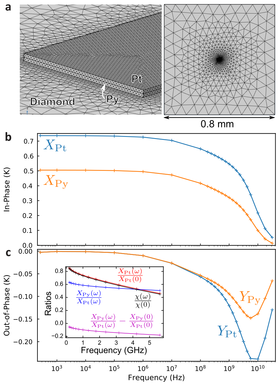
5.3.2 Finite-element simulation
We perform finite-element simulations (COMSOL) of the nanowire’s active region (between the contacts, where the current is concentrated) and the diamond substrate. Figure 6(a) shows the simulated geometry, comprising a diamond substrate (dimensions varied with frequency as discussed below), upon which a 10 nm Py (bottom) / 10 nm Pt (top) nanowire spanning 5.2 0.417 m2 is positioned at the center. We assume the heat is primarily dissipated in the constriction (the nanowire), and that the large-area connection to diamond serves as the dominant heat sink in this system; as such we do not bother to include the leads in this study. Including a “standard” convective heat loss of 25 W/m2K boundary condition on all free surfaces does not significantly alter the results, nor does reducing the mesh density along each axis by a factor of 2.
As per Eq. 51, we introduce an oscillatory power of amplitude =1017 W/m3 and and frequency to the Pt and Py layers. We let the simulation run until it converges to a steady state, then extract the in-phase (, Fig. 6(b)) and out-of-phase (, Fig. 6(c)) amplitudes from the time-dependent temperatures .66 6 Note this single-frequency method is significantly more efficient than performing an impulse response when covering this many decades of frequency.
At lower frequencies, the temperature change penetrates further into the diamond, and a larger diamond volume is required for the results to converge. At the lowest frequency simulated (265 Hz), for example, we employed the 0.8 mm 0.8 mm 0.4 mm volume shown in Fig. 6(a), but a small deviation from adiabatic response is still evidenced by a sub-percent out-of-phase response due to integrator-like behavior as heat reaches the boundaries of the diamond. This phase lag returns at higher frequencies ( Hz) as the heat ceases to efficiently escape the nanowire.
The inset of Fig. 6(c) shows the quantities of interest in Eqs. 67-68, as well as for the total wire assuming . We can now plug this into our expression for the RF current amplitude (Eq. 44 rewritten)
| (69) |
to convert the observed rectified voltage in Fig. 5(a) (at mA) to RF current, using the values , mA-2 from the fit in Fig. 4. Figure 7 shows the frequency dependence of (black curve) along with the absolute calibration range of Eq. 45 (shaded region), highlighting the importance of the frequency-dependent thermal response in our system. If we ignored as in Ref. [12] (e.g.) we would overestimate by up to 65%, and miss a systematic variation of over the probed frequency range. We suspect this correction is smaller in more thermally-isolated systems such as wires on oxide or spin valves, though we note that the thermal transfer function falls off very gradually at high frequencies.
6 Macrospin model
In this section we develop a useful toy model in which the magnetization of the Py layer is assumed to be spatially uniform. Section 6.1 presents the equations of motion, Sec. 6.2 derives the natural frequency for small-angle precession about equilibrium, and Sec. 6.3 derives the magnetization’s linear susceptibility to general oscillatory torques. Finally, we perform simulations to roughly describe the parametrically driven, large-amplitude dynamics in Figs. 3-4 of the main text in Sec. 6.4.
6.1 Equation of motion
We employ the Landau-Lifshitz-Gilbert equation in the low-damping limit, with the spin Hall torque from the Pt layer [11]:
| (70) |
Here, is a unit vector describing the orientation of the magnetization, is the magnitude of the gyromagnetic ratio, is the magnetic permeability of free space, is the effective field (discussed below), is the damping parameter (approximately equal to the Gilbert damping for weak damping and spin transfer torques), is the Bohr magneton, is the fraction of incident spins that are absorbed by the Py layer, is the spin Hall angle of Pt, is the charge current density in the Pt layer (determined by the parallel resistor model of Sec. 5.3.1), is the electron charge, is the thickness of the Py layer, and is its effective saturation magnetization. The effective field
| (71) |
where is the applied field, the shape anisotropy field
| (72) | ||||
| (73) |
with being the elements of a demagnetization tensor (assumed diagonal for simplicity, with ), and
| (74) |
is the spatially averaged field generated by the instantaneous current flowing through the wire, with proportionality constant . For our long wire (aligned along ), we assume , such that is the effective magnetization.
6.2 Small-angle precession frequency
Our first goal is to estimate the resonant frequency for for small-angle precession when the applied field is sufficient to saturate . To do so, we ignore dissipation and current in Eq. 70, and include an applied field with (as in the experiment):
We find the equilibrium values and of and by setting , which gives three equations and three unknowns. Assuming is large enough that leaves only the first equation, which can be written in terms of as
| (78) |
We note that T is required to saturate the magnetization along meaning our mT fields will only slightly raise the magnetization out of the plane. As such, we assume so that . To first order in , this simplifies to
| (79) |
For our system’s effective saturation fields mT and (see Sec. 7), a 35-mT field applied along the NV axis (35∘ out of plane), (2.3∘ out of plane). To find the natural precession frequency , we therefore apply the limit and , to Eq. 6.2, which yields coupled differential equations for and :
| (80) | ||||
| (81) |
with . Using the trial solution
| (82) | ||||
| (83) |
with real-valued amplitudes and yields
| (84) | ||||
| (85) |
from which the amplitude ratio
| (86) |
and resonant frequency
| (87) |
Importantly, this is the same (Kittel) formula one would arrive at with a purely in-plane field, which makes sense in this small- limit. Also, even for our maximal in-plane field mT, , and this ratio increases at lower fields, diverging at , as expected. As such, the -generated stray field power at the NV (i.e., the quantity responsible for the spin relaxation rates) is at least times smaller than that of (and much smaller at the fields of interest).
6.3 Linear susceptibility for magnetization approximately along the in-plane hard axis
We now derive the susceptibility of to an oscillatory drive at frequency . Since we know the magnetization is saturated along to good approximation (and behaves as though for our parameter range; see Sec. 6.2), we consider an applied field for simplicity, and include a general infinitesimal drive torque
| (88) |
of amplitudes and . Equation 70 can then be written (replacing the current-induced terms with this torque) as
| (89) |
In the limit and to first order, so this becomes
or
| (100) | |||||
| (101) |
Using the trial solution
| (102) | |||||
| (103) |
with complex amplitudes and yields an in-plane steady state amplitude
| (104) |
with
| (105) | |||||
| (106) | |||||
| (107) | |||||
| (108) |
The linewidth nominally depends on , but is the dominant effect, and so should remain approximately constant over our (small) field range. Also, torques along and produce qualitatively different lineshapes, in principle enabling a torque vector measurement [15, 16, 11].
6.3.1 Mixdown voltage and FMR fit function
If the applied field is tilted slightly toward , the equilibrium magnetization will gain a small component . As long as , the response should not change to first order (by symmetry77 7 The resonant frequency increases to lowest order, since the anisotropy field maximally opposes the applied field when aligned with .). However such a tilt does provide access to an in-phase anisotropic magnetoresistance (AMR) oscillation with phase delay , amplitude , and in-phase component (see Sec. 4) proportional to the real part of , which can be written (see Eq. 104)
| (109) |
For small-angle precession, the static change in resistance should contribute very little to the FMR signal, but would scale as
| (110) |
which is close in form to Re. As such, FMR spectra are well fit by
| (111) |
with free parameters , , , and .
6.3.2 Expected spectrum of Brownian magnetization noise
A thermal (Langevin) field [17] is typically assumed isotropic, exerting stochastic, uncorrelated torques with a white noise spectrum in all three dimensions. If the torque power spectral densities of each component are (units of rad2 sec-2 Hz-1), then we expect the power spectral density of to be scaled by the magnitude of the susceptibility squared:
| (112) | |||||
6.4 Parametrically driven, large-amplitude oscillations
The transport technique used to measure the signals shown in Fig. 2 of the main text are most sensitive to the most spatially uniform magnetic oscillations. To gain some qualitative intuition about the observed large-amplitude, parametrically driven dynamics, we numerically integrate Eq. 70 with GHz/T (electron g-factor for 10-nm-thick Py [18]), [11], layer resistivity ratio , and nm. From our fits (Sec. 7) we use mT and mT and effective magnetization mT for consistency. The proportionality constant for current-induced field mT/mA is estimated from the required compensation field at 4.08 mA in Fig. 2 of the main text. In order to achieve a similar threshold for parametric oscillations (i.e., not needing unreasonably large currents), we choose , which is approximately half the value estimated from our FMR fits. This discrepancy is under study, but we nominally think it is related to the actual device’s nonuniform magnetization and / or other nonidealities such as material contamination (e.g., oxidization) and roughness.88 8 Macrospin models are often surprisingly accurate in describing actual nanostructured systems, but their results should always be considered with caution.
To mimic the red data in Fig. 2(a) of the text, we apply a field mT along the NV axis, and current
| (113) |
with mA, mA, and stepped from 1-3.5 GHz. At each frequency, the magnetization is initialized to within 0.1∘ of equilibrium (along and canted 1.4∘ out of plane), and evolved for 100 ns to ensure steady state. The time-averaged change in voltage due to magnetoresistance is then calculated as
| (114) | ||||
| (115) | ||||
| (116) |
where is the undriven resistance, and
| (117) |
is the time-dependent resistance change due to precession, with . Figure 8 shows calculated using an integer number of oscillations in the last 10 ns of each simulation. A large-amplitude parametrically driven peak occurs near the second harmonic of the ferromagnetic resonance above 3 GHz, with a skew toward higher frequencies similar to the data in Fig. 2(a) of the main text. The magnitude is also quantitatively similar, corresponding to in-plane precession about the equilibrium offset () amplitude of 30∘ when V, the trajectory of which is shown in inset (i). The peak is positive because the antidamping spin transfer torque (pointing away from the inset plot’s origin) is, on average, larger when the angle is maximal, though the phase of the resistance oscillations lags behind the drive as shown in Fig. 8(ii). Finally, we note the presence of a much smaller directly-driven oscillation at , arising from the small equilibrium value and the oscillatory current-induced field . This feature is visible in Fig. 4(a) of the main text.
6.4.1 Nanowire stray field along NV axis
In this section, we use the NV’s field-dependent electron spin resonance (ESR) to estimate the strength of the stray field along the NV axis when the device is statically magnetized along . Figure 9 shows the photoluminescence (PL) spectra with field mT applied along the NVA axis for (blue data) NVA, (green data) a reference NV having the same orientation as NVA but positioned 5 m from the device, where the stray field is negligible, and (orange data) NVA after the nanowire’s demise, which removed all evidence of ferromagnetism (we suspect due to oxidization or destruction the Py layer). From the difference in fit ESR frequencies (see Table 1), we estimate the axial stray field at NVA most likely lies between and mT, and we use the “dead device” value mT as our best estimate.
Note the differences in the linewidths and contrasts are due in part to imperfect power coupling to the stripline, and inhomogeneity in the external field can only account for a maximum of 2 MHz of deviation between NVA and NV.
| (MHz) | (mT) | |
|---|---|---|
| NVA, magnetized device | ||
| NVA, oxidized device | ||
| NV |
6.4.2 Estimating the parametric precession angle
Knowing the strength of the nanowire’s stray field at NVA (Sec. 6.4.1 above) allows us to estimate the parametric oscillation angle from the reduction in stray field shown in Fig. 3(a) of the main text, using the macrospin approximation. As discussed above, the steady-state trajectory is roughly sinusoidal and highly confined to the plane, so we approximate for simplicity
| (118) | ||||
| (119) | ||||
| (120) | ||||
| (121) |
where is the time-dependent in-plane angle from , is the steady-state amplitude, and nanowire’s drive frequency, equal to twice the parametric response frequency, and is a steady-state phase shift. In this limit, we can calculate the time-averaged magnetization along , which will reduce the stray field experienced by NVA as
| (122) | ||||
| (123) |
where () is the zeroth order Bessel function. Figure 3(a) in the main text shows an increase in the transition frequency of MHz, which corresponds to a decrease in stray field of mT. Assuming the precession is sufficiently symmetric that the stray field orientation remains the same, the fractional change
| (124) |
Using mT from Sec. 6.4.1 at the same external field, we estimate .
Under the same approximations, we can independently estimate from the magnetoresistance signal
| (125) |
When current is sent through the device, with mA and , time-averaging the precession-induced voltage yields
| (126) |
where we have dropped the comparatively small “mixdown” term involving for simplicity (the term contributes to the total signal for this range of parameters, as shown in supplementary Sec. 6.4). In this limit, the peak measurement of V in Fig. 3(a) of the main text ( mA, mA, ) corresponds to . Similarly, the V parametric peak in Fig. 2(a) of the main text ( mA) corresponds to , in reasonable agreement with the macrospin simulation (Sec. 6.4).
7 Ferromagnetic resonance frequencies
Because the spin transfer drive and magnetoresistance signal both approximately vanish when the equilibrium value of is (nearly) parallel to (i.e., the field’s in-plane angle , we cannot measure the ferromagnetic resonance (FMR) frequency directly. Instead, we measure for a set of 8 to 9 small angles spanning (maintaining the out-of-plane angle as in the main text), and then fit the resulting frequencies to a symmetric polynomial to estimate (and a misalignment angle ).
Figure 10(a) shows a “typical” set of spin-transfer-driven FMR spectra with applied field mT, taken as discussed in Sec. 5.2.2, with the Joule heating background (Sec. 5) subtracted. Due to the frequency-dependence of the drive current (see Sec. 5.2.4), we fit only the data near the resonant feature to Eq. 111 to extract the frequency and width . As expected, the signal increases with . Also, as shown in Fig. 10(b), the frequency decreases as approaches zero, consistent with the shape anisotropy maximally opposing the applied field at . Exploiting the mirror symmetry of our geometry, we fit the observed angular dependence in Fig. 10(b) to a low-order symmetric polynomial of the form
| (127) |
with fit constants , , , and offset angle . The offset angle ( for the shown data set) takes on values within of over the usable range of applied fields (14-35 mT). Completing the same analysis at each value of applied field produces the zero-angle frequency data shown in Fig. 10(c). Clear fit systematics preclude the trustworthiness of frequencies so estimated below 14 mT. The “reliable” region (dark symbols) can then be fit to a variety of models to estimate material parameters of the permalloy (Py) layer.
7.1 Macrospin approximation to resonant frequency
To gain immediate insight, we first assume the magnetization simply behaves as a uniformly-magnetized ellipsoid with equilibrium magnetization approximately parallel to . As derived in Sec. 6.2, the resonant frequency for our geometry (Eq. 87)
| (128) |
where is the in-plane component of the applied field. Fitting the “reliable” range of data (blue curve in Fig. 10(c)) yields effective saturation fields mT and mT. The low value of (nominally close to the saturation magnetization) suggests non-uniform magnetic dynamics and / or other nonidealities of the Py layer.
7.2 Lowest-order spinwave approximation to resonant frequency
To get a sense of scale for the potential impact of nonuniform dynamics, we can also perform a fit to an approximate lowest-order (most uniform) spinwave resonance, which has frequency [19, 20]
| (129) |
where is the in-plane component of the applied field, is an effective demagnetizing (dipole) field, is Py’s saturation magnetization, , with exchange constant J/m [21], is the magnitude of the spin wave vector , and
| (130) |
where is the angle between the equilibrium magnetization orientation and , and with device thickness .
For our thin film, we expect to be approximately uniform along [19, 22] (we also ignore the small offset in the equilibrium out-of-plane component ). The nanowire further constrains the longitudinal wavenumber as , with and m deviating slightly from the geometrical length due to effective dipolar boundary conditions on the wire [22, 23]. The remaining relevant wave number is often written in terms of the transverse mode number and an effective width , which we expect to be smaller than the actual wire width when [20, 22, 24]. The lowest frequency (and most spatially homogeneous) mode should have , so we treat the resonances measured in transport as having a wave vector .
Equation 129 effectively contains two fit parameters, and , which themselves are composed of three unknown quantities, , , and . Table 2 shows the fit values of for a wide range of assumed , with the corresponding fits for nm (orange) and m (green) plotted in Fig. 10(c) showing negligible deviation from the macrospin model. As expected, as becomes large, the and from the macrospin approximation (Sec. 7.1). We presume should not be smaller than 50 nm, and the low value of still suggests some nonidealities in the Py layer, which will be the subject of future investigations and higher quality materials deposition. Note that modifying the parameters , , or by factors of order unity does not affect the key results – observed spin transfer threshold for parametric oscillations, observed stray fields (or lack thereof) at the NV, and observed spin transfer damping – of the main text.
| Fixed (nm) | (mT) | (mT) |
|---|---|---|
| 50 | ||
| 100 | ||
| 200 | ||
| 400 | ||
| 800 | ||
| 1600 |
8 Magnon-induced NV spin relaxation rates
In this section, we use the spin-transfer-free relaxation rates measured at a variety of NV probe frequencies and applied fields to estimate the rates at other values of and (i.e., the color scales in Fig. 5 of the main text). The basic idea can be understood by inspecting the phase space of spin wave modes shown in Fig. 11(a). Here, many spin wave mode frequencies (where is the mode wavenumber; see Sec. 7.2) are plotted over our range of applied fields. Importantly, all modes follow the same family of curves to good approximation, meaning one can use a measurement of (taken at the filled symbols) to estimate the relaxation rate at another location along the nearest curve; the quantities that vary the most along these curves are the field, frequency, density of states, and thermal occupancy, all of which are known or can be approximated, as discussed below.

First, we note that the total NV spin relaxation rate [25]
| (131) | ||||
| (132) |
comprises the sum of the NV’s (small) internal rate Hz Hz) (as measured with NVA at mT after the device magnetization disappeared) and the rate kHz) driven by the magnetization’s stray field noise power spectral density (units of T2/Hz), where is the magnitude of the NV spin’s gyromagnetic ratio and the subscript reminds us that it is the fields perpendicular to the NV axis that drive the transitions. Each spin wave mode contributes noise power in proportion to its thermal occupancy , and so we can write
| (133) |
where is a mode-dependent geometrical constant converting occupancy to noise power at the NV (units of T2/magnon), and is a unity-normalized density function (units of 1/Hz) describing how this power is distributed over the frequency domain (i.e., a normalized version of the mode’s power susceptibility, such as Eq. 112).
To simplify the analysis, we assume the mode profiles do not change much over our range of applied fields, so that is approximately independent of field. We do expect to depend on and the exact location of the NV relative to the nanowire, taking on the largest values when is comparable to the wire-NV distance [6, 26].
To simplify further, we note that the observed linewidth MHz of the fundamental mode is approximately constant over our field range, consistent with the behavior predicted by the macrospin approximation (Sec. 6.3). We therefore assume the distributions depend only on and the probe frequency . Figure 12(a) shows an example for applied field mT along the NV axis. Summing across , we then define a total “linewidth-broadened density of modes” , which is shown in Fig. 12(b).
If we imagine following one of the curves in Fig. 11(a), we notice two important quantities change – the mode frequencies and the density of states , suggesting that, if we factor these trends from Eq. 133, we can write
| (134) |
in terms of a “weighting factor”
| (135) |
that should be fairly insensitive to the distance traveled along a given curve. Of particular relevance to the cooling argument of the main text, Fig. 13(a) shows these weights for the direct measurement at point (i) in Fig. 11(a) (cyan circles) as well as the location of maximum cooling (ii) (magenta markers). As we have engineered, both peaks occur at the same value of (7 rad/m), which is a restatement of the fact that we have moved along a curve. Importantly, the distributions at these two extremes look very similar, with individual weights differing by at most 34%, as shown in Fig. 13(b). We remind ourselves that these weights are multiplied by values of expected to oscillate with underneath a smooth envelope, such that the summed effect is more likely of order the -weighted average of the ratio in Fig. 13(b) (i.e., 3%). The presence of additional transverse modes having comparable values of will not have an impact beyond that of Fig. 13(b) unless their mode frequencies deviate from the fundamental mode’s family of curves (gray lines in Fig. 11(a)) by an amount comparable to over the length of the dotted blue line. Even including a more complicated spin wave model or micromagnetic simulations, we do not expect to find modes so strongly deviating from these trends over so small a field range.
We can now convert the directly-measured values of at frequencies and fields (filled circles in Fig. 11(a)) into estimates at other values and using the ratio
| (136) |
The first ratio , with Planck constant , Boltzmann constant , and temperature . The second ratio can be calculated as in Fig. 12, and the final ratio should be comparable to 1, as discussed above. The resulting reconstruction is plotted (solid line) for mT, i.e., the field at which the spin transfer measurements were made in Fig. 11(b). Similar curves can be generated at other values of field, as is plotted on the color scales in Fig. 5 of the main text. Also plotted in Fig. 11(b) are upper and lower bounds (dashed curves) corresponding to worst-case-scenario systematic errors in the final ratio, calculated by assuming the only contributing mode is the one having the largest and smallest values of in Fig. 13(b). Importantly, the expected bias-dependent changes in for Fig. 5(b) of the main text (the probe frequencies of which are indicated by orange and blue squares in Fig. 13) is much smaller than what is observed, and has the opposite trend with applied current.
Figure 14(a) shows the same calculations for effective widths spanning a wide range. As expected, the presence of different transverse mode structure has little effect on these estimates.
Note that, below the fundamental resonance, there is no obvious choice for the blue dashed curves, but there are still modes whose tails contribute to . As such, we have chosen to fix the difference from the fundamental mode frequency (where the density of modes is highest). In this region, the approximation that the final ratio in Eq. 136 is becomes increasingly incorrect – mainly because the occupation at the probing frequency no longer matches the occupation of the nearest magnon modes – as evidenced by exceeding the upper bounds at frequencies below GHz.
This “spin-transfer-free” approximation is valid to the specified tolerances provided the linewidth is constant. When damped by spin transfer, however, we expect the linewidth to broaden, which can redistribute noise away from and potentially reduce without cooling. However, as shown in Fig. 14(b), the broadened density of modes actually increases under the conditions of maximal spin transfer cooling (vertical line), where the linewidth changes by at most a factor of 2. In the worst shown scenario, where the effective width nm, such that the second transverse mode is well above the probe frequency, the broadened density of modes at the probe frequency GHz still increases due to the tails of the modes away from . As increases, the higher-order transverse mode frequencies approach , and is found to increase by as much as . Therefore, if we assume that does not vary significantly over the resonance linewidth (and / or varies linearly), then the sum in Eq. 134 should remain roughly the same or increase (in opposition to the observed trend) as a result of the increased . Combined with the fact that the maximum temperature change due to Joule heating K (see Sec. 5.2.3), we expect this is not a dominant issue.
References
- [1] C. Lee, E. Gu, M. Dawson, I. Friel, and G. Scarsbrook, “Etching and micro-optics fabrication in diamond using chlorine-based inductively-coupled plasma,” Diamond & Rel. Mat. 17, 1292 (2008).
- [2] Y. Chu, N. de Leon, B. Shields, B. Hausmann, R. Evans, E. Togan, M. J. Burek, M. Markham, A. Stacey, A. Zibrov, A. Yacoby, D. Twitchen, M. Loncar, H. Park, P. Maletinsky, and M. Lukin, “Coherent optical transitions in implanted nitrogen vacancy centers,” Nano Lett. 14, 1982 (2014).
- [3] C. Kurtsiefer, S. Mayer, P. Zarda, and H. Weinfurter, “Stable solid-state source of single photons,” Phys. Rev. Lett. 85, 290 (2000).
- [4] R. Verberk and M. Orrit, “Photon statistics in the fluorescence of single molecules and nanocrystals: Correlation functions versus distributions of on- and off-times,” J. Chem. Phys. 119, 2214 (2003).
- [5] J.-P. Tetienne, L. Rondin, P. Spinicelli, M. Chipaux, T. Debuisschert, J.-F. Roch, and V. Jacques, “Magnetic-field-dependent photodynamics of single NV defects in diamond: an application to qualitative all-optical magnetic imaging,” New J. Phys. 14, 103033 (2012).
- [6] T. van der Sar, F. Casola, R. Walsworth, and A. Yacoby, “Nanometre-scale probing of spin waves using single electron spins,” Nature Comm. 6, 7886 (2015).
- [7] P. Elleaume, O. Chubar, and J. Chavanne, “Computing 3d magnetic fields from insertion devices,” in Proceedings of the 1997 Particle Accelerator Conference (IEEE, 1997).
- [8] M. W. Doherty, N. B. Manson, P. Delaney, F. Jelezko, J. Wrachtrup, and L. C. Hollenberg, “The nitrogen-vacancy colour centre in diamond,” Phys. Rep. 528, 1 (2013).
- [9] S. Felton, A. M. Edmonds, M. E. Newton, P. M. Martineau, D. Fisher, D. J. Twitchen, and J. M. Baker, “Hyperfine interaction in the ground state of the negatively charged nitrogen vacancy center in diamond,” Phys. Rev. B 79 (2009).
- [10] S. O. Valenzuela and M. Tinkham, “Direct electronic measurement of the spin Hall effect,” Nature 442, 176 (2006).
- [11] L. Liu, T. Moriyama, D. C. Ralph, and R. A. Buhrman, “Spin-torque ferromagnetic resonance induced by the spin Hall effect.” Phys. Rev. Lett. 106, 036601 (2011).
- [12] V. Tshitoyan, C. Ciccarelli, A. P. Mihai, M. Ali, A. C. Irvine, T. A. Moore, T. Jungwirth, and A. J. Ferguson, “Electrical manipulation of ferromagnetic NiFe by antiferromagnetic IrMn,” Phys. Rev. B 92, 214406 (2015).
- [13] J. C. Sankey, P. M. Braganca, A. G. F. Garcia, I. N. Krivorotov, R. A. Buhrman, and D. C. Ralph, “Spin-transfer-driven ferromagnetic resonance of individual nanomagnets,” Phys. Rev. Lett. 96 (2006).
- [14] Z. Duan, C. T. Boone, X. Cheng, I. N. Krivorotov, N. Reckers, S. Stienen, M. Farle, and J. Lindner, “Spin-wave modes in permalloy/platinum wires and tuning of the mode damping by spin Hall current,” Phys. Rev. B 90 (2014).
- [15] J. C. Sankey, Y.-T. Cui, J. Z. Sun, J. C. Slonczewski, R. A. Buhrman, and D. C. Ralph, “Measurement of the spin-transfer-torque vector in magnetic tunnel junctions,” Nature Phys. 4, 67 (2008).
- [16] H. Kubota, A. Fukushima, K. Yakushiji, T. Nagahama, S. Yuasa, K. Ando, H. Maehara, Y. Nagamine, K. Tsunekawa, D. D. Djayaprawira, N. Watanabe, and Y. Suzuki, “Quantitative measurement of voltage dependence of spin-transfer torque in MgO-based magnetic tunnel junctions,” Nature Phys. 4, 37 (2008).
- [17] W. F. Brown, “Thermal fluctuations of a single-domain particle,” Phys. Rev. 130, 1677 (1963).
- [18] J. P. Nibarger, R. Lopusnik, Z. Celinski, and T. J. Silva, “Variation of magnetization and the Landé g factor with thickness in Ni-Fe films,” Appl. Phys. Lett. 83, 93 (2003).
- [19] B. A. Kalinikos and A. N. Slavin, “Theory of dipole-exchange spin wave spectrum for ferromagnetic films with mixed exchange boundary conditions,” J. Phys. C: Solid State Phys. 19, 7013 (1986).
- [20] T. Brächer, P. Pirro, and B. Hillebrands, “Parallel pumping for magnon spintronics: Amplification and manipulation of magnon spin currents on the micron-scale,” Phys. Rep. 699, 1 (2017a).
- [21] N. Smith, D. Markham, and D. LaTourette, “Magnetoresistive measurement of the exchange constant in varied-thickness permalloy films,” J. Appl. Phys. 65, 4362 (1989).
- [22] C. Bayer, J. Jorzick, B. Hillebrands, S. O. Demokritov, R. Kouba, R. Bozinoski, A. N. Slavin, K. Y. Guslienko, D. V. Berkov, N. L. Gorn, and M. P. Kostylev, “Spin-wave excitations in finite rectangular elements of Ni80Fe20,” Phys. Rev. B 72 (2005).
- [23] K. Y. Guslienko, S. Demokritov, B. Hillebrands, and A. Slavin, “Effective dipolar boundary conditions for dynamic magnetization in thin magnetic stripes,” Phys. Rev. B 66 (2002).
- [24] T. Brächer, O. Boulle, G. Gaudin, and P. Pirro, “Creation of unidirectional spin-wave emitters by utilizing interfacial Dzyaloshinskii-Moriya interaction,” Phys. Rev. B 95 (2017b).
- [25] C. P. Slichter, Principles of Magnetic Resonance (Springer Berlin Heidelberg, 1990).
- [26] C. Du, T. van der Sar, T. X. Zhou, P. Upadhyaya, F. Casola, H. Zhang, M. C. Onbasli, C. A. Ross, R. L. Walsworth, Y. Tserkovnyak, and A. Yacoby, “Control and local measurement of the spin chemical potential in a magnetic insulator,” Science 357, 195 (2017).