A 5.16Gbps decoder ASIC for Polar Code
in 16nm FinFET
Abstract
Polar codes has been selected as 5G standard. However, only a couple of ASIC featuring decoders are fabricated, and none of them support list size and code length . This paper presents an ASIC implementation of three decoders for polar code: successive cancellation (SC) decoder, flexible decoder and ultra-reliable decoder. These decoders are all SC based decoder, supporting list size up to and code length up to respectively. This chip is fabricated in a 16nm TSMC FinFET technology, and can be clocked at Ghz. Optimization techniques are proposed and employed to increase throughput. Experiment result shows that the throughput can achieve up to 5.16Gbps. Compared with fabricated AISC decoder and synthesized decoder in literature, the flexible decoder achieves higher area efficiency.
Index Terms:
Polar code, ASIC, decoding, SCL.I Introduction
Polar codes, proposed by Arikan[1], has been selected as the 5G standard. Although Polar codes with successive-cancellation (SC) decoding is proved to achieve channel capacity in the asymptotic sense, its error-correction performance is inferior to that of low-density parity-check (LDPC) or Turbo codes at short or moderate lengths. SC list (SCL) decoding, regarded as the most efficient decoding algorithm of polar codes, improves the error-correction performance but suffers from low latency and low throughput due to the serial nature of SC. Much effort has been made to optimize the decoding of Polar codes [2, 3, 4, 5, 6, 7, 8, 9]. However, most works lack ASIC implementation and thus bear less practical relevance.
A couple of ASIC featuring decoders are fabricated in [10, 11, 12]. The chip presented in [10] implements the SC decoding algorithm; The chip presented in [11] implements the belief-propagation decoding algorithm. Both of them suffer from mediocre error-correction performance. The chip presented in [12] implements SCL decoding, but constrains the largest list size and largest code length , which limits its application scope.
I-A Motivation and Contribution
This work is motivated by the desire to provide ASIC decoder to support polar codes research and speed up prototype building of 5G communication systems. The ASIC decoder should have low latency and high error-correction performance, and support a wide range of list sizes and code lengths. To satisfy all the desired properties, we integrated three decoders in one chip: SC decoder, flexible decoder and ultra-reliable decoder.
- •
SC decoder is designed for low latency and long code length with ;
- •
Flexible decoder is a SCL decoder with and . The list size of the flexible decoder can be configured during runtime;
- •
Ultra-reliable decoder is also a SCL decoder, designed for ultra-reliable scene with largest code length and list size .
All the decoders support any code rate. This is the first ASIC implemented SCL decoder supporting and .
To improve throughput, several optimization techniques are proposed. We propose a new internal log-likelihood ratio (LLR) messages storage method which can reduce of the internal LLR memory. A serial list processing architecture is proposed to avoid the crossbar of LLR. This can reduce resource and improve timing performance. To improve utilization ratio of processing element (PE), we propose to decode two packages simultaneously, which can improve throughput by . We also recovery decoded bit from partial-sum to save memory.
I-B Outline
The rest of this paper is organized as follows. Section II gives a brief review of polar codes and SC-base decoding algorithms. The proposed ASIC architectures and optimization techniques are presented in Section III. Section IV presents the implementation results and comparison with state-of-the-art works. Section V concludes the paper.
II Polar Code
An polar code has a code length and information bits. The code rate is defined by . The information bits are assigned to the most reliable sub-channels, and the remaining sub-channels are assigned by pre-defined value, typical zero—called frozen bits. The encoding of Polar code can be defined as , where is the source vector, is the generator matrix, defined as , where is the kernel, ⊗ denotes Kronecker power, and .
II-A SC-based Decoders
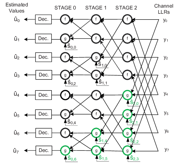
The decoding graph of SC decoder is shown in Fig. 1. The soft values propagate from right to left and the hard bits propagate from left to right. The information vector is decoded sequentially from top to bottom. A hardware-friendly version of soft value updating is carried out in log-likelihood ratio (LLR) domain. Two incoming LLRs ( and ) are combined to produce with the following f-function
| (1) |
or g-function
| (2) |
where is called partial sum (PS). For an SCL decoder, the decoding process is similar to SC decoder except that it keeps paths. When making hard decision for each bit, L paths split into 2L paths, and the ones with smallest path metric (PM) are kept. For list size and bit , the LLR of stage is denoted as and its hard decision is denoted as . The PM updates according to
| (3) |
After all bits are decoded, the path with the smallest PM is selected as the decoding output. To further improve error correction performance, concatenated polar code is proposed. For cyclic redundancy check (CRC) aided SCL (CA-SCL) [13], the most reliable path that passes the CRC is selected as the decoding output. For parity-check SCL (PC-SCL) [14], each parity bit is decided by its parity function rather than by the LLR.
III Architecture
The overview of our ASIC design is shown in Fig. 2. It mainly comprises six units: SC decoder, flexible decoder, ultra-reliable decoder, de-frozen unit, code construction unit and scheduler. Five flexible decoders are integrated in the chip to achieve high throughput. The flexible decoder and ultra-reliable decoder can be configured as SCL, CA-SCL or PC-SCL during runtime. The code construction unit generates frozen bit set for all the three decoders. This can avoid transmission of frozen bit set and support any code rate. The de-frozen unit is responsible to remove frozen bits in source vector. The data-flow is managed by input-scheduler and out-scheduler.
There are four clock domains in the chip. All the six units are clocked by “core clk”, which is generated by clock management unit (CMU). The CMU also generates “LVDS clk” for LVDS(Low Voltage Differential Signaling) sender. LVDS receiver and SPI(Serial Peripheral Interface) bus are clocked by external input clock.
The LLRs are represented in sign-and-magnitude form as in [10]. We denote as the number of bits to represent internal LLR and channel LLR. In our ASIC design, we set for all decoders. We denote as the number of bits to represent PM in metric sorter and PM in memory, respectively. After sorting, the minimum PM will be subtracted from the PM of all list paths and the quantization of PM will be reduced from to . Therefore, of our ASIC is smaller than that of [12].

III-A Flexible decoder
Flexible decoder supports variable list size and code length, with upper limit and . The architecture of flexible decoder is shown in Fig. 3. Channel LLR memory stories the received channel LLRs. Internal LLR memory stories the LLRs generated during decoding process. Good bits are information bits with higher reliability. They are stored and used to reduce path splitting as [8]. In this decoder, we set , , and to preserve the same error performance as a floating-point decoder.

PEs are capable of performing f and g function. If the parallelism of f/g node is larger than , LLR processing is executed in the serial unit. Otherwise, it is executed in the parallel unit. 4-bit is decoded simultaneously in parallel unit by employing multi-bit decision [4]. Up to rate zero nodes [2] and rate one nodes [2] in which all bits are good bits are also decoded simultaneously in parallel unit. Moreover, decoding starts from the first non-frozen bit as [12].
We propose optimization techniques to improve throughput. They are employed in our decodes and presented below.
III-A1 LLR Memory Reduction
In a decoder chip, the internal LLR memory takes up most of the total core area. The in each stage should be stored and will be reused as shown in Fig. 1. The memory size for internal LLR is
| (4) |
In a flexible decoder, we only save internal LLR for every three neighboring stages. The LLRs between these stages can be re-calculated on the fly from the stored LLRs. Therefore, the memory size for internal LLR is reduced to
| (5) |
We can see that almost of internal LLR memory is reduced. To compensate the latency introduced by LLR re-calculation, more PEs are utilized.
III-A2 Serial List Processing
We propose a serial list processing architecture, which executes the LLR processing of different list in serial. As far as we know, all the hardware architecture in literature [3, 4, 5, 9] contains SC decoder cores and execute the LLR processing of different list paths in parallel. Due to LLR exchange among paths, this architecture requires a crossbar of LLR. The crossbar contains -to- multiplexers with complexity growing proportional to .
Our serial list processing architecture executes LLR of different list one by one, thus does not require a crossbar. The LLR exchange among lists can be implemented by exchanging the address of memory. Compared to parallel architecture, serial architecture introduces no extra latency when PE quantity is the same. However, the complexity is reduced and the timing performance will significantly improve especially when list size and PE quantity is large.
At stage , only f/g functions need to be executed as shown in Fig. 1. Therefore, the large number of PEs in serial unit can not be fully used when . For these stages, we apply parallel unit to decrease the latency.
III-A3 Double-Package Mode
Due to the serial nature of SC decoding, the PEs are idle during PM sorting period. The sorting latency is comparable with f/g execution latency when list size is large and multi-bit decoding is used. To improve the utilization ratio of PEs, double-package mode is applied when two packages are decoded simultaneously. When the PM of a package is sorting, the PEs are utilized to execute f/g function for the other package.
We define the decoding time as when only one package is decoded in the decoder. It requires less than to decode two packages under double-package mode. This can improve the throughput by .
III-A4 Decoded-bit Recovery
In general, independent memory for and PS are required in decoder. Their sizes are both bits[3]. However, the memory for is not necessary since is only required when decoded-bits are sent out.
Proposition : For SCL decoder, can be recovered from PS after all bits are decoded.
Proof: We denote as the stored PS vector of stage . Since the serial nature of SC, only elements of will be update simultaneously and need to be stored. After all bits are decoded, the stored PS locates at the right lower triangle of decoding graph (e.g.,the green PS in Fig. 1). We can infer that the final stored
| (6) |
where . A characteristic of generator matrix G is . So, we can induce that
| (7) |
It can be seen as a polar encoding on . According to (7), can be obtained. can be obtained when the last bit is decoded. Thus, can be recovered after all bits are decoded.
The polar encoding can be implemented by bitwise XOR. It takes much less chip area that bits memory. Furthermore, the encoding on PS can be executed in parallel with decoding of next package, has no effect on throughput. Therefore, we use bits memory to save PS and bits memory to save recovered . Compared with general method, we can save bits memory.
III-B SC Decoder
The SC decoder is a simplified version of flexible decoder without path metric management. The SC decoder exploits SSC decoding algorithm [2] and supports code length . Due to the long code length, we set to avoid error-correction performance loss.
III-C Ultra-reliable Decoder
Aiming at , we design an ultra-reliable decoder based on flexible decoder. In the decoder, and is the same as those in the flexible decoder, at stage and at other stages. The main differences between ultra-reliable decoder and flexible decoder are shown below:
III-C1 Serial List Processing
There is a semi-parallel unit besides serial unit and parallel unit in ultra-reliable decoder. The number of PE, subjecting to the number of dependent nodes, can not be added arbitrarily to decrease the latency. Due to the large list size and the number of PE, the latency of serial processing deceases the throughput significantly at some stages. Therefore, four list paths of stage are executed in parallel. These stages are called semi-parallel unit.
III-C2 LLR Memory Reduction
Larger list size requires larger memory size for internal LLR according to (4). Therefore, we save internal LLR for every neighboring stages to save more memory in ultra-reliable decoder. However, four LLR copies of stage need to be stored for supporting semi-parallel unit and increasing the throughput. In total, almost of internal LLR memory are reduced compared with (4).
III-C3 Multi-bit Parallel Processing
Multi-bit decision is also adopted in ultra-reliable decoder. However, only 2-bit and up to rate nodes can be decoded simultaneously.
III-C4 Double-Package Mode
Double-package mode is not supported to save memory.
IV implementation Results and Measurement
This ASIC is fabricated in a 16nm TSMC FinFET technology. The chip area is with , where is the highest frequency of “core clk”. the micrograph and photograph of the chip is shown in Fig.4 and Fig.5.


IV-A Measurement Setup
To test the decoder ASIC, we design a printed circuit board (PCB) which integrates the decoder ASIC and a Xilinx xc7vx690t FPGA. The PCB can be inserted into the PCIE slot of a computer. Test data is generated on the computer, and send to FPGA throughput PCIE. The FPGA acts as a bridge between computer and decoder ASIC.
IV-B Error-Correction Performance and Throughput
The frame error rate (FER) under various list sizes, code lengths and code rates are tested by the designed PCB with bits CRC, and plotted in Fig.6. The codewords are randomly generated, modulated with quadrature phase-shift keying (QPSK) and transmitted over an additive white Gaussian noise channel. As a reference, the floating-point results are also plotted in Fig.6. It can be seen that quantization incurs performance loss less than 0.1dB.

The measured throughputs are summarized in Table. I. The throughput (T/P) is defined by
| (8) |
where is the decoding latency. The highest throughput is Gbps when code rate . The throughput of flexible decoder is even higher than the SC decoder since flexible decoder cores are implemented. In terms of area efficiency, SC decoder is the highest one in the three decoder. Due to the large list size, the throughput of ultra-reliable decoder is much lower than the other two decoders.
| 1/4 | 1/2 | 2/3 | 3/4 | 8/9 | |
|---|---|---|---|---|---|
| , | 1649 | 2599 | 3351 | 3821 | 4786 |
| , | 1750 | 2968 | 3777 | 4245 | 5164 |
| , | 33 | 54 | 70 | 75 | 91 |
IV-C Comparison With State-of-the-Art Fabricated ASICs
The comparison with state-of-the-art fabricated ASICs is shown in Table II. Our SC decoder supports , but SC decoder in [12] [10] only supports . Therefore, it is hard to give a precise comparison for these SC decoders in the table. The flexible decoder and [12] run at the same code rate and length, but the former runs with larger list size and can support larger code length. Even though, the area efficiency of flexible decoder is much higher than the scaled result of [12]. As for ultra-reliable decoder, no fabricated ASIC decoder with has been reported in literature.
| implementation | SC decoder | SC decoder | flexible decoder | ultra-reliable decoder | [12] | [12] | [10] | [11] |
| algorithm | SC | SC | SCL(L=8) | SCL(L=32) | SC | SCL(L=4) | SC | BP(15 iter) |
| code length | 32768 | 32768 | 1024 | 2048 | 1024 | 1024 | 1024 | 1024 |
| code rate | 1/2 | 869/1024 | 1/2 | 1/2 | 869/1024 | 1/2 | 1/2 | 1/2 |
| technology | 16nm | 16nm | 16nm | 16nm | 28nm | 28nm | 180nm | 65nm |
| supply() | 0.9 | 0.9 | 0.9 | 0.9 | 0.9 | 0.9 | 1.3 | 1.0 |
| Frequency() | 1000 | 1000 | 1000 | 1000 | 452 | 308 | 150 | 300 |
| T/P (Mbps) | 2599 | 4442 | 3241 | 54 | 7836 | 65.5 | 49.0 | 1024(2) |
| area() | 0.35 | 0.35 | 2.27 | 0.43 | 0.35 | 0.44 | 1.71 | 1.48 |
| area Eff. () | 7426 | 12691 | 1428 | 126 | 22389 | 148 | 28.7 | 692 |
| Normalized for 16nm(1) | ||||||||
| T/P (Mbps) | 2599 | 4442 | 3241 | 54 | 13713 | 115 | 551 | 4160(2) |
| area() | 0.35 | 0.35 | 2.27 | 0.43 | 0.114 | 0.144 | 0.0135 | 0.0897 |
| area Eff. () | 7426 | 12691 | 1428 | 126 | 120289 | 793 | 40815 | 46377 |
- 1
Area is scaled as , frequency as , where is the technology feature size.
- 2
The throughput is scaled to worst case.
To further evaluate our architecture, we present the synthesis result of the flexible decoder and state-of-the-art decoders in Table III. We re-synthesize one flexible decoder and set for fair comparison. The increases to . The scaled result shows that the flexible decoder outperforms state-of-the-art decoders in terms of area efficiency.
| implementation | This work | [9] | [6] | [7] |
| list size | 8 | 8 | 8 | 8 |
| technology | 16nm | 65nm | 90nm | 90nm |
| Frequency() | 1100 | 722 | 289 | 637 |
| T/P (Mbps) | 713 | 599 | 374 | 123 |
| area() | 0.06 | 3.975 | 7.22 | 3.58 |
| area Eff. () | 11883 | 151 | 51 | 34.4 |
| Normalized for 16nm(1) | ||||
| T/P (Mbps) | 713 | 2434 | 2104 | 692 |
| area() | 0.06 | 0.241 | 0.228 | 0.113 |
| area Eff. () | 11883 | 10124 | 9228 | 6124 |
- 1
Area is scaled as , frequency as , where is the technology feature size.
V Conclusion
In this paper, we present an ASIC implementation of three SC-based decoders for polar code in a 16nm TSMC FinFET technology. To our knowledge, this is the first ASIC implemented SCL decoder supporting and . To improve throughput, several optimization techniques are proposed. Measurement result shows that throughput of the SC decoder, flexible decoder and ultra-reliable decoder can achieve up to Gbps, Gbps and Mbps, respectively. Compared with fabricated AISC decoder and synthesized decoder in literature, the flexible decoder achieves higher area efficiency.
References
- [1] E. Arikan, “Channel polarization: A method for constructing capacity-achieving codes for symmetric binary-input memoryless channels,” IEEE Transactions on Information Theory, vol. 55, no. 7, pp. 3051–3073, July 2009.
- [2] A. Alamdar-Yazdi and F. R. Kschischang, “A simplified successive-cancellation decoder for polar codes,” IEEE Communications Letters, vol. 15, no. 12, pp. 1378–1380, December 2011.
- [3] A. Balatsoukas-Stimming, A. J. Raymond, W. J. Gross, and A. Burg, “Hardware architecture for list successive cancellation decoding of polar codes,” IEEE Transactions on Circuits and Systems II: Express Briefs, vol. 61, no. 8, pp. 609–613, Aug 2014.
- [4] B. Yuan and K. K. Parhi, “Low-latency successive-cancellation list decoders for polar codes with multibit decision,” IEEE Transactions on Very Large Scale Integration (VLSI) Systems, vol. 23, no. 10, pp. 2268–2280, Oct 2015.
- [5] J. Lin and Z. Yan, “An efficient list decoder architecture for polar codes,” IEEE Transactions on Very Large Scale Integration (VLSI) Systems, vol. 23, no. 11, pp. 2508–2518, Nov 2015.
- [6] J. Lin, C. Xiong, and Z. Yan, “A high throughput list decoder architecture for polar codes,” IEEE Transactions on Very Large Scale Integration (VLSI) Systems, vol. 24, no. 6, pp. 2378–2391, June 2016.
- [7] A. Balatsoukas-Stimming, M. B. Parizi, and A. Burg, “Llr-based successive cancellation list decoding of polar codes,” IEEE Transactions on Signal Processing, vol. 63, no. 19, pp. 5165–5179, Oct 2015.
- [8] B. Li, H. Shen, and K. Chen, “A decision-aided parallel sc-list decoder for polar codes,” arXiv preprint arXiv:1506.02955(2015), 2015.
- [9] S. A. Hashemi, C. Condo, and W. J. Gross, “Fast and flexible successive-cancellation list decoders for polar codes,” IEEE Transactions on Signal Processing, vol. 65, no. 21, pp. 5756–5769, Nov 2017.
- [10] A. Mishra, A. J. Raymond, L. G. Amaru, G. Sarkis, C. Leroux, P. Meinerzhagen, A. Burg, and W. J. Gross, “A successive cancellation decoder asic for a 1024-bit polar code in 180nm cmos,” in 2012 IEEE Asian Solid State Circuits Conference (A-SSCC), Nov 2012, pp. 205–208.
- [11] Y. S. Park, Y. Tao, S. Sun, and Z. Zhang, “A 4.68gb/s belief propagation polar decoder with bit-splitting register file,” in 2014 Symposium on VLSI Circuits Digest of Technical Papers, June 2014, pp. 1–2.
- [12] P. Giard, A. Balatsoukas-Stimming, T. C. M¨¹ller, A. Bonetti, C. Thibeault, W. J. Gross, P. Flatresse, and A. Burg, “Polarbear: A 28-nm fd-soi asic for decoding of polar codes,” IEEE Journal on Emerging and Selected Topics in Circuits and Systems, vol. 7, no. 4, pp. 616–629, Dec 2017.
- [13] K. Niu and K. Chen, “Crc-aided decoding of polar codes,” IEEE Communications Letters, vol. 16, no. 10, pp. 1668–1671, October 2012.
- [14] H. Zhang, R. Li, J.Wang, S. Dai, G. Zhang, Y. Chen, H. Luo, and J.Wang, “Parity-check polar coding for 5g and beyond,” 2018 International Conference on Communications (ICC), pp. 1–6, May 2018.