Combining Multiple Optimized FPGA-based Pulsar Search Modules Using OpenCL
Abstract
Field-Programmable Gate Arrays (FPGAs) are widely used in the central signal processing design of the Square Kilometre Array (SKA) as acceleration hardware. The frequency domain acceleration search (FDAS) module is an important part of the SKA1-MID pulsar search engine. To develop for a yet to be finalised hardware, for cross-discipline interoperability and to achieve fast prototyping, OpenCL as a high-level FPGA synthesis approach is employed to create the sub-modules of FDAS. The FT convolution and the harmonic-summing plus some other minor sub-modules are elements in the FDAS module that have been well-optimised separately before. In this paper, we explore the design space of combining well-optimised designs, dealing with the ensuing need to trade-off and compromise. Pipeline computing is employed to handle multiple input arrays at high speed. The hardware target is to employ multiple high-end FPGAs to process the combined FDAS module. The results show interesting consequences, where the best individual solutions are not necessarily the best solutions for the speed of a pipeline where FPGA resources and memory bandwidth need to be shared. By proposing multiple buffering techniques to the pipeline, the combined FDAS module can achieve up to 2x speedup over implementations without pipeline computing. We perform an extensive experimental evaluation on multiple FPGA boards (Arria 10) hosted in a workstation and compare to a technology comparable mid-range GPU.
keywords
pulsar search, frequency domain acceleration search, FPGA, OpenCL2Corresponding author.
1 Introduction
For a large scale global project such as the Square Kilometre Array (SKA) 11 1 www.skatelescope.org, hundreds of research institutes and companies from over ten member countries are enrolled Dewdney et al. (2009). Each research group is assigned a small task such as one or several modules of the overall pipeline. After each module is investigated and optimised, it needs to be integrated with modules from other groups to form the whole pipeline. For software designs, different institutes can use the same operating system such as Linux and development environment. A large number of programming languages can be applied, and the software developers only need to make sure the external application programming interface (API) can be used by other groups.
Field-programmable gate arrays (FPGAs) and Graphics processing units (GPUs) are two main types of accelerators in radio astronomy projects. For GPU development, CUDA and OpenCL can be employed in the development and the details vary based on the GPU brand. In terms of FPGA development, the traditional synthesis flow needs hardware description languages (HDLs) such as Verilog HDL and VHDL, which is hard to understand let alone modify for SKA collaborators (e.g., software engineers and physicists) without expert knowledge in hardware design. Besides the traditional flow, a large number of high-level synthesis tools support a variety of high-level languages (compared to HDLs) such as OpenCL Czajkowski et al. (2012), C/C++, and Java Costabile (2011). In the SKA project, a framework that executes across heterogeneous platforms such as OpenCL is an excellent option for prototyping designs using acceleration hardware. By applying OpenCL, the same kernel codes can be executed on both FPGAs and GPUs without substantial modification, providing the same functionality of the design. While this is very useful, the performance of a single OpenCL design might vary strongly across platforms, due to the difference between the structures of FPGAs and GPUs, and require some ’performance porting’ between different types of devices. The use of OpenCL makes the code more accessible to non-hardware-designers, provides functional portability and easy generational upgrades within a device type.
In this research, we investigate the Fourier domain acceleration search (FDAS) module Ransom (2001) of the pulsar search engine (PSS) within the SKA1-MID central signal processor (CSP). The main function of the FDAS module is to remove the smeared pulsar signals by using the correlation technique Ransom et al. (2002); Jouteux et al. (2002). It consists of two main parts: FT convolution sub-module and harmonic-summing sub-module. The FT convolution module is a compute-intensive application that contains 85 FIR filters, with up to 400 coefficients (or taps). The harmonic-summing module is a data-intensive application, and the main problem is the large number of irregular memory accesses during processing. These two modules have been individually investigated and well-optimised on high-end FPGAs using OpenCL in previous research. The optimised designs can gain better performance and consume less energy on FPGAs than that of GPU designs while meeting the requirements. However, the optimised performance might not be achieved when combining with other modules. More interestingly, optimisation choices might be different when sub-modules are part of a larger pipeline. We investigate in this paper the combination of well-optimised designs, explore the design space and optimise the combination of designs. The main contributions of this research are as follows:
- •
Design Space: explore the design space of combining investigated implementations; three types of data transformation methods are investigated to combine proposed FT convolution and harmonic summing implementations;
- •
Pipeline structure: adopting multiple buffering (double and triple buffering in this research) to improve the performance of investigated combinations;
- •
Multiple Devices: multiple acceleration devices are employed in processing the combined implementations. Different methods of partitioning the workload across devices are investigated.
The rest of the paper is organized as follows. Section 2 provides the details of straight-forward and optimised designs of the FT convolution module and the harmonic-summing module and states the design goals of the FDAS module. In Section 3, the design space of combining optimised modules is explored, and the pipeline structure is investigated on multiple devices. Section 4 presents the experimental evaluation results and their analysis. Finally, the conclusions are given in Section 5.
2 Frequency Domain Acceleration Search
The FDAS module illustrated in Figure 1 is a part of the SKA1-MID CSP element, and the required parameters are listed in Table 2. From the antennas, over 2,000 beams are formed at 4,096 frequency channels per beam. The signals of each beam are processed independently, and each beam needs a dedicated pulsar search engine. Because the dispersion measure, to compensate for signal changes due to travel through interstellar space, is unknown, over 6,000 trial values are tested, and several pulsar search approaches are employed such as time domain acceleration search and frequency domain acceleration search. The FDAS module consists of two main parts: 1) the FT convolution module and 2) the harmonic-summing module. Both these modules have been investigated and optimised for FPGAs before (the FT convolution module in Wang et al. (2016); Wang et al. (2018) and the Harmonic-summing module in Wang et al. (2018)), and we very briefly review the details in this section.
[h] FDAS Module Parameters \topruleParameter Description Value \colrule Number of beams 1000~2000 Number of de-dispersion measure (DM) trails time period of each observation Number of templates (row of the FOP ) Number of channels (column of the FOP) Number of FIR filter taps for each template Total number of harmonic planes Number of candidates per harmonic plane \botrule
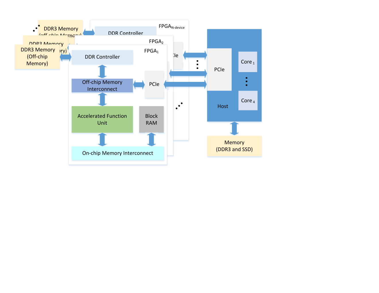
In previous research, different types of acceleration devices were employed to evaluate the performance of the straight-forward and optimised approaches. Two types of Intel high-end FPGAs (Stratix V, referred to as , and Arria 10, referred to as ) are compared with one mid-range AMD R7 GPU, referred to as . The platform specifications are given in Table 2. The FPGA and GPU cards are connected to the host through the PCIe bus, and the structure of FPGA-based platform is depicted in Figure 2. For the FPGA acceleration cards, each one is connected through 8x lane PCIe bus ( use PCIe Gen2.0 and use PCIe Gen3.0). Regarding the GPU board, it uses a 16x lane PCIe bus of Gen3.0. Gen3.0.
[h] Details of CPU, GPU and FPGA Platforms \topruleDevice Terasic DE5-Net Nallatech 385A Sapphire Nitro R7 370 Intel CPU Host (S5) (A10) (R7) (I7) \colruleHardware Intel Stratix V Intel Arria 10 AMD Radeon Intel Core 5SGXA7 GX1150 R7 370 i7-6700K Technology Compute resource 622,000 LEs 1,506,000 LEs 1,024 Stream Processors 8 Processors 256 DSP blocks 1,518 DSP blocks (16 Compute Units) (4 Cores) On-chip memory size 50 53 — 64 Off-chip memory size 2 x DDR3 2 x DDR3 GDDR5 DDR4 Memory interface width 2 x 64-bit 2 x 72-bit 256-bit — Max clock frequency 600 1.5 985 4.2 Max power consumption — 75W 150W — \botrule
Apart from these PCIe card-based platforms, the Intel Xeon Scalable processor with an in-package Arria FPGA from the Hardware Accelerator Research Program (HARP) is employed in this research. The platform, referred to as , has a 14 core Xeon processor at and an Intel Arria 10 GX1150 FPGA, which is the same as the one on the card.
2.1 FT Convolution Module
The core computation part of the FT convolution module is to process points with FIR filters. The basic FIR filter implementation is investigated in both time domain (TDFIR) and frequency domain (FDFIR).
Frequency domain – FDFIR
Naïve TDFIR
The TDFIR filter is a straight-forward implementation of equation 1
| (1) |
where , , and are complex single precision input signals, coefficients, and output results, respectively.
Overlap-add Algorithm based TDFIR
The amount of logic resources and DSP blocks in a specific FPGA are fixed. If the FIR filter size is too large, an FPGA does not have enough logic resources and DSP blocks to parallelise complex multiplications and then fails to achieve a pipeline structure. To make an -tap FIR filter fit into the targeted FPGA and maintain high-performance, we apply the overlap-add algorithm (OLA) to split the coefficient array into a group of sub-arrays Pavel & David (2013).
Frequency domain – FDFIR
Naïve FDFIR
Based on the convolution theorem, Equation (2), the output of an FIR filter can be obtained by the following three steps Steven et al. (1997): 1) Fourier transform of the input array and coefficient array, 2) element-wise multiplication of these two arrays, and 3) inverse Fourier transform of the output array.
| (2) |
where and are Fourier transform and inverse Fourier transform.
Overlap-save Algorithm based FDFIR
For large input size Fourier transforms, such as the targeted two million points () FFT, the on-chip memory of an FPGA is unable to store all points, which makes it impossible to perform the complete process as described in Equation (2) in one go. Hence, we apply the overlap-save algorithm (OLS) to split the input signals into chunks Pavel & David (2013). Each chunk overlaps with its two neighbour chunks, and the extent of the overlap is . For the first input chunk, zero points have to be padded at the beginning. After convolving in frequency-domain, the overlap, which is the first points of each chunk, are discarded.
Optimised Performance
The straight-forward and optimised implementations of a single FIR filter are evaluated, and the execution latencies of these kernels are given in Figure 3. For TDFIR kernels, the value 64 represents a completely parallelised 64-tap FIR filter. The FPGA has 256 DSP blocks and 64 complex SPF multiplications are the largest scale it can parallelise. AOLS is the area-efficient OLS-FDFIR that contains only one FFT engine (radix-4 feed-forward FFT Garrido et al. (2013)). The AOLS kernels have to be launched twice to process one input array. The TOLS is the time-efficient OLS-FDFIR that contains two FFT engines. The number after AOLS and TOLS in the legend of Figure 3 indicates the size of the point chunks.
The experiments in Wang et al. (2016) demonstrated that TOLS-1024 is the fastest among these kernels in implementing one FIR filter. For FIR filters, kernel TOLS-1024 has to Fourier transform the same input array times. The AOLS kernels then become efficient since it can Fourier transform the input array once and then launch times to implement FIR filters.
Using the fastest implementation of the optimised designs (AOLS-2048), the pipeline is slightly extended to include the power calculation of the complex filter outputs and then evaluated on two types of FPGA devices and one GPU device. The results over varying numbers of FIR filters are given in Figure 4. For FPGAs, the results are based on employing three cards, and the same AOLS-2048-P kernel can be replicated 3x times on each and 4x times on each. It can be seen that three cards can execute the FT convolution module in about , and it is 1.3x times faster than the single GPU, which uses significantly more power than three FPGA boards.
2.2 Harmonic-summing Module
The FT convolution output is the Filter-Output-Plane (FOP) that is sent to the harmonic-summing module for candidate detection. In the harmonic-summing module, which is described in Algorithm 1, the FOP is stretched by a group of integers to generate stretch planes (s). The FOP and stretch planes are accumulated to calculate harmonic planes (s) and then threshold-detection logic is applied to collect candidates from each harmonic plane. All operations in the harmonic-summing module are inexpensive operations such as floating-point additions and comparisons with a constant. The FOP takes up to under current requirements, which is tens of times larger than the on-chip memory size of a high-end FPGA, so it has to be stored in the off-chip memory (i.e., DDR RAM on FPGA board) in the FT convolution module. The main issue for this module is the large number of irregular off-chip memory accesses, and we optimised this issue using two approaches: 1) reducing the number of accesses and 2) increasing the used off-chip memory bandwidth Weinhardt & Luk (1999).
(filter-output-plane (FOP))
{initialize the detection output}
for to do
for to do
for to do
stretch {generate the value in stretched plane}
{based on the stretched plane, generate the value in harmonic plane}
detection {threshold-detection logic to identify valid peak signals}
end for
end for
end for
Candidate List
Two types of methods for the processing in the harmonic-summing module were investigated: SingleHP, where a single harmonic plane is processed at a time, and MultipleHP, where multiple harmonic planes are processed simultaneously. The optimised methods are listed below and the parameters are described in Table 2.2. {itemlist}
SingleHP {itemlist}
SingleHP-
MultipleHP {itemlist}
Naïve MultipleHP
MultipleHP-H-
MultipleHP-N-
MultipleHP-R- {wstable}[h] Parameters of harmonic-summing methods \topruleParameter Description \colrule represents single or multiple launch(es) and represents vectrize or replicate the kernel Value of the parellelization factor preloaded data size of the MultipleHP-H method Number of processed columns of all harmonic planes per work-group using MultipleHP-N Number of processed columns of all harmonic planes per work-group using MultipleHP-R Number of processed points of all harmonic planes per work item \botrule
The SingleHP method is a straight-forward implementation of Algorithm 1. The main advantage of MultipleHP over SingleHP is that it is unnecessary to store harmonic planes in the off-chip memory during processing. The MultipleHP-H method is based on the Naïve-MultipleHP method, and it preloads the points with the highest touching frequency in the FOP. Another loading method is MultipleHP-N that loads all necessary points in the FOP that are needed to calculate columns of all harmonic planes. Though these methods can reduce the off-chip memory accesses to some degree, the accesses to the off-chip memory are still irregular.
The MultipleHP-R method is based on the MultipleHP-N method, however, the FOP is reordered and padded to generate the rFOP before processing. In the rFOP, the necessary points in the FOP that are needed to calculate a block of points in all planes are stored in consecutive memory addresses. This makes some points in the original FOP have to be stored in several places in the rFOP, which leads to an increase in the rFOP size. After reordering, the points in the rFOP can be streamed to FPGA during processing. Besides , the parameter is an important factor for the MultipleHP-R method, and it is restricted by the resources of the target FPGA.
These different approaches were implemented using Intel FPGA-based OpenCL. For each method, the parameters for the best performing implementation and the resource usage and kernel execution latencies, including the candidate detection part, are presented in Table 2.2 and Figure 5. The red dot line in Figure 5 is the required time limitation and the execution latencies are for processing half FOP. Kernel MultipleHP-R performs better than the other kernels, however, additional processing has to be done to reorder the standard FOP. The reorder task can be done on both host and device. In the host program, the memory copy function memcpy() can handle this task efficiently. For the OpenCL kernel, there are no such functions and a block of points has to be copied to another place using a for loop. Although the host processor has the advantage over the FPGAs in reordering the FOP, the penalty for transferring data between host and device has to be considered. device has to be considered.
[h] Resource usage and execution latency of the best harmonic-summing kernels on
| \topruleKernel-(Settings) | Logic utilization | RAM blocks | DSP Blocks | Kernel frequency |
|---|---|---|---|---|
| \colruleSingleHP-() | 42% | 28% | <1% | 206.1 |
| Naïve MultipleHP | 17% | 27% | <1% | 227.06 |
| MultipleHP-H- | 19% | 37% | <1% | 235.84 |
| MultipleHP-N- | 17% | 19% | <1% | 276.54 |
| MultipleHP-R- | 30% | 37% | 3% | 196.88 |
| \botrule |
Without including the candidate detection in the compilation and synthesis process, SingleHP- and MultipleHP-R- can be successfully synthesized for the FPGA, however including candidate detection (as done with the kernels in Figure 5) makes the synthesis fail due to exhausted FPGA resources. This is the same type of compromise we will see later when the modules are combined in the pipeline on the FPGA.
3 Combining Modules and Optimisation
3.1 Design Goals
The FT convolution module and harmonic summing module are well-optimised, and each can meet the required time limitation using three high-end FPGAs. The goal of this research is to combine these two modules while meeting the requirements of the FDAS module, especially the time limitation.
As introduced above, the FDAS module contains two main parts: 1) FT convolution and 2) harmonic summing (including candidate detection). The accumulated latency of different parts is the overall latency of the FDAS module in processing one input array, namely the latencies of: the FT convolution (multiple FIR filters and power calculation) , the FOP preparation , and the harmonic summing :
| (3) |
Latency is affected by three factors: the kernel launching overhead , the execution latency of each FT convolution kernel , and the number of times the kernel is launched. Hence, can be expressed as
Depending on the combination of the FDAS sub-modules, might consist of several parts such as discard , transpose , and reorder and can be expressed as
where the data types of and are Boolean and the values depend on the combined sub-module kernels. Latency varies based on the applied method.
Regarding the FOP preparation, it is a module that is added between the FT convolution module and the harmonic-summing module, which is discussed in Section 3.2.
Based on the fastest results in Section 2.1 and Section 2.2, even the achievable is greater than . Because of the limited logic resources on the FPGA, the fastest implementations of two modules cannot be merged into one implementation. There are two alternatives: 1) keep the optimised kernels and 2) modify the optimised kernels to put the whole FDAS module in one FPGA device.
There are two options without modifying the optimised implementations: 1) use multiple FPGA devices or 2) reconfigure the FPGA device several times. For the first solution, the data transfer rate between the host and devices becomes an essential factor. With PCIe Gen3.0 for example, the theoretical latency of loading half FOP ( points) from one device and sending it to another device is about the same as . If the FOP preparation module is assigned to the host processor, it makes the overall pulsar search pipeline impossible to meet the required time limit. Regarding the second solution, it takes over one second for both and to reconfigure the new bitstream file that is over 10x times larger than which leaves alternative 2. If the optimised kernels are modified to make all three modules fit into one FPGA device, becomes unimportant. The three parts of the FDAS module can work in parallel in a pipeline by employing multiple buffering. Taking the triple buffering as an example, each part can process points from different input arrays at the same time, and the slowest section of these three kernels determines the execution latency of a new input array. The combination of these three parts becomes an important issue. In this research, we investigate the suitable combination of the optimised implementations for a given FPGA device. The total number of combinations is the product of the number of FT convolution methods and the number of harmonic-summing methods. These combinations can be categorised into four types: TDFIR + SingleHP, TDFIR + MultipleHP, FDFIR + SingleHP and FDFIR + MultipleHP.
3.2 FOP Preparation
As introduced in Section 2.1 and 2.2, the output plane from the FT convolution and the needed plane for the harmonic summing varies based on different kernel approaches. To make the FT convolution output plane compatible with the harmonic summing input plane, the output from the FT convolution module has to be transformed, and we add an FOP preparation module to connect these two modules. There are three types of transform processing: (a) transpose, (b) discard, and (c) reorder, which are depicted in Figure 6.
For the TDFIR-based FT convolution kernels, each row of the output plane is the output from an FIR filter (Figure 6(a)). However, processing column by column might be more efficient for some harmonic summing kernels. In this case, the output plane has to be transposed.
The output plane of the FDFIR-based FT convolution kernels (Figure 6(b)) contains a number of slices of dummy/invalid points and these points need to be discarded to get the standard FOP.
The MultipleHP-R kernel performs better than other MultipleHP-based harmonic-summing kernels, however, the input plane is not the standard FOP but the reordered FOP (rFOP). To generate the rFOP, the output plane has to be padded and reordered (Figure 6(c)). The reason for padding with dummy data is to make the number of loaded points per clock cycle a power of two, which is more efficient than other numbers.
For different kernel combinations, these three types of transforms can be combined. If the output plane is the same as the needed input plane, the FOP preparation module can be removed. For example, if the FT convolution output plane is the left plane in Figure 6(b) and the needed input is the right plane in Figure 6(c), all these three transforms have to be applied in a certain order (discard + transpose + reorder) in the FOP preparation kernel.
3.3 Pipeline Computing
Instead of processing one input array, the FDAS module keeps running (24/7/365) when it is employed and will process a constant stream of input signals. The main purpose of this research is to optimise the execution latency of multiple input arrays, i.e. the throughput, but not the overall execution latency of a single input array . Therefore, we investigate the pipeline processing of the FDAS module. Given the three sub-modules, the ideal execution latency for each input array in a pipeline, which is the pipeline period, is and the number of required buffers depends on and , which is illustrated in Figure 7. If , double buffering can be employed, and when , it is recommended to adopt triple buffering.
Note that of the two combinations in Figure 7 are the same, but the combination performs better than the combination when employing pipeline processing, as the pipeline stages are more balanced in the latter case. For combinations where , the parallelisation factors of the three combined kernels can be adjusted to reduce to a value smaller than while aiming that is not increased. In other words, the objective of our research here is to minimise within the resource and bandwidth limits of the FPGA by carefully investigating how to best combine and configure the optimised kernels of the sub-modules.
Device Limitation
For most of the accelerators, the FPGA devices are connected to the host processor through the PCIe bus (Figure 2), which is introduced in Section 2. Three major parts can limit the device performance: FPGA resources, off-chip memory, and the data transfer bus.
FPGA Resources
The logic cells, DSP blocks, and (embedded) RAM blocks are three main types of FPGA resources, and the limit of each kind of resource leads to different problems. The logic cells are employed to handle the necessary fixed-point operations and the shift register. The number of DSP blocks decides the number of parallelised floating-point operations such as multiplications. Regarding the RAM blocks, they are the main on-chip memory, and the number of RAM blocks restricts the amount of data that can be stored in local memory during processing.
Off-chip Memory
Two factors regarding the off-chip memory are discussed: 1) data transfer rate and 2) off-chip memory size.
Because the FOP is stored in off-chip memory, the transfer rate between FPGA and off-chip memory affects the overall performance directly. The off-chip memory type and the width of the connected data bus are factors that determine the theoretical transfer rate. The FPGA acceleration cards employed in this research use DDR3 memory and the platform uses DDR4 memory. Regarding the bit-width of the data bus, the card has two memory banks and connects each memory bank with a 64-bit data bus, which has 128-bit data bus in total. Regarding the card, each memory bank is connected with a 72-bit data bus, and the sum of two memory banks is 144. Hence, under the same operation frequency, the data transfer rate of is higher than that of .
The off-chip memory size affects the performance especially when multiple buffering is adopted. Take the triple buffering (in Figure 7) as an example, if the off-chip memory size is not large enough to hold three FOPs but will hold two FOPs, the implementation is restricted to double buffering. In this case, the execution latency for a new input array might be increased to , which is larger than , assuming that (the case for triple buffering).
Data Transfer Bus
The PCIe bus is the main connection between the host processor and FPGA devices. The transfer rate affects the performance especially when the data has to be transferred between the host and the device during processing. It is determined by the generation of the PCIe bus and the number of lanes connected to the FPGA devices. For example, PCIe Gen3.0 (used in the board) provides per lane, while the latest Gen4.0 provides per lane. The number of lanes can vary between 1 and 16 but is usually either 8 (used in the and board) or 16 for FPGA acceleration cards.
Besides the PCIe bus, the Intel QuickPath Interconnect (QPI) is employed in . It is a point-to-point interconnect released by Intel. The QPI can be operated at up to and the data transfer rate can be tens of .
Performance Factors
The performance of the pipelined FDAS module is mainly influenced by three factors: 1) parallelisation factor for each sub-module, 2) maximum frequency of the kernels, and 3) the global memory bandwidth.
Parallelisation Factor
The optimised kernels as discuss in Section 2 almost fully exploit the target devices (such as their logic resources and off-chip memory bandwidth) and some kernels completely exhaust one type of resource such as the TDFIR kernel on consumes all DSP blocks. To integrate several kernels on one FPGA device, the optimised kernels need to compromise each other, and the straight-forward solution is to reduce the parallelisation factors of the optimised kernel. This obviously leads to an increase of the execution latency of the individual kernels.
Kernel Frequency
The high percentage of resource usage of a combined kernel makes it complex and hard to be implemented by the OpenCL compiler and synthesis tools. This affects the maximum kernel frequency at which it can run, which directly influences the performance.
Off-chip Memory Bandwidth
In pipeline computing, two or three kernels are executed simultaneously (Figure 7). If the total needed off-chip memory bandwidth surpasses the theoretical off-chip memory bandwidth, these kernels might not perform as fast as when executed. In this case, the maximum execution latency is increased and the performance drops.
3.4 Host and Device
Data Transfer Approaches
For FPGA-based OpenCL, there are mainly two types of data transfer approaches between host and accelerator (FPGA). 1) general buffer transfer and 2) shared virtual memory (SVM).
General Buffer Transfer
In an OpenCL host program, a buffer object (one-dimensional) can be transferred between the device off-chip memory (i.e., OpenCL global memory) and the host memory using the clEnqueueReadBuffer and clEnqueueWriteBuffer functions. For two- or three-dimensional buffer, the clEnqueueReadImage and clEnqueueWriteImage are employed. The transfer is realised via the PCIe bus and the rate depends on its specification, see above.
Shared Virtual Memory
Using shared virtual memory (SVM) is a technique to extend the (OpenCL) global memory region into the host memory region. It is supported by the OpenCL 2.0 specification, and the host processor and device(s) need a shared memory system. Since the and devices have no physical shared memory with the host and the SVM technique is not supported there. For the Intel Xeon processor platform with an integrated Arria 10 FPGA, referred to as Xeon+FPGA, the FPGA and processor are in the same package. An illustration of this is given is Figure 8. Inside the FPGA, the accelerated function unit (AFU) is available to be programmed by the developer, the other interfacing blocks are provided by Intel. The core cache interface (CCI) provides a base platform memory interface that exposes physical channels as a single, multiplexed read/write memory interface. The embedded FPGA is connected to the computer system memory (DDR4) through several physical channels such as PCIe and Intel QPI.
The memory properties factory (MPF) block is optional. When it is employed, it is instantiated as a CCI-to-CCI bridge, maintaining the same interface but adding new semantics. The main advantage of MPF is that it can translate the virtual address to a physical address and the FPGA and CPU can share pointers with each other.
SVM-based transfer is about 2x times faster than that of the general buffer-based transfer. By adding the FPGA to the chip-package, the physical design has to compromise with many additional constraints, and the performance of the processor part might not provide the same performance as the independent package processors of the same technology.
Tasks on the host
The FPGA devices are employed as the accelerator, so naturally distributing and balancing tasks between the host and the device are investigated. Due to the usual performance penalty for transferring data between host and device, it is recommended to execute most or all tasks on the device. However, there are situations where data has to be transferred back to the host during processing.
1) The execution latency of a task on the host is significantly faster than that on the device.
Although FPGA devices perform better than the host in a wide range of applications, they still have a weak point in serial processing. If a task is arranged to be executed by the host, the data transfer rate between the host and devices becomes the main issue. Hence, when determining the performance advantage of the host processor or FPGAs, the inflicted data transfer delay needs to be considered in the analysis.
2) Data dependency of using multiple devices
This situation happens when multiple devices are employed in executing the same input array. The host can then become the master that needs to manage the dependences and communications between the sub-tasks and the devices. Of course, the ideal case in designing the FDAS module is to avoid transferring data between the host and devices while processing as much as possible.
3.5 Multiple Devices
When employing more than one FPGA device for the acceleration, there are two obvious approaches: using 1) the same configuration (bitstream) file (single) or 2) different configuration files (multiple) for the programming of the FPGA devices.
Single Configuration File
Single Input Array
Multiple devices for a single input array can be necessary if . Except for the MultipleHP-R method in Section 2.2, the optimised harmonic-summing implementations on a single device take longer than the required time limit. When multiple devices () are employed, the harmonic-summing task can be split into independent parts and each FPGA device processes of the FOP. In this case, the ideal execution latency drops to .
For the FT convolution module and FOP preparation module, each of the devices generates the full FOP, and it is unnecessary for a device to communicate with other devices while processing. Processing a single input array while all devices are configured with the same bitstream file, the same FOP is generated times.
Multiple Input Arrays
For multiple input arrays, the host sends different input array to FPGA devices and input arrays are processed in parallel. Compared with a single device, the ideal execution latency for multiple devices reduces to ,
Hence, the multiple input arrays approach has a theoretical advantage when .
Multiple Configuration Files
For some combinations, the FT convolution and harmonic-summing have to compromise with each other by reducing their parallelisation factors or scales. This leads to a decrease in performance for both parts. By using multiple devices, each device can be configured with one or two functions while taking full advantage of the device resources. In Figure 7, each stage can be assigned to a device and the number of buffering equals the number of devices. For example, when , three devices need to be installed and each device is configured with only one module.
The main problem with this method is the frequent communication between the host and the devices. The host needs to keep organizing data between different devices. This method requires a high transfer rate between the host and devices such as high generation PCIe and QPI.
3.6 A Case Study
Before we systematically evaluate the pipeline design and the many combinations of the different sub-module kernels, let us have a closer look at the combination of the FDFIR+MultipleHP-N kernels as a case study. The execution latency of one input array using three devices is depicted in Figure 9 (top). Three devices are configured with the same file and the harmonic-summing part of each device processes of a half-FOP. The FDFIR filter is parallelised twice (i.e., two filters working in parallel), so the FT convolution kernel needs to be launched times (as there are 42 filters to be applied). Ignoring the FT convolution kernel launching overhead, the execution latency is . The FOP preparation kernel contains discard and transpose, and the harmonic summing kernel processes of the overall task.
As can be seen in the basic execution latency (top), but smaller than . Based on the discussion in Section 3.3, we can infer the execution latency of multiple input arrays using triple buffering. Ideally, the execution latency of each part remains the same as that of executing one input array. The time cost for one new input array is in this example, Figure 9 (Middle).
However, the real execution latency of multiple input arrays takes much longer than the ideal case. The real result and details are given in Figure 9 (Bottom) as well. When the FOP preparation part is processing, the FT convolution part is severely affected, and the is increased as well. Because two FIR filters are working in parallel, the discard kernel is launched twice for two output groups. In the zoomed in part, during the discard processing, the FT convolution kernels are launched 8x times to process the next input array using 16 FIR filters, and the FT convolution kernel is launched with the transpose kernel. The average value of to is larger the that of to and is several times larger than others. The value of is about the same as .
The main reason for the stretch of to is the limited global memory bandwidth (GMB) of the FPGA device. The discard, transpose, and FT convolution kernels all depend heavily on the GMB. When two of them are processing at the same time, the needed GMB exceeds the device GMB. For the transpose kernel, it exhausts the device GMB while processing alone. When the transpose and FT convolution kernels are launched together, the FT convolution kernel is pended until the transpose kernel has been finished. When the three parts are processing in parallel, the value of will be larger than that of in the zoomed part in Figure 9. In real processing, the FT convolution becomes the dominant kernel and it determines the time delay until the next new input array can be processed (i.e., the pipeline period).
4 Experimental Evaluation
This section experimentally evaluates the design space of the FDAS module pipeline, by considering a large number of combinations of the optimised kernels of the sub-modules and their design parameters. The advantage of the multiple buffering technique is evaluated and multiple acceleration devices are employed to accelerate the FDAS module. The combinations are assessed according to their resource usage, execution latency, and energy dissipation and power consumption.
4.1 Resource Usage
High-end Arria 10 FPGAs (Nallatech 385A with Intel Arria 10 GX1150, in Table 2) are employed for the experiments. All combinations are implemented using Intel FPGA-based OpenCL, and all combined FDAS kernels are compiled using AOCL version 16.0.0.222.
For the FT convolution module, the OLA-TD and OLS-FD methods, in Section 2.1, are used. The OLA- kernel, which parallelises complex SPF multiplications, and the AOLS-, which split the input array into a group of chunks whose each length is , are employed to combine with harmonic-summing modules. Taking the OLA-128 kernel as an example, it has to be launched four times to implement a 421-tap FIR filter, and its execution latency is the same as would be for a 512-tap FIR filter, as 91 taps are unused (set to zero).
For the harmonic summing modules, the SingleHP- kernel is selected for the SingleHP method and the Naïve-MultipleHP, MultipleHP-N-, and MultipleHP-R- are chosen for the MultipleHP method. The parallelisation factors of the harmonic-summing module are the largest values that can be compiled successfully by the AOC when combining with the FT convolution module. The MultipleHP-H method is based on the Naïve-MultipleHP method and the best-performing implementation, which is MultipleHP-H-, cannot be combined with other kernels as it exhausts the available FPGA resources. When the is decreased to reduce resources, it performs worse than the Naïve-MultipleHP kernel, so it is not considered in this research.
In summary, for the two types of FT convolution and the four types of the harmonic-summing, there are a total of eight FDAS combinations, listed in detail in Table 4.1. The table also provides resource usage and achievable frequencies of these combinations. Because each of the FT convolution and harmonic-summing parts contains at least one kernel, there are two or more independent kernels in the FDAS module. Each kernel in the FDAS module is compiled as an independent kernel. To arrange multiple independent kernels in a target FPGA, the compiler has to add more restrictions than compiling a single kernel. Although some successfully compiled kernels use less than half of the device resources, the parallelisation factors still cannot be increased as the compilation then fails. For each of the combinations in Table 4.1, several parallelisation factors are tested, and the combination with the fastest execution latency is recorded. Taking combination FDFIR+MultipleHP-R as an example, AOLS-1024, AOLS-2048, and AOLS-4096 are combined with MultipleHP-R-, MultipleHP-R-, MultipleHP-R-, and MultipleHP-R-, which are 12 combinations in total. Among these 12 combinations, only three combinations can be successfully compiled. Of these three combinations, AOLS-2048+MultipleHP-R- provides better performance than the other successfully compiled combinations such as AOLS-1024+MultipleHP-R-, hence it is the one recorded in the table.
[h] Resource usage of the combined FDAS kernels \toprule FT Convolution FOP preparation Harmonic-summing Frequency Logic DSP RAM module module module utilisations blocks blocks \colrule TDFIR OLA-128 – Naïve-MultipleHP 207.8 25% 44% 42% OLA-256 – Naïve-MultipleHP 207.1 32% 86% 64% OLA-128 transpose MultipleHP-N-(1) 159.1 37% 43% 56% OLA-128 transpose+reorder MultipleHP-R- 182.2 47% 46% 52% OLA-128 – MultipleHP-R- 171.9 37% 46% 40% OLA-128 – SingleHP- 179.6 45% 44% 49% FDFIR AOLS-2048 discard+transpose Naïve-MultipleHP 178.4 41% 23% 78% AOLS-2048 discard+transpose MultipleHP-N- 175 35% 12% 66% AOLS-2048 discard+transpose MultipleHP-R- 180 49% 15% 56% +reorder AOLS-2048 – MultipleHP-R- 185.2 35% 15% 42% AOLS-2048 discard SingleHP- 196.5 37% 23% 70% \botrule
[h] Resource usage and kernel frequency of independent and combined implementations
| \topruleKernels | Frequency () | Logic utilization | DSP blocks | RAM blocks | ||||||||
|---|---|---|---|---|---|---|---|---|---|---|---|---|
| FT | HM | Comb. | FT | HM | Comb. | FT | HM | Comb. | FT | HM | Comb. | |
| \colruleOLA-128 + | 267.4 | 227.06 | 207.9 | 21% | 17% | 25% | 42% | <1% | 44% | 27% | 27% | 42% |
| Naïve-MultipleHP | ||||||||||||
| OLA-128 + | 267.4 | 206.1 | 179.66 | 21% | 42% | 45% | 42% | <1% | 44% | 27% | 28% | 49% |
| SingleHP- | ||||||||||||
| OLA-128 + | 267.4 | 196.9 | 171.9 | 21% | 30% | 37% | 42% | 3% | 46% | 27% | 37% | 40% |
| MultipleHP-R- | ||||||||||||
| AOLS-2048+ | 252.3 | 196.9 | 185.2 | 16% | 30% | 35% | 11% | 3% | 15% | 32% | 37% | 42% |
| MultipleHP-R- | ||||||||||||
| \botrule | ||||||||||||
Among these combinations, the OLA-128+Naïve-MultipleHP and OLA-128+SingleHP- do not require the FOP preparation kernel. For combinations that contain the MultipleHP-R- kernel, if the FOP preparation task is assigned to the host processor, the FOP preparation module does not need to be implemented in the FPGA. The resource usage and kernel frequency of independent and combined implementations of these four kernels are given in Table 4.1. As expected, the frequency of the combined kernel is lower than each of its element kernels. The DSP block usage is slightly larger than the sum of element kernels. The logic cell and RAM blocks utilisations of a combined kernel are larger than that of each element kernel, however, smaller than the sum of all element kernels. The reason is that the default BSP package (i.e. interfacing IP blocks) costs logic cells and RAM blocks but is not using any DSP blocks and is incurred only once, independent of the number of instantiated kernels.
4.2 Latency Evaluation
We experimentally evaluated all the combinations of Table 4.1 and their execution latencies are given in Table 4.2. Only the single configuration file approach of Section 3.5 is employed in this section. The recorded values are the execution latencies of processing one input array ( complex SPF points) while applying 42 FIR filters (half of the FOP). Both serial processing and processing using the multiple buffering technique were evaluated. For multiple devices, only the multiple buffering-based processing approach is tested. The major positive observation from the results in Table 4.2 is that by applying the multiple buffering technique, the same kernel combination can achieve up to 2x speedup over non-multiple buffering based processing.
Except for the OLA-256+Naïve-MultipleHP combination, all combinations that contain the OLA-TD method apply the OLA-128 kernel. The value 128 is the largest number of power of two that can be implemented within the combination. For the combination that contains the MultipleHP-R method, the FOP preparation module is evaluated by executing on both host processor or FPGA device(s).
For combination AOLS+Naïve-MultipleHP and combination AOLS+MultipleHP-N, the is larger than , so the single configuration file with single input array approach (in Section 3.5) is applied to split the harmonic-summing task evenly for multiple devices, in this research, see the last two rows of Table 4.2. For the configuration parameters of harmonic-summing kernels, the applied values are the largest that can be successfully compiled by AOC for the FPGA. For the remaining combinations on three devices, they all process multiple input arrays in parallel.
[h] Execution latency of combined kernels on cards
| \toprule FT Convolution | FOP preparation | Harmonic-summing | No multiple | Multiple | Pipeline | Multiple devices | |
| module | module | module | buffering | buffering | period | ||
| () | type | () | |||||
| \colrule TDFIR | OLA-128 | – | Naïve-MultipleHP | 2,121 | Double | 1,698 | 568 |
| OLA-256 | – | Naïve-MultipleHP | 1,278 | Double | 854 | 286 | |
| OLA-128 | transpose | MultipleHP-N-(1) | 2,916 | Double | 2,219 | 742 | |
| OLA-128 | transpose+reorder | MultipleHP-R- | 3,917 | Double | 1,935 | 647 | |
| OLA-128 | transpose+reorder | MultipleHP-R- | 2,727 | Double | 2,052 | 686 | |
| (in host) | |||||||
| OLA-128 | – | SingleHP- | 2,662 | Double | 1,966 | 657 | |
| FDFIR | AOLS-2048 | discard+transpose | Naïve-MultipleHP | 856 | Double | 570 | 190 |
| AOLS-2048 | discard+transpose | MultipleHP-N- | 976 | Double | 661 | 224 | |
| AOLS-2048 | discard+transpose | MultipleHP-R- | 8,780 | Double | 6,630 | 2,219 | |
| +reorder | |||||||
| AOLS-2048 | discard+transpose | MultipleHP-R- | 972 | Double | 633 | – | |
| +reorder (in host) | |||||||
| AOLS-2048 | discard | SingleHP- | 786 | Double | 682 | 237 | |
| AOLS-2048 | discard+transpose | Naïve-MultipleHP | Triple | ||||
| AOLS-2048 | discard+transpose | MultipleHP-N- | Triple | ||||
| \botrule | |||||||
Except for the FDFIR+MultipleHP-R combination, the FDFIR-based combinations perform better than these TDFIR-based combinations . For combinations that contain the OLA-128 kernel, the execution latencies of the FT convolution part are all around , which makes them noncompetitive with FDFIR-based combinations.
Regarding the FDFIR+MultipleHP-R combination, even though the MultipleHP-R method is the fastest among the proposed harmonic-summing methods, the FOP preparation part is inefficient and the FPGA-based implementation is slower than using the host processor. It takes on the host processor and over on an device, which is over 12x times slower. For the FPGA-based implementation, the reorder part in the FOP preparation kernel has to leave enough resources for the main operations and it cannot be parallelised with a large parallelisation factor. This makes the execution latency of the FOP preparation part grow up to . If the FOP preparation task is moved to the host processor, it can process one input array at a time using all threads, and the pipeline computing on multiple devices becomes impossible. By considering the FOP reordering, the advantage of the MultipleHP-R method in low execution latency disappears.
Xeon+FPGA (HARP) and GPUs
The Intel (Xeon+FPGA) platform, as introduced in Section 2, supports SVM-based data transfer and it is especially interesting to evaluate the combinations that require reordering on it. We evaluated the FDFIR+MultipleHP-R combination (AOLS-2048+MultipleHP-R-), and the results are given in Table 1. The same kernel can achieve higher kernel frequency on than on the system. While the execution latency of each FIR filter of the FT convolution module on is shorter than on , the kernel launching overhead on is higher, which makes the total execution latency of 42 FIR filters longer than that on . The main reason is that the host processor part of the performs worse than . Regarding the FOP preparation module, which is processed on the host processor, the SVM transfer on is about 1.7x times faster than the general transfer on . However, the performance of the host Xeon processor is over 1.6x times worse than that of the independent . This weakens the advantage of SVM-based implementation over the general transfer based implementation. It can be seen that the overall on the platform is 6% lower than that on the .
| \toprulePlatform | SVM | Kernel frequency | ||||
| transfer | ||||||
| \colrule | Yes | 225.0 | 347 | 560 | 122 | 1,029 |
| No | 185.2 | 190 | 633 | 149 | 972 | |
| \botrule |
Regarding the GPU, since the single work-item kernels such as candidate detection and FOP preparation are efficient for GPUs, we only compare the combinations that consists of NDRange kernels to not distort the result in favour of the FPGAs. The details of the execution latencies of the GPU-based combinations are given in Table 2. The parallelisation factors are for the FPGA-based kernels and some of them do not work for GPU-based kernels. Though supports running multiple kernels currently, the large number of work-groups of FT convolution kernels and harmonic-summing kernels make it fail to execute multiple kernels concurrently. It can be seen that the pipeline period of a single is over 1.35x times slower than that of , however, three cards provider better performance than . Also, remember that the implementation does less work as candidate detection is not included.
| \topruleFT Convolution | FOP preparation | Harmonic-summing | Speedup of | |||
| module | module | module | () | () | over | |
| \colruleNaïve-TDFIR | – | Naïve-MultipleHP | 909 | 36 | 945 | 3.33 |
| Naïve-TDFIR | – | SingleHP | 909 | 20 | 929 | 1.41 |
| AOLS-2048 | (in the host) | MultipleHP-R (no CD) | 67 | 20 | 720 | 1.05 |
| \botrule |
Less Filter Coefficients
Among the TDFIR-based combinations, OLA-256+Naïve-MultipleHP is the fastest that is comparable with FDFIR-based combinations. If the average FIR length can be reduced, the performance of the TDFIR-based combinations become comparable with those of the FDFIR-based combinations. The execution performance of combinations with reduced is given in Table 3. Since the experiments so far showed that is dominating in the FDAS module for the TDFIR-based combinations, the decrease of directly leads to a reduced execution latency. Still, the of a TDFIR-based combination, after reducing , might be still be longer than that of FDFIR-based combinations. However, the sum of for the FDFIR-based combination can be larger than the of the TDFIR-based combination.
| \toprule | OLA-128+ | OLA-128+ | OLA-128+ |
|---|---|---|---|
| Naïve-MultipleHP | MultipleHP-N-(1) | SingleHP- | |
| \colrule421 | 568 | 742 | 657 |
| 256 | 283 | 370 | 328 |
| 128 | 142 | 226 | 235 |
| \botrule |
4.3 Energy Dissipation and Power Consumption
In this section, we measure the power consumption and energy dissipation of the kernels on the cards. Since we have no physical access to the Intel Xeon+FPGA platform, we were not able to measure those metrics on that platform. Regarding the device, we measure the overall system power consumption in idle status , including FPGA device(s), and the running power when the system is executing kernels on FPGA device(s). The real power consumption can be achieved by calculating the difference of and . When an card is installed in the host, it costs about without launching any kernels. In this case, if the kernel is launched on a single FPGA, only one FPGA device is installed. For kernels running on three devices, three FPGA acceleration cards are installed. To make sure the measured is stable, each combination is launched hundreds of times using a loop, which takes longer than one minute. The power consumption is measured using a plug-in power meter (Ego smart socket ESS-AU). When a device is configured with a new bitstream file, the might be changed slightly. To remove this interference factor, the power consumption of each combination is measured by 1) first shutting down the host for a minute to cool down the host and device(s), 2) boot the system, and 3) execute the kernel directly.
The power consumption and energy dissipation of different types of combinations on a single device are given in Table 4. The overall energy dissipation () and absolute energy () dissipation are calculated based on , , and kernel execution latencies for one input array, where is the latency using the multiple buffering technique in Table 4.2 (using 42 FIR filters). Based on the number of installed devices the power consumption in idle status are and .
| \topruleFDAS module | Pipeline | Overall | Absolute | |
| Combinations | computing | energy | energy | |
| () | () | |||
| \colruleFDFIR+MultipleHP-R | No | 66 | 180.2 | 46.4 |
| (FOP preparation in host) | ||||
| FDFIR+MultipleHP-R | No | 59 | 519.2 | 88 |
| FDFIR+Naïve-MultipleHP | No | 59 | 50.6 | 8.6 |
| Yes | 60 | 30.6 | 6.3 | |
| FDFIR+MultipleHP-N | No | 60 | 58.6 | 10.7 |
| Yes | 63 | 35.9 | 8 | |
| FDFIR+SingleHP | No | 62 | 48.7 | 10.2 |
| Yes | 64 | 43.5 | 10.2 | |
| TDFIR+SingleHP | No | 60 | 159.7 | 29.3 |
| Yes | 69 | 135.7 | 39.3 | |
| TDFIR+Naïve-MultipleHP | No | 57 | 120.8 | 17.0 |
| Yes | 59 | 100.2 | 17.0 | |
| TDFIR+MultipleHP-N | No | 57 | 166.2 | 23.3 |
| Yes | 59 | 130.9 | 22.2 | |
| \botrule |
The first observation is that the power consumption does only vary between and , whereas the energy dissipation varies significantly more, which is of course due to the large difference in execution latencies (see Table 4.2). For the same combination, the overall energy dissipation by applying pipeline computing is lower than that without pipeline computing. Regarding the absolute energy dissipation, applying pipeline computing costs less energy for most of the combinations. For the TDFIR+SingleHP and TDFIR+Naïve-MultipleHP combinations, the absolute energy dissipation of the pipeline computing based implementations are about the same as those of without pipeline computing. The reason is that the longest part of these combinations, which is , takes a high proportion in the overall execution latency, hence the pipeline is not balanced enough to provide more benefit. FDFIR+SingleHP is the only combination that consumes more energy using pipeline computing. The main reason is that the ratio of is over 75%, making the execution latency for a single input array close to the pipeline period, in other words, the pipelining in not efficient. In addition, the power consumption of pipeline computing is larger than that without pipeline computing, likely due to the need of additional buffers and the implicit communications and the fact that more processing is happening at the same time.
When three are installed to accelerate the FDAS module, the is about 2x times higher than those using the single device, which is given in Table 5. The power consumption of the FDFIR+SingleHP combination is the highest among these implementations, however, the power consumption for three cards is only (), where is . It can be found that it is smaller than that of a single mid-range GPU device, not to mention high-end GPU platforms, which can cost up to per device. For the TDFIR+SingleHP combination on GPU (in Figure 2), the power consumption for one card is , which is larger than the value in Table 5, which is ().
| \topruleFDAS module | Overall energy | Absolute energy | |
|---|---|---|---|
| Combinations | () | () | |
| \colruleFDFIR+SingleHP | 133 | 30.3 () | 10.4 () |
| FDFIR+Naïve-MultipleHP | 128 | 24.3 () | 7.4 () |
| FDFIR+Naïve-MultipleHP | 126 | 38.7 | 11.4 |
| (1/3 of FOP) | |||
| FDFIR+MultipleHP-N | 123 | 27.6 () | 8.7 () |
| TDFIR+SingleHP | 117 | 76.8 () | 18.4 () |
| TDFIR+Naïve-MultipleHP | 108 | 61.3 () | 10.8 () |
| TDFIR+MultipleHP-N | 111 | 82.1 () | 16.3 () |
| \botrule |
By installing three devices, the overall energy dissipation of processing one input array drops when compared with single device-based processing. However, the absolute energy dissipations for FDFIR-based combinations are all increased to some degree (ratio is given in brackets). For the TDFIR-based combinations, the absolute energy dissipations are all decreased. For the FDFIR+Naïve-MultipleHP combination, the implementation that processes one input array on three devices (each device processes 1/3 of half FOP) costs more energy than the implementation that processes three input arrays on three devices. Although the processing one input array on three devices needs less power, the same FT convolution and FOP preparation tasks are redundantly executed three times to avoid communication. Among these combinations, the absolute costs of FDFIR+Naïve-MultipleHP on the single device and three devices are both the smallest, so is the execution latency in Table 4.2.
Regarding the reduction of the average tap number , when is reduced from 421 to 128, the power consumption and energy dissipation of TDFIR-based combinations are decreased, and the overall energy consumption is up to 3.9x times less than that of the original implementation, which is shown in Table 6.
| \topruleFDAS module | Overall energy | Absolute energy | |
|---|---|---|---|
| Combinations | () | () | |
| \colruleTDFIR+SingleHP | 119 | 27.965 | 7.11 |
| () | () | ||
| TDFIR+Naïve-MultipleHP | 114 | 25.76 | 5.65 |
| () | () | ||
| TDFIR+MultipleHP-N | 110 | 15.62 | 2.982 |
| () | () | ||
| \botrule |
5 Conclusions
In paper we have investigated the combination of two well-optimised pulsar search modules: the FT convolution module and the harmonic-summing module. We explored the design space of the FDAS module combinations with different conditions and parallelisation factors using OpenCL. An FOP preparation module that transforms the FOP based on the demand of the two neighbouring modules was added to connect them. We also investigated multiple buffering strategies and assigning the tasks to multiple devices. As expected, after combining the well-optimised kernels, the frequency of the combined kernel was slower than any of its element kernels. The evaluation showed that the method with the best independent individual performance might not provide good performance when combined with other modules. Applying the multiple buffering technique, the combination kernel gains up to 2x times processing speedup. Among the evaluated combinations, the FDFIR+Naïve-MultipleHP performed best and it needed less power and cost less energy than any other investigated combination. Most of the TDFIR-based combinations perform worse than the FDFIR-based combinations. When the average length of the FIR filters can be reduced, the TDFIR-based combinations showed a high potential in achieving higher performance while costing less energy.
Acknowledgment
The authors acknowledge discussions with the TDT, a collaboration between Manchester and Oxford Universities, and MPIfR Bonn and the work benefitted from their collaboration. We sincerely thank Intel for the donation of development tools and hardware access, especially access of the HARP systems. We gratefully acknowledge that this research was financially supported by the SKA funding of the New Zealand government through the Ministry of Business, Innovation and Employment (MBIE).
References
- Costabile (2011) Jim Costabile. Maxcompiler white paper, 2011.
- Czajkowski et al. (2012) Tomasz S Czajkowski, Utku Aydonat, Dmitry Denisenko, John Freeman, Michael Kinsner, David Neto, Jason Wong, Peter Yiannacouras, and Deshanand P Singh. From opencl to high-performance hardware on fpgas. In Field Programmable Logic and Applications (FPL), 2012 22nd International Conference on, pages 531–534. IEEE, 2012.
- Dewdney et al. (2009) Peter E Dewdney, Peter J Hall, Richard T Schilizzi, and T Joseph LW Lazio. The square kilometre array. Proceedings of the IEEE, 97(8):1482–1496, 2009.
- Garrido et al. (2013) Mario Garrido, Jesús Grajal, MA Sanchez, and Oscar Gustafsson. Pipelined radix-2k feedforward fft architectures. IEEE Transactions on Very Large Scale Integration (VLSI) Systems, 21(1):23–32, 2013.
- Jouteux et al. (2002) S Jouteux, R Ramachandran, BW Stappers, PG Jonker, and M Van Der Klis. Searching for pulsars in close circular binary systems. Astronomy & Astrophysics, 384(2):532–544, 2002.
- Pavel & David (2013) Karas Pavel and Svoboda David. Algorithms for efficient computation of convolution. In Design and Architectures for Digital Signal Processing. InTech, 2013.
- Ransom (2001) Scott M Ransom. Fast search techniques for high energy pulsars. arXiv preprint astro-ph/0112006, 2001.
- Ransom et al. (2002) Scott M Ransom, Stephen S Eikenberry, and John Middleditch. Fourier techniques for very long astrophysical time-series analysis. The Astronomical Journal, 124(3):1788, 2002.
- Steven et al. (1997) Steven W Smith et al. The scientist and engineer’s guide to digital signal processing. 1997.
- Wang et al. (2018) Haomiao Wang, Prabu Thiagaraj, and Oliver Sinnen. Fpga–based acceleration of ft convolution for pulsar search using opencl. arXiv preprint arXiv:1805.12280, 2018.
- Wang et al. (2018) Haomiao Wang, Prabu Thiagaraj, and Oliver Sinnen. Harmonic-summing module of ska on fpga–optimising the irregular memory accesses. arXiv preprint arXiv:1805.12258, 2018.
- Wang et al. (2016) Haomiao Wang, Ming Zhang, Prabu Thiagaraj, and Oliver Sinnen. Fpga-based acceleration of fdas module using opencl. In Field-Programmable Technology (FPT), 2016 International Conference on, pages 53–60. IEEE, 2016.
- Weinhardt & Luk (1999) Markus Weinhardt and Wayne Luk. Memory access optimization and ram inference for pipeline vectorization. In FPL, pages 61–70. Springer, 1999.