Mobility and quantum mobility of modern GaAs/AlGaAs heterostructures
Abstract
In modern GaAs/AlxGa1-xAs heterostructures with record high mobilities, a two-dimensional electron gas (2DEG) in a quantum well is provided by two remote donor -layers placed on both sides of the well. Each -layer is located within a narrow GaAs well, flanked by narrow AlAs layers which capture excess electrons from donors. We show that each excess electron is localized in a compact dipole atom with the nearest donor. Nevertheless, excess electrons screen both the remote donors and background impurities. When the fraction of remote donors filled by excess electrons is small, the remote donor limited quantum mobility grows as and becomes larger than the background impurity limited one at a characteristic value . We also calculate both the mobility and the quantum mobility limited by the screened background impurities with concentrations in AlxGa1-xAs and in GaAs, which allows one to estimate and from the measured mobilities. Taken together, our findings should help to identify avenues for further improvement of modern heterostructures.
I Introduction
Modern GaAs/AlxGa1-xAs heterostructures hosting an ultra-high mobility two-dimensional electron gas (2DEG) are the result of glorious advances in molecular beam epitaxy.[1, 2, 3, 4, 5, 6, 7, 8, 9] A more than times increase of the electron mobility over the last several decades lead to numerous important discoveries, including odd-[10] and even-[11] denominator fractional quantum Hall effects, stripe and bubble phases,[12, 13, 14] exciton condensate in electron bilayers,[15] microwave-induced resistance oscillations and zero-resistance states,[16, 17, 18, 19] etc. While there is growing experimental evidence that high mobility alone is not a good predictor of how a particular phenomenon manifests itself,[5, 20, 21, 22, 23, 24, 8, 7, 25, 26] there clearly exists a strong interest in further improvement of GaAs/AlxGa1-xAs heterostructures.[27, 28, 29, 7, 6, 8, 9] It is therefore important to understand dominant sources of disorder and elucidate the ways to minimize them.
A typical modern GaAs/AlxGa1-xAs heterostructure, schematically shown in Fig. , consists of a GaAs quantum well of width nm surrounded by AlxGa1-xAs barriers. A 2DEG with a concentration cm-2 fixed by the electrostatics of the device is provided by two remote doping layers symmetrically positioned at setback distances of nm. It has a low-temperature mobility cm2V-1s-1 and a quantum mobility[30] cm2V-1s-1,[5, 31, 32, 33, 34] where is the quantum lifetime and is the electron effective mass in GaAs. Usually, and can be expressed as
| (1) | |||
| (2) |
where the first and second terms account for scattering from remote ionized impurities (RI) and charged background impurities (BI), respectively. In modern heterostructures, the BI concentration is extremely small ( cm-3) and the doping layers have a sophisticated design which substantially reduces RI scattering.
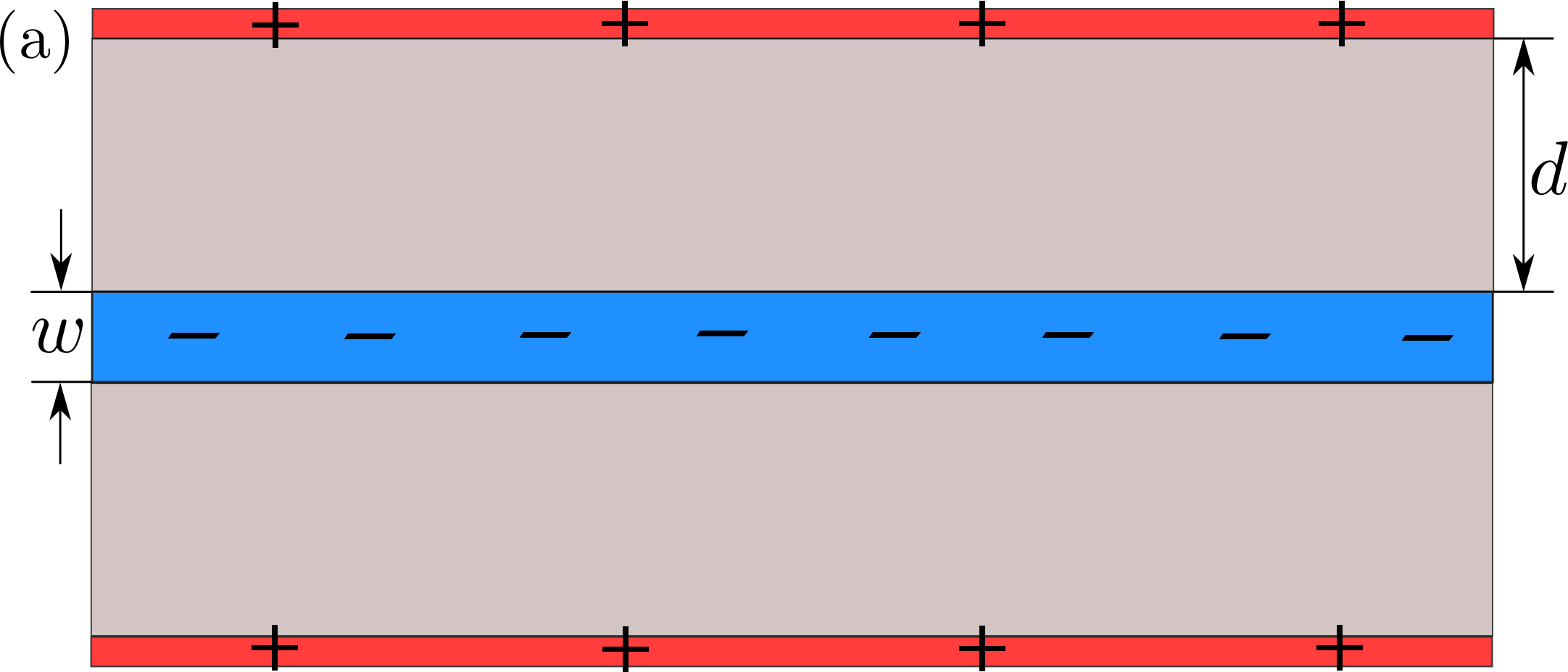

As shown in Fig. , each doping layer consists of a narrow (typical width of 3 nm) GaAs quantum well, which is doped in the middle by a -layer of Si donors with a typical concentration cm-2 and surrounded by AlAs layers with a typical width of 2 nm. The doping layer shown in Fig. is a special case of a short-period GaAs/AlAs superlattice (SPSL), suggested by Baba[35] and later implemented by Friedland.[36] Following Refs. [6], [7], and [36] we use this abbreviation for the doping scheme shown in Fig. . To our knowledge, a structure shown in Fig. 1 was first realized in the early 2000s,[37, 38] although single heterointerfaces with one such doping layer appeared much earlier.[39, 40]
The SPSL-doping scheme augments the advantage of weak RI scattering of the 2DEG electrons. In AlAs/GaAs heterostructures with thick layers, the X-minima in AlAs are higher in energy than the -minimum in GaAs. However, for thin layers size quantization plays an important role. In our SPSL-doping layers, the much lighter effective mass in GaAs produces a much larger size quantization energy than in AlAs, raising the -minimum in GaAs above the X-minima in AlAs.[41, 42] Thus, all donated electrons which are not transferred to the 2DEG (excess electrons) are stored in the AlAs side wells. Each excess electron pairs with a donor in a compact dipole atom, so that their low-temperature parallel-to-2DEG conductance is negligible. Furthermore, excess electrons choose donors which minimize their energy; this leads to significant correlations in the positions of charged donors[43, 44] and thus to a dramatic reduction of RI scattering. In what follows, we call this redistribution of electrons excess electron screening (EES) and describe it by the screening radius . EES is different from the conventional screening by the 2DEG which is described in the paper by the Thomas Fermi (TF) screening radius and exists on top of the EES. As we show, EES also reduces the BI potential.
In the first part of this paper we study scattering by the charged donors in the SPSL-doping layers. We begin with the calculation of the binding energy of a dipole atom and show that the electron localization length in the middle of the AlAs layers is 2.7 nm, several times smaller than the average distance between the donors. This means that the excess electrons are indeed localized and at low temperature their parallel-to-2DEG conductance is negligible. Localization of the excess electrons also allows us to treat the doping layer as a lightly doped 2D semiconductor and to use the classical theory of its ground state[45, 43] to study the EES. We then calculate and limited by a single doping layer containing donors with concentration and excess electrons with concentration , where is what we call the donor filling fraction. In the device shown in Fig. 1(a), neutrality requires that and can be varied by changing . In addition, some electrons can be lost to the device surface (not shown) and can be different even when is the same. Thus, for our analysis we treat as an independent variable.
We find that and grow very fast with and exceed and in the range . In this range we find
| (3) | |||
| (4) |
where is the Fermi wavenumber of the 2DEG and is the distance between the center of the quantum well and the doping layers.
Eqs. (3) and (4) are valid only if they predict mobilities larger than the standard values in the presence of donors and no excess electrons (),[46, 47, 48]
| (5) | |||
| (6) |
Because the doping layers in real samples likely have different , for the estimates below we use Eqs. (3) and (4) for a single layer with the smallest . Unless otherwise specified, here and below we use the reference sample parameters[49] cm-2, nm, cm2V-1s-1, and cm2V-1s-1. From Eqs. (3) and (4) we find that at , while at .[50] Since in modern heterostructures often exceeds this value (see, e.g., Ref. [5]), this result suggests that not only , but also , can be governed by BI scattering.
In the second part of the paper, we calculate and taking into account EES. We show that at EES eliminates scattering by all impurities located at distances larger than from the midplane of the 2DEG’s quantum well. We assume BI concentrations and in the AlxGa1-xAs barriers and GaAs quantum well, respectively, and arrive at the linear equations
| (7) | |||
| (8) |
with coefficients and which we calculate. As a result, Eqs. (7) and (8) allow one to estimate and from measured and . We find[49] cm-3, cm-3. These estimates suggest that is dominated by BI in the AlxGa1-xAs barriers, due to their larger concentration, and therefore should benefit from the purification of the Al source.[8, 51]
The plan of this paper is as follows. In Sec. II we study the quantum mechanics of an isolated compact dipole atom in the doping layer. We compute the binding energy of an electron in a compact dipole atom and show that its localization length in the plane of the layer is small enough to proceed classically. In Sec. III we study the screening of fluctuations of the donor concentration by EES and compute and [Eqs. (3) and (4)]. In Sec. IV we compute and [Eqs. (7) and (8)], taking into account EES of the BI and derive simple analytical formulas for , , , and . In Sec. V we examine the possible suppression of EES by spreading of the -layer of Si donors in the GaAs well and by roughness of the AlAs/GaAs and AlAs/AlxGa1-xAs interfaces. In Sec. VI we comment on the possible relation between the RI potential and the measured gap of the fractional quantum Hall effect at filling factor 5/2. We conclude in Sec. VII with a summary of our results and possible avenues for further improvement of GaAs/AlxGa1-xAs heterostructures.
II Localization of electrons in the doping layers
A remarkable feature of the SPSL-doping scheme is that the excess electrons in the AlAs layers are able to reduce the random potential of donors in the GaAs layer but their parallel-to-2DEG conductance is negligible. As stated above, the main reasons for this are the proximity of the electrons to the donors and the large effective electron mass in AlAs. In this section we justify this claim, showing that excess electrons, while residing in AlAs, are strongly bound to donors in GaAs.

An illustration of an electron bound state is shown in Fig. 2. Each excess electron resides in the middle of the AlAs layer of thickness and is bound to a donor in GaAs at a distance away with the localization length in the plane. The -axis is perpendicular to the AlAs/GaAs interface and the origin is centered above the donor at the midpoint of the AlAs layer. The AlAs/GaAs and AlAs/AlxGa1-xAs interfaces are treated as infinite barriers so that the electrons are completely confined to the AlAs layer. This means that there are two competing energy scales: the separation between the first and the second subbands of the AlAs layer and the Coulomb binding energy . Below we show that for reference sample parameters nm and nm. This allows us to think that electrons are bound in the plane at by an effective 2D potential
| (9) |
obtained by averaging the Coulomb attraction of the donor over the ground state wave function . Here and is the effective dielectric constant. Because the dielectric constants of GaAs () and AlAs () are relatively close, we use . (Here and below we do not discriminate between the dielectric constants of GaAs and AlxGa1-xAs for the relevant .) The corresponding Schrödinger equation is then given by
| (10) |
where is the electron’s effective mass in the plane. To find we use a variational approach with the trial wave function
| (11) |
where is the variational parameter which minimizes .

The results of the variational calculation and as a function of are given in Fig. 3, where is the in-plane effective Bohr radius and . Using for AlAs, we find nm and meV near the -point minima.[52] With nm, we then estimate the electron binding energy meV.
Above we have assumed that , allowing us to average the potential over the fast motion along -direction and treat an electron as two-dimensional. To justify this assumption we estimate the inter-subband separation . The electronic spectrum near the -point minima in AlAs is anisotropic and .[52] We find that indeed eV .
The localization length of the electron in an isolated dipole atom in the plane is given by
| (12) |
which yields nm. For cm-2, we find which should be compared to the critical value of below which electrons are localized and transport is activated.
We can estimate using the data for a Si MOSFET doped by sodium at the SiO2 side of the interface.[53] These sodium atoms donate electrons which reside on the silicon side of the interface. Such MOSFET is therefore similar to the SPSL-doping layer in which a sodium ion in SiO2 assumes the role of Si in GaAs. The activation energy of the electron conductivity along the interface as a function of the surface concentration of sodium was investigated in Ref. [53]. At small , meV, in agreement with theoretical predictions for the binding energy of an isolated donor. With increasing , decreases and extrapolation to large shows that it vanishes at cm-2. Using Eq. (12) with the binding energy of an isolated donor (24 meV) and the in-plane effective electron mass ( ) we find the localization length of the electron bound to an isolated sodium ion nm and conclude that in Si MOSFET localization sets in at . Since our estimate of for SPSL-doping layer is smaller than this value, excess electrons should be localized and their hopping conductivity at low should be much smaller than (and activated).[54] Measurements of the conductivity of SPSL-doping layers have shown that it is indeed activated.[55, 56]
III Scattering by remote donors
Since excess electrons in the AlAs layers and donors in the GaAs layer form compact dipole atoms, scattering from these dipoles can be ignored. However, localized electrons can still choose among host donors, minimizing the total energy of the system. As a result, the ionized donors are screened by the electrons, so that the correlator of the random potential energy is reduced ( is a vector in the plane). The Fourier image of the potential correlation function and the Fourier image of the correlator of ionized donor concentration fluctuations can be related as
| (13) |
and so the screening of the potential can be understood as originating from the correlations of the ionized donors. If donors of concentration are charged and uncorrelated, in Eq. (13). At small when the concentration of ionized donors is still approximately , screening by the excess electrons reduces (and thus ) by the factor . Accounting for the additional factor from the images of the donors in the 2DEG, can be written as
| (14) |
where we have used the condition , valid for the important wave numbers and not too small (see below).
Since we can treat the 2DEG as if it were confined to an infinitely thin plane located at the center of the quantum well. The contributions of RI scattering to the mobility and quantum mobility can then be calculated using Born approximation as
| (15) | |||
| (16) |
where is the transferred momentum, is the angle between the initial electron wave vector k and the final wave vector , is the inverse Thomas-Fermi screening radius of the 2DEG, and nm is the effective Bohr radius in GaAs.
The main contribution to the integrals in Eqs. (15) and (16) comes from . For such , (since ). Changing the integration variable to , and extending the upper bound of integration to (since ), we find
| (17) | |||
| (18) |
In Eqs. (15), (16), (17), and (18) the random fluctuations of the RI potential are screened twice: once by EES and once by 2DEG screening. In the absence of EES (), a single layer of donors with concentration is characterized by and one arrives at Eqs. (5) and (6) with the well-known ratio .
We now return to Eq. (14) and calculate for . Since only a small concentration of excess electrons remain in the AlAs barriers, they only occupy the lowest energy states. Such states are provided by rare pairs of anomalously close donors, separated by distance (see such a pair in Fig. ). An electron forms a dipole with one donor while the other donor remains ionized and its attractive potential lowers the electron energy by when , . At small , one can easily calculate the chemical potential which separates the energy levels of the occupied and empty dipole atoms, and is measured from the energy of an isolated dipole atom.[45] The probability to find a second donor in a disk of radius centered around the first donor is . The average concentration of such donor pairs, i.e., the concentration of electrons, is then , where factor 1/2 eliminates double counting. Recalling that is negative, one then finds[45]
| (19) |
and
| (20) |
Unfortunately, Eqs. (19) and (20) are only valid for very small .[45, 57] As mentioned in the introduction, the mobilities likely cross over from being limited by RI scattering to being determined by BI scattering in the range . In this range, we use the results of numerical modeling of the ground state of the excess electrons on random donors and a neutralizing background.[45, 43] For we find a simple fit
| (21) |
with an accuracy of 20%. Using this with Eq.(̇14) and combining with Eqs. (17) and (18), we arrive at Eqs. (3) and (4).[58]
Our results are based on the assumption that the donors are randomly distributed in the plane of their -layer. The distribution of donors at low temperatures is a snapshot of the distribution of donors at a temperature below which the diffusion of donors stops. At this temperature dipole atoms are ionized and donors separated by a distance interact with the Coulomb repulsion energy . If , the probability to find such a pair of donors is reduced by the Boltzmann factor . For the important pairs, , and using Eq. (19) we find that this effect is relevant only at , where EES plays little role. Therefore, Eqs. (3) and (4) are robust against this effect for experimentally relevant .
We have also assumed that the system of excess electrons is close to its ground state at low temperatures. Although these electrons are localized, the rate of electron hops from a dipole atom to the nearest empty donor has a large prefactor s-1 related to the emission of phonons. For cm-2 the exponential factor is resulting in s-1, much larger than the typical rate of cooling of the sample.
Our Eq. (3) for can be compared with Ref. [43] which numerically studied the screening of the RI potential by excess donors in GaAs/AlxGa1-xAs heterostructures with a conventional -doping in AlxGa1-xAs at nm (only the equilibrium theory of Ref. [43] is relevant here).[59] In the important range of filling fractions if we use the parameters of Ref. [43] our agrees with its Fig. 4(a). Ref. [43] did not study or BI scattering.
As we saw above, in modern heterostructures both and are larger than and at . However, the remote donors can become important for the quantum mobility if one succeeds to substantially reduce BI scattering. We thus would like to estimate and at , i.e., when almost all of the donors form neutral dipole atoms and only a small fraction of donors are ionized. Ionized donors can be treated as holes which repel each other and tend to form a Wigner crystal.[45, 44] If such a crystal were ideal, it would not scatter electrons. However, due to the discreteness of the random positions of donors, holes have to move from their ideal position to the nearest neighbor donor. Each such move effectively creates a dipole with the arm randomly oriented in the plane. The number of such dipoles in the relevant square of size is and because of their random orientation the amplitude of potential fluctuations created by them in the 2DEG can be estimated as . A more accurate estimate of the dipole scattering gives,
| (22) | |||
| (23) |
Note, that our results for disagree with Ref. [43], which arrived at a much faster growth of near . This is because the authors only considered macroscopic fluctuations of the donor concentration and ignored fluctuations in the position of the nearest neighbors mentioned above.
IV Scattering by background impurities
In this section we consider scattering by background impurities in SPSL-doped heterostructures taking into account EES. We begin with and calculated in the Born approximation as
| (24) | |||
| (25) |
where is the BI scattering potential.
In this section as everywhere above we assume that the 2DEG occupies the first subband only. Then the square of the wave function is well concentrated in the range near the midplane of the quantum well. If the BI are uniformly distributed with a concentration , then in the absence of EES, the scattering potential can be written as
| (26) |
It is easy to see that with such a Eq. (25) diverges logarithmically. This divergence results from scattering from an infinite number of distant impurities. (These impurities scatter at small angles so that they do not affect transport, and remains finite.) In order to truncate this divergence, one must either consider a sample with finite thickness, or use multiple scattering theory that goes beyond the Born approximation.[60, 47]
Let us now show that EES truncates the divergence even stronger. We assume that so that EES is already so strong that its screening radius , i.e. the doping layer screens a static potential as if it were a metal. This means that at , and are independent of . Let us consider an impurity at a distance from the midplane of the 2DEG, as shown in Fig. 4.

When the impurity is located between the 2DEG and the doping layer, the doping layer creates an oppositely charged image of the impurity at the distance which reduces its potential. When , the image is far from the 2DEG and its effect is small. However, when becomes close to as shown in Fig. 4 the impurity forms a compact dipole with its image whose potential in the 2DEG practically does not scatter. Thus, the scattering off of impurities located at distances larger than a critical distance becomes negligible. We can estimate by solving the equation
| (27) |
which gives . Here we use the squares of the potentials as they lead to scattering. Furthermore, we can ignore the impurities at , as the doping layer acts as a Faraday cage which screens these impurities.[61] Thus we need to consider only the impurities within the finite distance .
Now let us make our model more general and assume that the BI concentrations outside and inside the well are and , respectively. Then we can write the linear Eqs. (7) and (8) for the mobilities and with coefficients , , , and which are estimated below.
Let us first concentrate on and related to the impurities in the AlxGa1-xAs barriers. Due to EES, only the impurities of the layer contribute to scattering. Because , for the purpose of estimates we can apply Eqs. (5) and (6) to a thin layer of impurities between and with concentration , and sum the contributions of these layers arriving at
| (28) | |||
| (29) |
where we multiplied by 2 as these impurities lie on both sides of the 2DEG. We find[62]
| (30) | |||
| (31) |
Let us switch to and which are determined by impurities in the GaAs well. Here, in order to get a very rough estimates we do not discriminate between the two smallest spatial scales, the screening radius of 2DEG nm, and the “half width of electron layer” nm. Then we can write
| (32) | |||
| (33) |
where we took into account that and replaced by when integrating from to .
Using the reference sample parameters,[49], and expressing the mobilities in units cm2V-1s-1 and and in units of cm-3, we find that Eqs. (30), (31), (32), (33) give , , and . In the Appendix we develop a quantitative theory of BI scattering which confirms the estimates , and leads to slightly larger and .
Now one can easily calculate and from and solving Eqs. (7) and (8). For example, if cm2V-1s-1 and cm2V-1s-1, at we can subtract the contribution of and from and and find cm2V-1s-1 and cm2V-1s-1. They correspond to cm-3 and cm-3. In this case AlxGa1-xAs accounts for nearly of , while it accounts for only of . This large sensitivity to the AlxGa1-xAs impurities implies that for improvements one should focus not only on the Ga purity,[9] but also on the Al purity as well, particularly if one is interested in high .
Previous work[60] has shown that the ratio without EES in single heterojunction devices is . As EES reduces BI scattering, one might expect that this ratio would decrease. Yet in the above discussion, we have shown that the ratio can be as large as 18. This large number is a result of allowing and to be different, while Ref. [60] assumed that . The large ratio compensates the reduction in BI scattering by EES. If we assume that , then it follows from Eqs. (7) and (8) with , , and that EES reduces the ratio to .
Let us now consider a heterostructure in which the bottom doping layer is removed to allow tuning of the electron concentration in the 2DEG by a back gate placed at a distance nm below the 2DEG.[33, 63] In this case we expect the scattering from the impurities below the 2DEG to increase as distant impurities, which were previously screened by the excess electrons, now contribute to scattering.
The gate also produces images of background impurities which screen their static potential (see Fig. 4). Therefore, we can modify the parameter by replacing the EES screening length by the gate screening length for the bottom layer and write
| (34) |
For the reference sample parameters[49] and nm we find . This finding seems to be in qualitative agreement with experiments, which reported higher in heterostructures with two SPSL doping layers[31, 32] than in a gated heterostructure[33] of the same and tuned to the same . Note, however, that the difference in could also originate from other factors, such as different or .
Above we have assumed that the Born approximation is valid everywhere and that the logarithmic divergence is truncated by the EES of impurities. In principle, one may go beyond the Born approximation and use a self-consistent multiple scattering theory to truncate logarithmic divergence,47,60 which introduces a truncation length on the order of . For modern samples, cm-3 and the distance mm, which is significantly larger than either or , so that there is no need to use the self-consistent multiple scattering theory.
V Additional disorder in
doping layers
So far we have considered only two sources of disorder, namely, the random location of donors in a single layer in the middle of the GaAs doping well and the random three-dimensional distribution of impurities with concentrations and in the AlxGa1-xAs and the GaAs, respectively. In this idealized model, the screening radius decreases very fast with , making quickly approach and exceed .
In this section we discuss three additional sources of disorder in the doping layer, which can reduce the density of states of excess electrons, increasing their screening radius and, thus, suppressing EES. Therefore, our Eqs. (3), (4) and Eqs. (7), (8) are the best mobilities achievable in the SPSL-doped structures.
We start from the possible spreading of the Si donors over several layers of the GaAs well. The variations in the distance between donors and the middle plane of the AlAs layer leads to variations in the binding energy of dipole atoms, reducing the density of states of the excess electrons. Assuming that , where nm is the lattice constant, and using Fig. 3 we can estimate the correction to the binding energy meV. Since this correction is smaller than the typical Coulomb width of the dipole density of states meV, it should only lead to an increase of the screening radius by a relatively small fraction . If, on the other hand, Si donors are spread over larger , the RI-limited mobilities might degrade.
Another source of disorder is the roughness of AlAs/GaAs and AlAs/AlxGa1-xAs interfaces.[64, 65, 66] If we assume that these interfaces are covered by random islands of height and radius larger than the localization length , but smaller than the distance between donors, the dispersion of the first subband quantization energies of the excess electrons can be estimated as
| (35) |
If we assume that the density of states of dipole atoms with energy is dominated by roughness and has a Gaussian shape , then we can find the Fermi energy and arrive at the estimate of the screening radius for small
| (36) |
Comparing Eqs. (21) and (36), we find that they cross at , so that roughness only weakly perturbs the crossover between RI-limited and BI-limited for the reference sample parameters.[49] However, if BI scattering is reduced by making the AlxGa1-xAs barriers cleaner, then roughness will be the main limiting factor of at large . Since the roughness parameters are not well known, we do not attempt to make more accurate estimates.
The third source of additional disorder comes from possible autocompensation of Si donors. If a small fraction of Si atoms resides in the As sublattice, they are acceptors. A typical acceptor traps an electron from the nearest neighbor donor forming an acceptor-donor dipole with the arm of the order of in the plane. If we still use for the concentration of Si atoms and if the concentration of holes forming the Wigner crystal on top of them is larger than the concentration of acceptor-donor dipoles , these dipoles produce a minor effect on the random potential. Only at do the randomly oriented acceptor-donor dipoles dominate the random potential making it -independent. If, for an estimate, we follow Ref. [67] which found , this source of disorder becomes relevant only when approaches unity and thus has minor effect on our findings.
VI Quantum Hall effect at
In this section we would like to comment on the puzzle of the experimentally obtained gap of the quantum Hall effect at filling factor .[7, 20, 68] The observed K is considerably smaller than the theoretical value of K and we would like to see if our theory can shed the light on this issue.
If in the absence of 2DEG screening the magnitude of the long range fluctuations of the potential energy of 5/2 excitations , they should not affect as it is determined by the classical trajectories of excitations with activation over the saddle points.[69] However, when the disorder is nonlinearly screened by the 2DEG and creates large compressible islands separated by relatively narrow stripes of incompressible liquid.[70, 71] In this case, can be substantially smaller than due to the following effects.[68] First, the self-energy of charged excitations created in the incompressible stripes is reduced by the proximity of the excitations to the metal-like compressible islands. Second, the tunneling through the saddle points of can now happen at smaller distances which are comparable with the size of the excitation. Here, we would like to show that at the disorder is already so weak due to EES that and thus there is no reason to expect a substantial deficit of .
Even though at the remote donors and background impurities provide equal contributions to , their effective concentrations, which determine the spatial scales of their random potentials, are different. Indeed, comparing Eqs. (4) and (6) we can find that at EES reduces to an effective concentration of randomly positioned charged donors On the other hand, the BI potential is due to impurities in the layers of width located on both sides of the 2DEG. For cm-3, the two-dimensional concentration of such impurities is cm. As a result, the spatial scale of the BI potential is larger than the scale of the RI potential.[72]
Due to their smaller spatial scale , the random fluctuations of the remote donor potential are responsible for tunneling at a saddle point. For fluctuations of the potential energy of the 5/2 excitations with charge this translates to . Thus the compressible islands of the 2DEG should be small and play marginal role. Then the sum of the two self-energies necessary to create two oppositely-charged excitations should be close to and the characteristic tunneling distance at the saddle point of should be . This distance should be compared to the size of the charge excitations ,[68] where is the magnetic length. At T, nm and is five times larger than . Thus we expect that tunneling through saddle points plays a very weak role and there should be a range of temperatures in which the transport is activated with no deficit.[69] Of course, at very low temperatures one should expect that tunneling eventually becomes important and hopping transport takes over. At , the EES is weaker so that the amplitude of the potential energy fluctuations is larger and leads to large compressible islands and narrow incompressible strips which can substantially reduce .[5]
Above we assumed that the random positions of donors is the only source of disorder. As shown in the previous section, additional sources of disorder can weaken the effects of EES and lead to the deficit of . It is therefore plausible that reduction of these sources of disorder can lead to the increase of .
VII Summary
We have studied the mobility and quantum mobility in GaAs/AlxGa1-xAs heterostructures with SPSL-doping (see Fig. 1). We showed that scattering by both remote donors and charged background impurities is strongly reduced due to screening of their random potentials by excess electrons. To evaluate the strength of this screening, we considered a dipole atom formed by a donor and an excess electron in the SPSL layer and showed that excess electrons are localized and have negligible parallel-to-2DEG conductance. On the other hand, excess electrons strongly screen the random potential of the donors. We calculated the screening radius of the excess electrons and used it to calculate the remote donor-limited mobilities and [Eqs. (3) and (4)]. Our estimates show that there is a characteristic filling fraction of excess electrons beyond which not only but also exceeds the background impurity-limited mobilities and , respectively. Furthermore, the screening by excess electrons is so strong that and are determined only by impurities which are located within a distance from the midplane of the 2DEG. Our calculations of and as linear functions of the concentrations of impurities in AlxGa1-xAs and in GaAs [Eqs. (7) and (8)] provide a way to estimate these concentrations if and are known. We generalized our results for background impurity scattering to backgated heterostructures, in which the bottom doping layer is removed, and found that in these heterostructures should be roughly twice smaller than in heterostructures with two doping layers. We discussed additional disorder in the doping layers due to the spreading of the -layer of donors in the GaAs doping well and due to roughness of the AlAs/GaAs and AlAs/AlxGa1-xAs intefaces.
In conclusion, we would like to summarize possible avenues for improvement of the quantum mobility in modern GaAs/AlxGa1-xAs heterostructures. To increase , one should ensure that in both doping layers and, if necessary, find ways to minimize the spreading of donors and the roughness of the AlAs/GaAs and AlAs/AlxGa1-xAs interfaces. To increase , one should find a way to make the AlxGa1-xAs barriers cleaner, as the impurities in these layers are what limits .
Acknowledgements.
We are grateful to M. J. Manfra, L. N. Pfeiffer, and V. Umansky for discussions of growth and sample details, and Q. Shi, H. Fu, and X. Ying for their commenting of the manuscript and helpful discussions. M. Sammon was supported primarily by the NSF through the University of Minnesota MRSEC under Award No. DMR-1420013. M.A.Z. acknowledges support by the U.S. Department of Energy, Office of Science, Basic Energy Sciences, under Award No. ER 46640-SC0002567 and by the NSF Award No. DMR-1309578.Appendix:Quantitative Theory of Scattering by Background Impurities
We begin by deriving the screened interaction between a 2DEG in a quantum well of width and an impurity at a distance away from the center of a quantum well (). The impurity is screened by two electron gases the 2DEG inside of the quantum well and the excess electrons (EE) in the nearest doping layer a distance away from the center of the main quantum well (See Fig. ). We ignore the thickness of the doping layer (as it is small compared to ) and consider the screening by only the doping layer nearest to the impurity.
The screening of a single impurity is calculated using the random phase approximation (RPA), which amounts to writing a set of self consistent equations for the screened interactions between a charged impurity and the electrons. Here, we introduce the notation for the screened impurity interactions and for the bare impurity interactions, where the subscript can be 1 (2DEG) or 2 (EE). Screening occurs because of the electron-electron interactions , which can be 2DEG-2DEG (), EE-EE () or 2DEG-EE (). We assume that the electrons are completely confined inside the well and occupy only the first subband, so their linear density in the -direction is . Conversely, since we ignore the thickness of the doping layer, the linear density of the EE is given by . Using this notation, the RPA gives the system of equations
| (A.1) |
where are polarization functions of the electrons,
| (A.2) |
are the bare impurity-electron interactions, and
| (A.3) |
are the electron-electron interactions. Solving for , we find
| (A.4) |
The bare impurity interactions are straightforward to calculate from Eqs. (A.2) and (A.3). For we find
| (A.5) |
where
| (A.6) |
For we find
| (A.7) |
Similarly, we find for the electron-electron interactions that
| (A.8) | ||||
| (A.9) | ||||
| (A.10) |
where
| (A.11) |
For the polarization functions we use the Thomas-Fermi approximation which gives and .
Let us now examine Eq. (A.4) at different . For simplicity, we will set and assume , as small give the main contribution to . For , Eq. (A.4) with the interactions given in Eqs. (A.5)-(A.10) reduces to
| (A.12) |
so that an impurity at small is screened by the 2DEG but not by the EE. Conversely, for we find
| (A.13) |
so that at larger is suppressed by a factor . For and reference sample parameters,[49] and the impurities at play no role.
The above discussion allows us to make two assumptions that substantially simplify the calculations. First, we ignore EES for the impurities in the GaAs well (). Second, we ignore the impurities in the AlxGa1-xAs beyond the doping layer54 (). Under these assumptions, and can be calculated using the Born approximation according to Eqs. (24) and (25). The scattering potential is given by
| (A.14) |
where
is the 3D concentration of impurities at a distance from the center of the 2DEG, () is the concentration of impurities in AlxGa1-xAs (GaAs), and is the impurity-electron interaction with EES defined in Eq. (A.5). Performing the integration in Eq. (A.14) yields
| (A.15) |
where
| (A.16) |
and
| (A.17) |
are the form factors[66] for AlxGa1-xAs and GaAs respectively, while
| (A.18) |
and
| (A.19) |
are the dielectric functions with and without EES. With Eqs. (A.15)(A.19), we can find the coefficients , , , and in Eqs. (7) and (8). Using the reference sample parameters[49] we find , , , and .
References
- [1] H. Stormer, R. Dingle, A. Gossard, W. Wiegmann, and M. Sturge, Solid State Commun. 29, 705 (1979).
- [2] L. Pfeiffer, K. W. West, H. L. Stormer, and K. W. Baldwin, Appl. Phys. Lett. 55, 1888 (1989).
- [3] V. Umansky, R. de Picciotto, and M. Heiblum, Appl. Phys. Lett. 71, 683 (1997).
- [4] L. Pfeiffer and K. W. West, Physica E 20, 57 (2003).
- [5] V. Umansky, M. Heiblum, Y. Levinson, J. Smet, J. Nübler, and M. Dolev, J. Cryst. Growth 311, 1658 (2009).
- [6] V. Umansky and M. Heiblum, in Molecular Beam Epitaxy (Elsevier, 2013), pp. 121–137.
- [7] M. J. Manfra, Annu. Rev. Condens. Matter Phys. 5, 347 (2014).
- [8] C. Reichl, J. Chen, S. Baer, C. Rössler, T. Ihn, K. Ensslin, W. Dietsche, and W. Wegscheider, New J. Phys. 16, 023014 (2014).
- [9] G. C. Gardner, S. Fallahi, J. D. Watson, and M. J. Manfra, J. Cryst. Growth 441, 71 (2016).
- [10] D. C. Tsui, H. L. Stormer, and A. C. Gossard, Phys. Rev. Lett. 48, 1559 (1982).
- [11] R. Willett, J. P. Eisenstein, H. L. Störmer, D. C. Tsui, A. C. Gossard, and J. H. English, Phys. Rev. Lett. 59, 1776 (1987).
- [12] A. A. Koulakov, M. M. Fogler, and B. I. Shklovskii, Phys. Rev. Lett. 76, 499 (1996).
- [13] M. P. Lilly, K. B. Cooper, J. P. Eisenstein, L. N. Pfeiffer, and K. W. West, Phys. Rev. Lett. 82, 394 (1999).
- [14] R. R. Du, D. C. Tsui, H. L. Stormer, L. N. Pfeiffer, K. W. Baldwin, and K. W. West, Solid State Commun. 109, 389 (1999).
- [15] J. P. Eisenstein and A. H. MacDonald, Nature (London) 432, 691 (2004).
- [16] M. A. Zudov, R. R. Du, J. A. Simmons, and J. L. Reno, Phys. Rev. B 64, 201311(R) (2001a).
- [17] P. D. Ye, L. W. Engel, D. C. Tsui, J. A. Simmons, J. R. Wendt, G. A. Vawter, and J. L. Reno, Appl. Phys. Lett. 79, 2193 (2001).
- [18] R. G. Mani, J. H. Smet, K. von Klitzing, V. Narayanamurti, W. B. Johnson, and V. Umansky, Nature (London) 420, 646 (2002).
- [19] M. A. Zudov, R. R. Du, L. N. Pfeiffer, and K. W. West, Phys. Rev. Lett. 90, 046807 (2003).
- [20] J. Nuebler, V. Umansky, R. Morf, M. Heiblum, K. von Klitzing, and J. Smet, Phys. Rev. B 81, 035316 (2010).
- [21] N. Samkharadze, J. D. Watson, G. Gardner, M. J. Manfra, L. N. Pfeiffer, K. W. West, and G. A. Csáthy, Phys. Rev. B 84, 121305 (2011).
- [22] W. Pan, K. W. Baldwin, K. W. West, L. N. Pfeiffer, and D. C. Tsui, Phys. Rev. B 84, 161307 (2011).
- [23] G. Gamez and K. Muraki, Phys. Rev. B 88, 075308 (2013).
- [24] N. Deng, G. C. Gardner, S. Mondal, E. Kleinbaum, M. J. Manfra, and G. A. Csáthy, Phys. Rev. Lett. 112, 116804 (2014).
- [25] Q. Shi, M. A. Zudov, J. D. Watson, G. C. Gardner, and M. J. Manfra, Phys. Rev. B 93, 121404(R) (2016a).
- [26] Q. Qian, J. Nakamura, S. Fallahi, G. C. Gardner, J. D. Watson, and M. J. Manfra, Phys. Rev. B 95, 241304(R) (2017a).
- [27] S. Das Sarma and E. H. Hwang, Phys. Rev. B 88, 035439 (2013).
- [28] S. Das Sarma and E. H. Hwang, Phys. Rev. B 90, 035425 (2014).
- [29] S. Das Sarma, E. H. Hwang, S. Kodiyalam, L. N. Pfeiffer, and K. W. West, Phys. Rev. B 91, 205304 (2015).
- [30] Quantum mobility governs the amplitude of low-field quantum oscillations,[73, 16, 74, 75] which increase exponentially with .
- [31] Q. Shi, S. A. Studenikin, M. A. Zudov, K. W. Baldwin, L. N. Pfeiffer, and K. W. West, Phys. Rev. B 93, 121305(R) (2016b).
- [32] Q. Shi, M. A. Zudov, I. A. Dmitriev, K. W. Baldwin, L. N. Pfeiffer, and K. W. West, Phys. Rev. B 95, 041403(R) (2017).
- [33] Q. Qian, J. Nakamura, S. Fallahi, G. C. Gardner, J. D. Watson, S. Lüscher, J. A. Folk, G. A. Csáthy, and M. J. Manfra, Phys. Rev. B 96, 035309 (2017b).
- [34] In contrast to , precise experimental determinations of in modern samples remain rather limited. Shubnikov-de Haas measurements[33] in a gated 30 nm-wide heterostructure have found cm2V-1s-1 at cm-2. Microwave photoresistance measurements in a symmetrically SPSL-doped 30 nm-wide quantum wells with the same reported values as high as cm2V-1s-1,[32] once the electron-electron scattering contribution was subtracted.
- [35] T. Baba, T. Mizutani, and M. Ogawa, Jpn. J. of Appl. Phys. 22, L627 (1983).
- [36] K. J. Friedland, R. Hey, H. Kostial, R. Klann, and K. Ploog, Phys. Rev. Lett. 77, 4616 (1996).
- [37] K. B. Cooper, M. P. Lilly, J. P. Eisenstein, T. Jungwirth, L. N. Pfeiffer, and K. W. West, Solid State Commun. 119, 89 (2001).
- [38] J. P. Eisenstein, K. B. Cooper, L. N. Pfeiffer, and K. W. West, Phys. Rev. Lett. 88, 076801 (2002).
- [39] R. R. Du, H. L. Stormer, D. C. Tsui, L. N. Pfeiffer, and K. W. West, Phys. Rev. Lett. 70, 2944 (1993).
- [40] L. N. Pfeiffer, private communication (2018).
- [41] J. Ihm, Appl. Phys. Lett. 50, 1068 (1987).
- [42] A. R. Khisameeva, A. V. Shchepetilnikov, V. M. Muravev, S. I. Gubarev, D. D. Frolov, Y. A. Nefyodov, I. V. Kukushkin, C. Reichl, L. Tiemann, W. Dietsche, et al., Physical Review B 97, 115308 (2018).
- [43] A. L. Efros, F. G. Pikus, and G. G. Samsonidze, Phys. Rev. B 41, 8295 (1990).
- [44] R. Grill and G. H. Döhler, Phys. Rev. B 59, 10769 (1999).
- [45] M. S. Bello, E. I. Levin, B. I. Shklovskii, and A. L. Efros, Zh. Eksp. Teor. Fiz, 80, 1596 (1981), [Sov. Phys. JETP 53, 822 (1981)].
- [46] P. J. Price, J. Vac. Sci. Tech. 19, 599 (1981).
- [47] A. Gold, Phys. Rev. B 38, 10798 (1988).
- [48] I. A. Dmitriev, A. D. Mirlin, D. G. Polyakov, and M. A. Zudov, Rev. Mod. Phys. 84, 1709 (2012).
- [49] We use the following reference sample parameters: cm-2, cm2V-1s-1, cm2V-1s-1,[34] nm, nm, cm-2, nm, and nm. Samples with similar parameters are given in Refs. [7] and [31].
- [50] The sample described in Fig. 7 of Ref. [7] seems to correspond to .
- [51] Yoon Jang Chung, K. W. Baldwin, K. W. West, M. Shayegan, and L. Pfeiffer, Phys. Rev. Materials 2, 034006 (2018).
- [52] I. Vurgaftman, J. R. Meyer, and L. R. Ram-Mohan, J. Appl. Phys. 89, 5815 (2001).
- [53] A. B. Fowler and A. Hartstein, Philos. Mag. B 42, 949 (1980).
- [54] At small enough , when the density of states of the SPSL structure is small, localization can be achieved even at .
- [55] S. I. Dorozhkin, D. V. Sychev, and A. A. Kapustin, J. Appl. Phys. 116, 203702 (2014).
- [56] S. I. Dorozhkin, V. Umansky, K. von Klitzing, and J. H. Smet, JETP Lett. 107, 61 (2018).
- [57] The reason is that at the correction to Eq. (19) from the long-range potential fluctuations becomes substantial.
- [58] Actually, in Eq. (14) the concentration of randomly positioned charged donors is less than .[29] Indeed, only donors remain charged and their spacial distribution is correlated because the compact pairs of charged donors with have been eliminated. For small this results in the effective concentration of random charged donors further reduced by .[29] This would result in an additional factor in Eqs. (3) and (4), but at small this factor is less important than .
- [59] Ref. [29] uses a nonequilibrium theory of the donor correlations, distinct from our equilibrium theory.
- [60] S. J. MacLeod, K. Chan, T. P. Martin, A. R. Hamilton, A. See, A. P. Micolich, M. Aagesen, and P. E. Lindelof, Phys. Rev. B 80, 035310 (2009).
- [61] For these impurities the scattering potential is reduced by the factor at . Strictly speaking the logarithmic divergence of exists even in this case. However, it is substantial only for the sample thickness which is unrealistically large and so we can safely ignore the impurities located behind the doping layers.
- [62] This result assumes in contrast to the one[48] for .
- [63] M. A. Zudov, I. A. Dmitriev, B. Friess, Q. Shi, V. Umansky, K. Von Klitzing, and J. Smet, Phys. Rev. B 96, 121301 (2017).
- [64] H. Sakaki, T. Noda, K. Hirakawa, M. Tanaka, and T. Matsusue, Appl. Phys. Lett. 51, 1934 (1987).
- [65] H. Fu, K. V. Reich, and B. I. Shklovskii, Phys. Rev. B 93, 235312 (2016).
- [66] A. Gold, Phys. Rev. B 35, 723 (1987).
- [67] S. S. Bose, B. Lee, M. H. Kim, G. E. Stillman, and W. I. Wang, J. Appl. Phys. 63, 743 (1988).
- [68] N. d’Ambrumenil, B. I. Halperin, and R. H. Morf, Phys. Rev. Lett. 106, 126804 (2011).
- [69] D. G. Polyakov and B. I. Shklovskii, Phys. Rev. Letters 74, 150 (1995).
- [70] A. L. Efros, Solid State Commun. 67, 1019 (1988).
- [71] F. G. Pikus and A. L. Efros, Phys. Rev. B 47, 16395 (1993).
- [72] While at , the BI and RI contribute equally to . The reason for this is that , where is the scattering cross-section. The cross section decays quickly with , so that the larger it is, the smaller the range of that contributes to scattering.
- [73] L. Shubnikov and W. de Haas, Leiden Commun. 207a (1930).
- [74] M. A. Zudov, I. V. Ponomarev, A. L. Efros, R. R. Du, J. A. Simmons, and J. L. Reno, Phys. Rev. Lett. 86, 3614 (2001b).
- [75] C. L. Yang, J. Zhang, R. R. Du, J. A. Simmons, and J. L. Reno, Phys. Rev. Lett. 89, 076801 (2002).