Metallic nanolayers – a sub-visible wonderland of optical properties
Abstract
It was predicted long ago that ultra-thin metallic films must exhibit unusual optical properties for radiation frequencies from to infrared domain. A film would remain highly reflective even when it is orders of magnitude thinner than a skin depth at any frequency. Only when it is a few nanometers thick (depending on material but not on the frequency), its reflectivity and transmittivity get equal, while its absorption peaks at 50%. It has been confirmed experimentally and new directions and applications were proposed. We review the EM theory of the phenomenon and recent developments in the field, and present some new results. 2018 Optical Society of America
OCIS codes: 310.6860 Thin films, optical properties, 260.0260 Physical optics, 040.3060 Infrared
Introduction
The optics of metals is a prominent part of optical physics and related technologies, in particular EM-devices from radio to microwave to infrared wavelengths; we will call it () domain. Of utmost importance to optics is the capability of polished metal surface to serve as an almost ideal mirror, including visible domain. This quality was well known to humankind from ladies mirrors in ancient Egypt, to the legend of Archimedes’ use of soldiers shields to focus sunlight into the enemy’s ship sails, to radars, telescopes, and other modern reflectors.
Due to very high conductivity of metals, , the major properties of metallic mirrors in dielectric environment are: (1) their reflectivity is very close to at any frequency within domain and their absorption, , is respectively tremendously low, (2) the electrical field at the reflecting boundary nearly vanishes (i. e. the reflected EM-wave is almost of the same amplitude, but of the opposite phase, forming thus a standing wave with a node at the surface); (3) yet since the conductivity is still finite, the exponentially decaying field penetrates into the metal to a very shallow ”skin depth”, , which is orders of magnitude lower than the wavelength of light in free space, , i. e. . The phenomenon has been first experimentally explored by Hagen and Rubens [1], and electromagnetic theory for semi-infinite metallic layers was developed by Drude [2] more than a century ago.
Modern day applications and related physics call for the use of very thin metallic films, , or even – down to a few atomic layers – and at the same time offer capability of fabricating such thin films. (The technique of making ”gold leaves” less than thick was known to humans from the ancient times, and used in art and architecture [3].) The issue arises then how thin must be such a layer to have its reflectivity in substantially reduced and its transmittivity, , increased. A characteristic thickness would be say such that . A common perception is that it happens when the layer’s thickness reaches skin depth, , and that the absorption gets even lower.
A fact of the matter is that such a perception is wrong by orders of magnitude. As was shown in [4], the reflectivity is drastically reduced only at amazingly small thickness, , orders of magnitude lower than the skin depth, down to a nanometer for metals, corresponding actually to a small number of atomic layers. Regardless of a specific metals, at such point , and the absorption reaches its maximum, , very large as compared to that of a semi-infinite layer. (Furthermore, in counter-propagating waves, a full absorption reaches [5] at that point, and such a film becomes an ideal black-body, with .) On the other hand, easily fabricated films of the thickness , i. e. greatly thinner than a skin depth, , may remain almost fully reflective, , so they can still be used as good mirrors.
This thickness, , is essentially a new and most fundamental scale of metal optics in domain, as it is frequency-independent unlike , and relates only to electronic properties of metal, such as conductivity (Sections 2), or, under detailed consideration, - mostly the density of free electrons (Section 6). However, an amazingly simple nature of this effect greatly overlooked in general literature, is that at that thickness one attains impedance matching between the environment and metallic layer resulting in maximum absorption. In a free-space environment, the -layer’s impedance, , is exactly half of that of vacuum, , , and it does not depend even on specific metal (see details in Section 5 and 6). It would be reasonable to call an impedance-matching thickness.
The effect has by now been verified and explored both theoretically and experimentally. That research included early [6 – 9] and recent [10 – 13] millimeter wave experiments; applications to the visualization of microwave modes using thermoluminescence sensors [14 –- 16], broadband millimeter wave spectroscopy in resonators at cryogenic temperatures [17 – 19], the theoretical and experimental study of EM-properties of periodic multilayers of metallic films (photonic crystals) [20,21]; and a proposal to attain 100% EM absorption in a standing wave [5]. However, it would be not an overstatement to note that aside from those studies, this strongly pronounced and physically transparent effect remained little known to the research community in the optics of metals, making it a blind spot in the field (the choice of term ”sub-visible” here is not accidental). The theoretical and experimental tools required for its exploration are not overly sophisticated and were available for almost a century, yet even mentioning of it is lacking not only from classical texts on electrodynamics, but also from recent reviews on the subject. The objective of this paper is to make a consistent review of the major features of the optical properties of ultra-thin metallic films (including new results), their underlying physics, and experimental results.
A brief overview of optical properties of semi-infinite metallic layers in domain is found in Section 1. Sections 2 and 3 are on the electrodynamics and optical properties of the layers of finite thickness, and Section 4 - on electrical currents. Section 5 treats the problem in terms of impedance theory, in particular for arbitrary input/output environment. Section 6 addresses the issue of how the size dependent conductivity affects the optical properties of the layers, and Section 7 - experimental results and consideration for future experiments. Section 8 is on the wave interference at metallic films resulting in 100% absorption (blackbody effect); and Section 9 briefly discusses potential applications and outlook.
1. Semi-infinite metallic layers
Major EM properties of semi-infinite (or sufficiently thick, ) metallic layers, found in any ”old goldies” texts, such as e. g. [22-26], can be represented by a succinct formula for the reflectivity, , and the absorption, , of the layer for a normal EM-wave incidence [1]:
| (1.1) |
where is a wave number, is a free-space wavelength for an -monochromatic wave, is a conductivity of the layer (we use here Gaussian units, see Appendix A, whereby ), and
| (1.2) |
is a skin depth. For metals [and other highly conductive materials, with or ], one has , so that ; this is due to large and almost purely imaginary dielectric constant of metal, (see Appendix A). As an example, for a silver layer at , (respectively, for , ). Thus the EM-properties of the system, , , and depend both on frequency of incident light and conductivity of the layer, , as expected. Much less appreciated (yet known, see e. g. [24]) fact is that the total electrical current near metallic surface, , induced by the incident wave – remains the same for any metal and wavelength, and its amplitude, , depends only on the incident amplitude as
| (1.3) |
where is the free space wave impedance (see Appendix A). A simple explanation of that is this. Due to almost full reflection of light at the surface of a semi-infinite layer and formation of standing wave in the free space with a node at the surface, an -field there almost vanishes, while the magnetic field peaks out, reaching amplitude , where is the distance from the surface. Thus we have a rare situation of an almost purely magnetic wave, although it rapidly decays inside the layer, . For a plane wave in a good metal (see details in Section 4 below), due to Amper’s law, this -field induces local currents , , see below, Eq. (2.2), so that , which results in (1.3).
It has to be noted though that the ratio is the impedance of the metal surface; a respective impedance, , must relate the current to the -field amplitude, at the surface, (see Section (2) below). and to much larger amplitude of the incident wave, , so that
| (1.4) |
Considering free space as a transmission line for a plane wave, corresponds to its short-circuiting, hence full reflection, as one would expect. Rewriting (1.4) as
| (1.5) |
| (1.6) |
we introduce a new, frequency independent characteristic length scale of a layer, , which will become one of the major ”characters” of the story for very thin layers. It is a characteristic scale at which, is one presumes that the layer conductively, remains the same as the bulk conductivity , the reflection would gets significantly reduced, and the transition respectively increased. For good metals, this new scale has atomic size (and even less than that) and is not only many orders of magnitude smaller than the wavelength of incident light, but also of the skin depth. In real layers, however, the conductivity, depends of the layer thickness, , and gets greatly reduced as (due to the fact the mean free path of electrons, , with , gets ”clipped” by the walls). see Section 6 below. This ”clipping” results in the formation of another scale, , which will finally determine the depth, , at which the layer will universally to the point where the reflectivity, , will be exactly equal to the transmittivity, , with , and absorption will peak at , see Fig. 1 for the case of silver layer and normal accidence.

This new scale is of the order of , and defined as , where , is the bulk mean free path of electrons, and is the number density of free electrons (for details, see Section 6).
The conductivity in domain remains essentially the same as for a current [1,2], i. e. the entire phenomenon is of a (quasi)static nature. This greatly simplifies the theory of the optical properties of metal in particular thin metal films, in that domain, and makes the entire domain so special. However, at the upper-energy end of this domain, the interaction of radiation with quasi-free electrons, at least in semi-infinite layers, reaches the point where the skin depth gets smaller than the mean free path of electrons, , which results in the so called anomalous skin effect [27]. The interaction then becomes non-local: the electrons driven by the field near the surface, run away into a no-field area. For example, in the case of silver, the wavelength at which this happen is in sub-mm domain, . For shorter wavelength radiation, an absorption is increasing; however the metals mirrors still remain well-reflecting even in the visible domain. However, for thin layers (see Section 6), the onset of non-locality shifts to shorter wavelengths, since gets closer to the layer thickness ; quasi-static model of optical constants of nano-layers holds true to the mid-infrared domain. A review of the electronic properties of various metals and their related optical properties from classical Drude-Lorentz model to the quantum theory for various metals and frequencies can be found in [28 – 31].
For the higher photon energies, as e. g. in spectral domain, the quasi-free electrons can be regarded as an over-dense plasma (see also Appendix A), having now almost real yet negative dielectric constant . with the plasma wavelength found in range determined by the density of electrons. Beyond that threshold, metals can be viewed as a plain under-dense plasma, with its dielectric constant approaching that of a free space, . Further into X-ray domain, the number of free electrons undergoes large jump-like increases as photon energy increases near so called , , , and absorption edges, which are due to resonant photo-ionization of bound electrons from respective shells into conduction state [32–34]. These jumps would affect the optical constants of metal surface, and may be used for various applications, in particular for narrow-line transition radiation by electron beams traversing a multi-layer, super-lattice structure of metallic layers generating almost coherent radiation in soft [35] and hard X-ray [36] domains. In this paper we limit our consideration only to the quasi-static, i. e. spectral domain.
2. Fields in a layer of finite thickness
The optical properties of thin metal layers (both in visible and far-infrared domain) with a lot of experimental data has been reviewed in [37–40] (a relevant research has been done on absorption by small metal particles in infra-red, [41]). Some of them clearly pointed to layers ability to sustain high reflectivity at surprisingly small thickness (see e. g. [42,43]); yet a general picture of existence of universal maximum absorption and a corresponding spatial scale related only to the number density of free electrons (Section 6 here) did not seem to transpire yet. It is also interesting to note that a tremendous amount of work on the physics of superconductivity, especially on high-TC superconductivity, has been done by studying infrared and far-infrared optical properties of thin films of those materials (see e. g. review [44]), with some of them emphasizing that the spatial scale of strongly absorbing films are below the skin depth (see e. g. [45]).
This and the following Sections are to provide a basic understanding of how the ultra-thin metallic films reaches the state of maximum absorption, , and to show that this behavior is really universal. While looking for the fields and current in a (non-magnetic) layer of finite thickness, for our purposes, we consider only normal incidence, i. e. the waves propagating in the -axis normal to the layer, Fig. 1. In this section, we consider only a free space as an environment, where the layer is bounded between , and . (The results are extended to arbitrary environment in Section 5.) All the calculations in this paper are based on most simplifying assumptions, sufficient to bring up and quantitatively describe major features of the phenomenon discussed: the layer has flat surfaces, and the metal in it is homogeneous (i. e. not granulated), so that there is no scattering of light at the layer; the conduction electrons are regarded as a gas of non-interacting particles following Drude model [46], that may get scattered by ions and the surfaces of the layer. An -monochromatic wave is incident normally at the layer at the point . (For the incidence close to the normal one, the results are expected to be not much different, since the refractive index of metals is large.) The wave is linearly polarized in the -axis, both incident fields and have the same amplitude , and everywhere. We designate , and . In this case, the Eqs. (A.1) and respective wave equation e. g. for are written as
| (2.1) |
where and are free-space wavenumber and wavelength of the wave respectively. The free-space dielectric constant is , whereas inside the layer, , under a ”good metals” condition, , or , can be well approximated as purely imaginary quantity (see also Appendix A):
| (2.2) |
where a scale [4] was introduced in (1.6), and is as defined in (1.2). The incident -field of amplitude , -field of amplitude , and reflected fields of amplitude and at are respectively as
| (2.3) |
The transmitted fields behind the layer, i. e. at will be sought for as
| (2.4) |
where and are the coefficients or reflection and transmission respectively to be found from boundary conditions at the surfaces of the layer. (The solution (2.4) for the transmitted field takes into account the so called Zommerfield’s condition in the infinity (), by ruling out a back-propagating wave at .) Inside the layer the fields and are superpositions of forward (”+”) and backward (”-”) propagating waves with normalized amplitudes as
| (2.5) |
with
| (2.6) |
where is a (complex) refractive index of metal. The constants are found from boundary conditions at and for and (to be continuous at a boundary). Using (2.4), (2.5), we have at :
| (2.7) |
and at :
From these equation, the solution for is then
| (2.8) |
Using the fact that , hence , we simplify (2.8) as
| (2.9) |
For very thin layers, , we have
| (2.10) |
(for see below, (2.14)), i. e. the both counter-propagating waves, are of almost the same amplitude. Eq. (2.5) yields now for the fields inside the layer:
| (2.11) |
hence
| (2.12) |
in particular, for a semi-infinite layer, ,
| (2.13) |
In most interesting case of a thin layer, , we have
| (2.14) |
i. e. , so the electrical field is homogeneous inside the layer.
3. Reflectivity, transmittivity, and absorption
From (2.7) , hence, using (2.8)
| (3.1) |
If , we have , as expected. If , the terms tend to zero, so that
| (3.2) |
and consistently with (1.1) we have
| (3.3) |
For , similarly to (2.9), (3.1) is simplified as
| (3.4) |
In the same way, we have the transmission coefficient, :
| (3.5) |
Both of them can be further simplified for the case of very thin layer, [4]:
| (3.6) |
Translating Eqs. (3.6) for thin layers into the formulas for reflectivity, , transmittivity, , and energy losses, , we get:
| (3.7) |
Interestingly enough, (3.7) provides us with a relationship that doesn’t explicitly include any parameters of the incident field or the metal:
| (3.8) |
Notice that the first of these equations, written as is not related to the conservation of full momentum in the system; indeed that conservation should include the momentum, , transferred to the layer:
| (3.9) |
which originates a radiation pressure on the layer. In the semi-infinite layer case, , i. e. is maximal, as expected, whereas at , and finally at . However, (3.7) and (3.8) uphold the conservation of radiation energy, .
4. Electrical current in the layer
As long as the solution for electrical and magnetic fields (2.11), (2.14) are known, the electrical current in the layer is found as
| (4.1) |
For a thin layer, , the field is almost constant (2.14), so the current is also evenly distributed along the depth. The current, , in the layer is
| (4.2) |
or by using the second equation in (2.11), we have
| (4.3) |
For a very thin layer, , we have
| (4.4) |
In a semi-infinite layer, , or , we have from (4.3) (see also (1.3)):
| (4.5) |
As long as , the total current is almost the same! Furthermore, the efficient layer resistance per square cm, coincides exactly with the half-impedance of vacuum. Thus the layer almost always makes the same radiating antenna, from down to .
5. Transmission line analogy; arbitrary environment
It is instructive and revealing to describe EM wave propagation through a thin metallic layer as a transmission line problem, by using wave impedances of the line and its components. A simple impedance algebra allows for an easy generalization of our results to a system with arbitrary (i. e. not just free space) input/output environment, which may include e. g. dielectric or semiconductor substrate. At the same time if offers a plain ”electrical engineering” view of the phenomenon.
Let us start with a free space environment. Both of the impedances of the ”incident” and ”output” arms of the line is then , and in view of quasi-static nature of the problem, a layer can be regarded as a lump circuit (even for a semi-infinite layer), which in the case of is simply a resistor. Thus, for all the purposes, using (2.11) with and (4.3), the impedance of a layer of a thickness is found as , or
| (5.1) |
In the limit we have
| (5.2) |
We can also find directly from the wave solution (2.13). Indeed, for a plain wave, a wave impedance in electrodynamics is usually defined as
| (5.3) |
where subscripts refer to a respective unit system. This is still true even if the wave goes through an absorbing material, if there is no retroreflection inside it. In a semi-infinite metallic layer, the ratio remains constant, (2.13), since the wave propagate only away from the interface (see e. g. (2.5) with as follow from (2.9) with ), and thus we have which coincides with (5.2). In the limit we have for the layer impedance :
| (5.4) |
The coefficient of reflection, , of the layer, if the wave is incident from , can be evaluated by assuming that the incidence line with is loaded by the impedance formed by two elements connected in parallel: the layer, with its impedance , and the output line with its impedance , i. e.
| (5.5) |
so that a transmission line theory yields
| (5.6) |
Similarly, the coefficient of transmission is evaluated as
| (5.7) |
so that for they coincide with the respective result (3.6). Finally, the energy losses are as
| (5.8) |
which peaks () at , as expected.
The transmission line results can be readily generalized to the case whereby semi-infinite dielectric materials sandwiching the metallic layer are different. Assuming that the material of the wave incidence has a refractive index and the output one – the index , so that their respective wave impedances are with , we define ”input/out load impedance” as
| (5.9) |
and use it to generalize (5.6) and (5.7) as:
| (5.10) |
| (5.11) |
We obtain then the energy losses as
| (5.12) |
If , the results (5.9)-(5.11) coincide with (5.7) - (5.8), including the case , when they coincide with (3.7). The losses (5.12) then reach their maximum
| (5.13) |
while the reflectivity and transmittivity are as
| (5.14) |
Note that if in (5.13) , the losses greatly increase; this may happen if dielectric at the entrance is highly optically dense, as in some semiconductors, or if the output medium consists of plasma near critical frequency, when . For example, if one uses silicon (), or gallium arsenide (), both of which have refractive index , as an input medium (), and an air as an output one (), one would have highly absorbing and low reflecting layer , , and at .
Having in mind that e. g. in a free space the maximum absorption happens when the layer impedance matches exactly half of vacuum impedance, regardless of the specific material, it might be perhaps appropriate to call the entire phenomenon an impedance-match absorption.
6. Size-affected conductivity, and new fundamental thickness scale
For ultra-thin films, eq. (3.7) suggests a very simple and transparent dependence of optical properties , , and film thickness – assuming that the conductivity and the scale (2.2) are constant that don’t depend on . (The resulting scale is around or even less than one angstrom.) But at very small this is not true anymore, so that dependence has to be taken into consideration. The major parameter through which the specific conductivity of good metal is affected by the film size, , is the mean free path of electrons, , with the conductivity being proportional to [47,48]:
| (6.1) |
where and are respectively specific bulk conductivity and bulk mean free path, is number density of conduction electrons, is the electron mass, is the Fermi energy of an electron gas at a given temperature; for the most applications the temperature are less then , so is the same as for absolute zero [49], , where is the Fermi wave vector, which reduces in (6.1) to
| (6.2) |
where is the fine structure constant. The experimental and theoretical data for can be found in many publications; the latest extensive study for 20 metals using numerical calculations over the Fermi surface found in [50]. The size effect, i. e. how and depend on represents fundamental interest as well as application challenges for nano-electronics. Sufficient for our purposes here is a classical Fusch-Sondheimer model [47,48], which assumes a so called a spheric Fermi surface, whereby the major factor affecting and is electron scattering at the layer surfaces. Within that model, under the most realistic assumption that electrons scatter at the surface in a purely diffuse way, the dimensionless mean-free path of electrons and the conductivity, the layer width, is as [48]:
| (6.3) |
or in terms of exponential integral [51]
| (6.4) |
In the limit of very thick layer, , the solution (6.4) is , whereas in the limit of very thin layer, , which is of most physical interest, the solution is .

To simplify the analysis of the result (6.4), we found that for all the practical purposes, in particular in the above limits, it is interpolated with great precision within an entire range by
| (6.5) |
see the comparison of (6.4) and (6.5) at Fig. 2. A layer thickness, , where the absorptions peaks out, , according to (3.7), satisfy the condition . Thus to solve (6.5), we recall that , replace by (unknown yet) as
| (6.6) |
and define a new fundamental spatial scale, , directly related to , since :
| (6.7) |
As opposed to , it does not depend on free electron path and therefore on temperature, same as the Fermi wave vector, . (While still depends on , this dependence is logarithmically weak at .) Using this scale, we introduce now dimensionless variables
| (6.8) |
where is a ”free electron figure of merit” ( for either good metals, as e. g. for , or long mean free path of electrons, as e. g. for ), and is an inverse position of peak absorption weighted by . Eq. (6.6) is rewritten then in the form
| (6.9) |
It makes it convenient to plot and analyze figure of merit, , dimensionless peak position, . For poor conductors, we have (i. e. ), the solution of (6.9) is , or , and since , we have , as expected when , i. e. the absorption peak position coincides with that predicted by a simple theory within which , In general, to find , for a given , we need to inversely solve (6.9) for . This is greatly simplified for good metals, whereby and . Eq. (6.9) then is reduced to , and a good estimate can be obtained via fast converging iterations, whereby , and , by e. g. using or even .
Eq. (6.5) allows to generate plots of reflectivity , transmittivity , and energy losses , the thickness using (3.7) [having in mind now that for any given the parameter depends now on , via in (6.5)]. Fig. 3a, shows those plots for the example of silver film [4]. One can see that the absorption, , has a peak, (and ), at the thickness Å, as predicted by (6.9) (or simplified calculations for , see the preceding paragraph), based on the known data (see Table 1) that the characteristic length for silver is Å, and the mean free path of electrons is Å. Based on those two numbers, we also estimate the new spatial scale as Å, and the silver figure of merit as .
![[Uncaptioned image]](1803.02437v2/table_reduced.png)
As one can see from Table 1, good metals (, , , and ) have their conductivity of the same order, which is also true for their mean free path of electrons, Å, and the scales Å, and Å, resulting in Å. The theoretically calculated reflectivity , transmittivity , and absorption the thickness for a silver layer are shown in Fig. 1.
In view of the results of Section 5, it is important to evaluate how the major characteristics of thin films changed for the input/output environment different from free propagation, e. g. when , where and are the refraction coefficients of input and out media respectively. Having in mind that due to (5.13), , where is the thickness that corresponds to peak absorption, (5.13), the ratio is determined now by eq. (6.9) modified as
| (6.10) |
for good metals, , it can be further simplified as . Notice that depends only on the sum , and not on individual indices ’s, while the optical characteristics , (5.13), , and (5.14), depend on ’s separately. At that, if , we still have , and , as in free propagation. Similarly to (6.9), eq. (6.10) is readily solved numerically by fast converging iterations, starting with . For example for Aluminum at , (air+glass) we have , while at , (air+silicon), , with .
7. Experimental observation
One of recent publications on experimental measurements of the effect and observation of the peak absorption in films was the work by Andreev and co-workers [11], who studied the optical properties (, , and ) of thin aluminum film using radiation with . Their results are depicted in Fig. 3 [11], for a film deposited on a glass substrate with refractive index ; Fig. 3a is for the configuration whereby the wave is incident upon film from air, and Fig. 3b - from the substrate. (In those plots, the reflectivity is denoted by , i. e. the same as in this paper, whereas denotes transmission, i. e. corresponds to in this paper, and – absorption corresponding to here.) Theoretical plots were calculated for the film environment consisting of two different materials (air and glass), using formulas similar to (5.10)-(5.12), and the size-dependent conductivity – using equations similar to (6.5) in the limit . As one can see, the experiment shows a great qualitative agreement with the theory, which is also true for quantitative agreement at the thicknesses greater than Å (2 nm ). However the position of the maximum absorption is almost double of that predicted by the theory; the authors’ explanation of that is that at that thickness (), a thin films undergoes a structural transformation, whereby it gets granulated (which may depend very much on the way the film was prepared [37]) or even breaks up into islands, which results in much faster reduction of averaged conductivity; hence the shift of peak of absorption to a greater thickness. We also note that in strongly granulated films, the ”absorption” calculated as , could be very much due to strong scattering [37] and not due to real losses in the film.
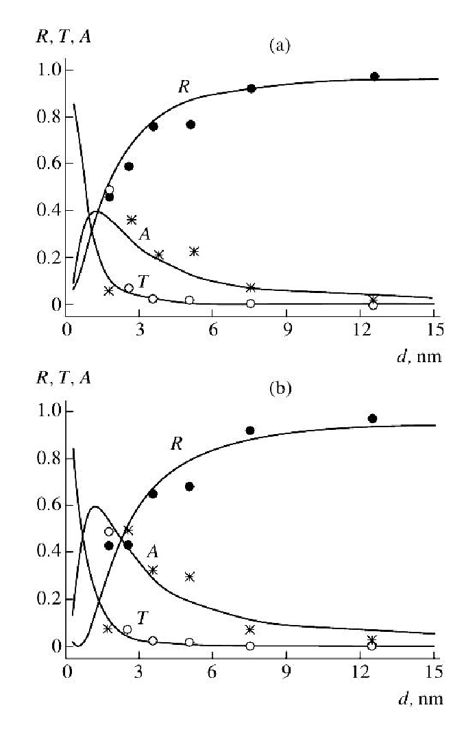
Having in mind possible future experiments to find out whether the theory based on the assumption of a homogeneous layer is still good around the peak of absorption, one might be interested to use a metal with lower intrinsic bulk conductivity and thus - greater , hence still relatively unperturbed structure with greater number of atomic layers, One can see from the Table 1, for the metals with lower bulk conductivity (, , , , and ) but roughly the same , the scale and peak position predictably increase, up to Å and Å (for ) respectively; this should make it easier to measure all the related effects in more homogenius structure.
Semi-metals such as e. g. tin, graphite, bismuth, telluride, and their chemical compounds (including most recently developed semi-metal polymers [53]) may be even more promising potential candidates for further explorations of the phenomenon considered here, for they could have much longer mean free path of electrons, and may provide an arena of almost ideal homogeneous (i. e. granulation-free) layers that can be much easier to use for more cleaner experiments. A good example is Bismuth () that has [52] (see Table 1). Having a mean free path of electrons about at it would exhibit impedance-math absorption close to 50% at the thickness near , which allows to have it as a free-standing films. At thicknesses below and low temperatures, becomes a semiconductor [54], which would make it a different and even more interesting game.
8. Free-space terminator and coherent broadband interferometry
In waveguides or transmission lines, the full absorption of incident wave is attained by a terminator whose impedance matches that of the waveguide - but not in free space. However, it was demonstrated in [5], that such ”black-body” (BB) can be realized by using a thin metal layer of exactly the thickness (which has only half of impedance of free space) in a Sagnac interferometer. It would then provide 100% absorption (hence zero reflection) for the entire spectrum of incident radiation in one position and almost full transparency in another; such a device might be of great interest to many applications. The effect is due to ideal coherence between incident and transmitted radiation for all the frequencies involved: because of tremendously low distance of propagation the phase of transmitted wave is exactly the same as that of incident wave, while the reflected wave has an opposite phase, which is true for the entire spectrum.
To realize this effect one needs waves of the same amplitude, running normally to the layer (without the layer they would form a standing wave). Since the amplitude reflection coefficient, the reflection of a straight-propagating (“+”) incident wave of the unity amplitude at will form a back-propagating wave, with the amplitude . At the same time, if a back-propagating (“-”) incident wave have exactly the same phase at the film as the “+” incident wave, its transmitted portion, will have the same phase, and , so that , and similarly, . Thus, there will be waves escaping from the film into any direction, and the energy of both waves will be fully absorbed!
In such a case, the layer is to be located in the anti-node (i. e. maximum of electric field) of the original standing wave, so one should expect the largest absorption due to largest generated electrical current. It is clear then that when the film is located at the node of the original standing wave, where the electrical field vanishes, the absorption vanishes too, as if there is no absorbing layer at all.

Such a system can be realized as a ring (Sagnac) interferometer, Fig. 4, in which an incident wave is split into two waves of equal intensity. Those are then made to propagate against each other on the path with a thin metallic film in the middle. If the film is positioned at the anti-node of the standing wave, the light energy will be fully absorbed, whereas if it coincides with a node, there will be a full reflection. For an -monochromatic wave the BB-reflection, normalized to that of the system without the BB layer, offset of the layer from the ant-node is where and . For an incident radiation with arbitrary temporal profile, with , and normalized autocorrelation function, , where brackets stand for time averaging, as (), the respective spectrum is:
| (8.1) |
If one of the output channels, e. g. channel 2, behind the film, Fig. 4, is blocked, the output signal in channel 1, , is formed then by the input 2, , that gets through the entire loop without change of sign and attenuated by the factor of , and by the input 1, , that gets reflected by thin film with the same attenuation, but with the change of sign, so that
| (8.2) |
where is a retarded time, with is a full time delay of the light to go around the full ring of the length . The normalized BB-reflection at the fixed delay is then: . Using (8.2), and having in mind that due to (8.1), , and , we have
| (8.3) |
Note that , as , and, for , we have . A typical example is a Gaussian spectrum, , with an arbitrary bandwidth centered around some frequency :
| (8.4) |
where . The total reflectivity is then
| (8.5) |
with . Fig. 5 depicts for various ratios .

With both of the output channels opened, the full output signal is similarly to (8.3), the full BB-reflection is or
| (8.6) |
In the case of the Gaussian spectrum (6) we have:
| (8.7) |
For monochromatic input, , we have . In the case of white-like noise. i. e. there is no distinct central frequency of the signal, , or simply , equations (8.5) and (8.7) are reduced to
| (8.8) |
At , we have while , i. e. double channel detection is much more sensitive to the high-frequency details of the spectrum. In general, using both reflectivities, (8.5) and (8.7), one may substantially enhance the temporal & spectral resolution, because of simultaneous auto-correlation at two different delay times, and . Fig. 5 depicts for various ratios .
9. Applications and Outlook
Having a nanometer-thick film absorbing 50% or even 100% of incident power of extremely broad spectrum may have quite a few promising applications. We will discuss a few of them, yet there is no doubt that there could be others. Besides, one can expect some interesting directions of research related to such films.
So far we discussed a coherent spectroscopy of signals with super-broad, almost white-noise spectrum. To measure such signals most of the elements of the Sagnac interferometer must be metallic, including all the mirrors, and the semi-transparent mirror should be made also the same way as the black-body element, i. e. by using again a very thin metallic layer. This is necessary to extinguish any possible resonant or frequency-sensitive effects if the mirrors are made of dielectric layers. This kind of spectroscopy would be appropriate for sub-visible domain down to mid-infrared. It is well suited for Terahertz technology; other applications may include the detection of high-frequency coherent features that may allow for detecting an information transmission in ”pseudo-white-noise” signal, and potentially, in radiation from the space that may be helpful in the detecting extraterrestrial signals, as well as in low-level signal such as primordial thermal radiation. In all these potential applications the important factor is that in contrast to regular auto-correlation techniques, whereby the auto-correlation signal at small delay times is finite, the BB-interferometry produces a zero output at , which may greatly increase its sensitivity compared to that of a regular auto-correlation. For certain applications, e. g. for primordial radiation, special care should be taken of black-body radiation of the BB-element (same as the other mirrors) by cooling it down with e. g. liquid helium.
Further modification and enhancement of the BB-interferometry, especially for narrow-band signal, may be attained by employing more than one metallic layer and using ensuing resonances. For example, for the monochromatic radiation with wavelength , if the spacing between layers with is , the system is fully transparent, if irradiated from both directions. Inversely, a reflection resonance would exist if the spacing is . In this case, the amplitude of reflection of each of the counter-propagating waves is , and transmission, . If the couple is positioned strictly at the center of the ring interferometer, the amplitude reflection for each of the waves is , and the intensity reflectivity is thus %. This is not far from total zero as with a single layer, but the system has substantial selectivity to the frequency. In thin-metal multi-layered structure [20,21] the resonant effect will be enhanced.
Another feasible application might be related to the use of layers for detecting and imaging/visualization of on radiation by covering a metallic film with thermoluminescent layer (i. e. whose luminescence strongly depends on temperature) continuing along the line of the original research [14-16] but using more advanced materials (see e. g. [55]). If such a material is preliminary irradiated by e. g. UV-radiation and then – by infrared, the spots where infrared is stronger, will be heated up enough to trigger visible thermoluminescence from such spots. The visible optical image is expected to have then very high spatial resolution, since the heat transfer along the layer would be negligible due to its extremely small thickness.
Another expected effect is related to nonlinearity of the layers slightly thinner than the peak absorption, e. g. less than . At the thicknesses corresponding to the formation of isolated ”islands” of metal, which are still close to each other, the local field due to formation of plasmons can get enhanced by orders of magnitude and due to closely packed islands induce tunnelling transitions and discharges, i. e. strongly nonlinear effects that may result in high harmonics generation.
It would be of great application interest to develop a tool of fast and efficient modulation of optical properties of ultra-thin films, especially in the vicinity of maximal absorption, by using an electro-optical effect to control behavior of free electrons in a film, as e. g. in [56].
Application-wise it would be interesting to use inexpensive ”artificial” metal-like polymers, i. e. highly conductive doped polyacetone whose electrical conductivity can be varied over the range of eleven orders of magnitude [57], polyanilin [58], and others (see review [59]. Related to that would be development of controllably produced 2D spatial modulation of the conductivity of the thin film, allowing thus opportunity to design 2D photonic nano-crystals [60,61] with easily designable patterns.
As we have already discussed earlier, semi-metals present an interesting opportunity to study impedance-matching films, as most of them have a a very long mean free path of electrons; would be probably the most promising. Actually, it was the element which was first predicted [62] and experimentally observed [63] to show quantum-size effect at low temperature. In that effect, when the film thickness becomes comparable with the effective de Broglie wavelength of electron, it would exhibit oscillations of its properties e. g. its thickness. It would be of fundamental interest to explore possibility of time-dependent analogy of this effect in phase-matching films under modulation of the incident radiation.
Conclusion
In conclusion, we reviewed major features of the frequency independent reflection of the radiation from ultra-thin metallic layers within large, so called sub-visible domain from the to to to , or even . We demonstrated a very universal optical properties of such layers: they remain almost ideally reflectant (and almost non-absorbing) at the thicknesses orders of magnitude shorter that skin-layer at any frequency, down to a certain depth scale, typically a few , which depends only on the number density of free electrons. Near that scale the optical parameters undergo dramatic change, whereby the reflectivity becomes equal to the transmittivity (25% ), while 50% of the incident energy is absorbed (under certain arrangement the absorption can go up to 100%). From the general EM point of view, this situation corresponds to a layer’s wave impedance matching exactly half of the impedance of free space. A major role in this scale formation is played by the size-affected conductivity directly related to the mean free electron path being ”clipped” by the walls of the film. We also considered arbitrary environment (metal film sendwiched between dielectrics with different refractive indeces). We pointed out quite a few feasible applications of the phenomenon and related research direction.
Acknowledgments
The need to have this review became obvious during phone conversation with Prof. Eli Yablonovitch a while ago regarding the results of Ref. [4], and the author gratefully acknowledges that discussion. Part of the work was done at Weizmann Inst. of Science, Israel, and the author is grateful to G. Kurizki, I. Averbukh, Y. Prior, and E. Pollak of Weizmann Inst. for their kind hospitality during his stay there as a visiting professor.
Appendix A: Maxwell Equations in Gaussian Units
We used here the Maxwell equations in Gaussian units, and Drude model for metal as a gas of quasi-free electrons :
| (A.1) |
where and are respectively electrical and magnetic fields, is current density, and is a conductivity of a metallic layer; outside the layer. (The Drude model is quite adequate model of conductivity for optical properties of metals in sub-visible domain, while their thermal properties are not considered here.) In the Gaussian units is measured by the same unit as frequency, i. e. . The SI units for the conductivity , [ ], (or resistivity ) used often in the literature, can be conversed to the Gaussian units as
| (A.2) |
For -monochromatic radiation, we represent, as usual, any field, , as a product of time-independent amplitude, , and time-dependant exponents , and rewrite (A.1) as
| (A.3) |
where and are respectively the wave-number and wavelength of the wave in a free space, and is a dielectric constant; in free-space in Gaussian units we have , and inside the layer, . Under a ”good metal” condition, , or , can be well approximated by a purely imaginary quantity, Eq. (2.2), where a scale [4], was introduced in (1.6), and skin depth is as defined in (1.2). Dropping a ”vacuum” term ”1” in is equivalent to neglecting the term in the second equation in (A.1), which, if we use current, , can be also rewritten as a magneto-quasi-static equation:
| (A.4) |
where is the wave impedance of a free space in Gaussian units (in units ). [It is worth noting that a plasma model of free electrons, and related formula for dispersion , where is plasma frequency, while meaningful at higher frequencies, is of little use in the quasi-static case, where the induced dynamics is much slower than the relaxation time , where is a mean free path of electrons, and is a Fermi velocity, see (6.1), . However, the above formula for is still consistent with plasma formula for in the limit having in mind relationship (6.1).]
Appendix B. Side notes: metallic films, circa 1962-64
In 1961, NASA launched first inflated balloon satellite, Echo 1, to be used as a passive reflector of microwave radiation, to detect the traces of atmosphere by monitoring the de-acceleration of the balloon in time. It was followed by much larger balloon satellite, Echo 2, launched in 1964. Both of them were made of thin mylar film coated by a very thin aluminum foil to facilitate a mirror-like reflection of the radiation. In 1962, this author, fresh-graduated with his MS degree in general physics in 1961 with focus on ”radiophysics”, worked at a government R&D lab near Moscow, that was developing inflated balloons for meteorological and reconnaissance purposes for Russian Air Force. He was asked to look into possible applications of Echo-like satellites: the lab was looking into the way to join rapidly growing space industry.
However, soon the idea of cat-copying Echo-satellite was abandoned: the rocket-happy ”big boys” of Russian space industry apparently were not much interested. But he kept playing with the subject, starting with the reflectivity of aluminum foil – there were plenty of aluminum-coated mylar films around, and he did some experimenting with them, trying to get voice-modulated and electrostatic-controlled reflection of large mirrors with a film stretched over a large rigid rim, and a primitive yet efficient telescope: toys, basically. His training called for the use of good theory; as a warm-up exercise, he calculated the reflection and transmission of thin metallic foils. His seemingly straight expectation was that in a domain, a foil should start loosing its reflectivity and increase its transparency, when its thickness is just around the skin depth. No such luck; to his great surprise, the reflectivity kept staying close to 100% even when the foil thickness got orders of magnitude lower than that… Greatly puzzled, he kept repeating his calcs – with the same result… All the sources available to him didn’t indicate anything like that either. He finally showed his result to the lab bosses, emphasizing that one can now reduce the weight of a potential satellite – not a small feat those days. He was met with derisive comments about his ”elite-training”.
He wrote his paper anyway, and it took more than a year to fight reviewers off; it was accepted then by a decision of a willful editor in chief (Prof. B. Z. Katsenelenbaum), who checked out all the calcs by himself (can you find an editor like that these days?…), and published in 1964 [4]. The author even got a national award for ”a best paper by a young scientist”, but it was meaningless for his further research career in Russia anyway, especially considering his increasing involvement in dissident human rights activity. He never returned to the subject again (till 2005, when Boris Zeldovich came up with a new twist about it, and they published a paper [5] on the subject). He’s got his PhD on a completely different subject (high-order subharmonics in nonlinear parametric oscillators) on which he did his research for MS degree and published it (as a sole author too), even before the thin-film paper. Closer to the end of 60-ties he switched to lasers and nonlinear optics, including predictions of self-bending effect, and later on – optical bistability and switching at nonlinear interfaces. In 1979, carrying two suitcases and empty wallet, he came as a refugee to the US, where he immediately got back to his research on nonlinear optics at MIT, continued later on at Purdue and then Johns Hopkins, in particular on nonlinear interfaces, hysteretic relativistic resonances of a single cyclotron electron, sub-femtosecond pulses, and shock waves in cluster explosions. A whimsical but lucky part of all of that was that it was the Air Force (again) Office of Scientific Research, this time of the US, that kept supporting him for 35 years; his steadfastly encouraging and supportive program manager all that time was Dr. Howie Schlossberg, while his diverse and forever shifting research interests strayed far away from those early subjects.
References
- [1] E. Hagen and H. Rubens, Ann. Phys. (Leipzig) 4, 873 (1903).
- [2] P. Drude, Ann. Phys. (Leipzig) 1, 566 (1900); see also P. Drude, ”The Theory of Optics” (Dover, NY, 2005).
- [3] F. W. Rauskolb, ”History of gold leaf and its uses”, Rauskolb, Boston, 1915.
- [4] A. E. Kaplan, Radio Eng. Electron. Phys. 9, 1476-1481 (1964). [Translated from Radiotekh. Elektron. (Moscow) 9, 1781 (1964)]. The English translation can be found at psi.ece.jhu.edu/~kaplan/PUBL/AEK.pubs/RUSS/3.pdf
- [5] A. E. Kaplan and B. Ya. Zeldovich, Opt. Lett. 31, 335 (2006).
- [6] N. S. Chistyak, V. A. Ignatev, O. A. Balykov, and S. G. Rusova, Radio Eng. Electron. Phys. 11, 826 (1966)
- [7] R. L. Ramey nd T. S. Lewis, J. Appl. Phys. 39, 1747 (1968)
- [8] R. C. Hansen and W. T. Pawlewich, IEEE Trans. Microwave Theory Tech. 30, 2064-2066 (1982)
- [9] A. A. Verty, S. P. Gavrilov, and V. N. Derkach, Ukr. Fiz. Zh. 27, 777 (1982)
- [10] G. Kozlov and A. Volkov, 74, 51 (1998) 74, 51 (1998)
- [11] V. G. Andreev, V. A. Vdovin, P. S. Voronov, Tech. Phys. Letts. 29, 953-955 (2003)
- [12] I. V. Antonets, L. N. Kotov, S. V. Nekipelov, and E. N. Karpushov, Tech. Phys. 49, 1496 (2004)
- [13] C. Braggio, Nuovo Cimento, 38C 69 (2015)
- [14] A. P. Bazhulin, E. A. Vinogradov, N. A. Irisova, and S. A. Fridman, Instrum. Exp. Tech. 6, 1720 (1970).
- [15] E. A. Vinogradov, N. A. Irisova, A. A. Lazarev, N. V. Mitrofanova, Y. P. Timofeev, S. A. Fridman, and V. V. Shchayenko, Radiotekh. Elektron. (Moscow) 23, 936 (1978)
- [16] E. A. Vinogradov, V. I. Golovanov, N. A. Irisova, V. I. Krementsov, and P. S. Strelkov, Zh. Tekh. Fiz. 53, 1458 (1982).
- [17] A. F. Krupnov, M. V. Tretyakov, V. V. Parshin, V. N. Shanin, and S. E. Myasnikova, J. Mol. Spectrosc. 202, 107 (2000).
- [18] V. V. Parshin, Int. Conf. Antena Theory and Techniques, Sevastopol, Ukraine, pp. 1-5 (Sept. 2007)
- [19] V. V. Parshin, E. A. Serov, G. M. Bubnov, V. F. Vdovin, M. A. Koshelev, M. Yu. Tretyakov, Radiophys. Quantum Electron., 56 554 (2014)
- [20] H. Contopanagos, N. G. Alexopoulos, and E. Yablonovitch, IEEE Trans. Microwave Theory Tech. 46, 1310 (1998)
- [21] H. Contopanagos, E. Yablonovitch, and N. G. Alexopoulos, J. Opt. Soc. Am. A 16, 2294 (1999)
- [22] J. A. Stratton, Electromagnetic theory, McGrow-Hill, New York, 1941
- [23] L. M. Brekhovskikh, Waves in Layered Media, Academic Press, New York, 1976.
- [24] J. D. Jackson, Classical Electrodynamics, John Willey, New Jork, 1999.
- [25] M. Born and E. Wolf, Principles of Optics, 7-th Edition, Cambridge Univ. 2005
- [26] L. D. Landau, E. M. Lifshitz, and L. P. Pitaevskii, Electrodynamics of Continuous Media, 2nd edition, Pergamon Press, New York, 1984
- [27] See e. g. R. G. Chambers, Proc. Roy. Soc. A, 215, 481 (1952); D. C. Mattis and G. Dresselhaus, Phys. Rev. 111,403 (1958), D. C. Mattis and J. Bardeen, Phys. Rev., 111, 412 (1958). It must be noted however that the anomalous skin effect has little to do with the effects discussed here, since in our case, the layers are much thinner than both the skin depth and the mean free path. Thus the electrical field is homogeneous inside the layer and all the free electrons see the same field.
- [28] Optical Properties & Electronic Structure of Metals and Alloys, F. Abeles, Ed. (N. Holland, Amsterdam, 1966), in particular H. E. Bennett and J. M. Bennett, p. 175.
- [29] F. Wooten, Optical Properties of Solids (Academic Press, New York, 1972).
- [30] M. A. Ordal, et. al, Appl. Optics, 22, 1099 (1983)
- [31] M. Dressel and G. Gruner, ”Electrodynamics of Solids: Optical Properties of Electrons in Matter” (Cambridge Univ. Press, Cambridge, 2002).
- [32] E. Fermi, Nuclear Physics (Univ. Chicago Press, Chicago, 1950).
- [33] L. G. Parratt and C. F. Hampstead, Phys. Rev. 94, 1593 (1954)
- [34] ”Resonant anomalous X-ray scattering. Theory and application”, Eds. G. Materlik, C. J. Sparks, and K. Fisher, North-Holland, NY, 1994. in particular D. H. Templeton, p. 1, B. Lengeler, p. 35, and R. L. Blake, J. C. Davis, D. E. Graessle, T. H. Burbine, and E. M. Gullikson, p. 79.
- [35] A. E. Kaplan, C. T. Law, and P. L. Shkolnikov, Phys. Rev. E. 52, 6795 (1995)
- [36] A. L. Pokrovsky, A. E. Kaplan, and P. L. Shkolnikov, J. Appl. Phys., 100, 044328 (2006)
- [37] R. S. Sennett and G. D. Scott, J. Opt. Soc. Am. 40, 203 (1950).
- [38] O.S. Heavens, Optical Properties of Thin Solid Films (Dover, 1955)
- [39] D. Shelton, Optical properties of metallic films, in ”Metallic films for electronic, optical and magnetic applications. Structure, processing and properties”, Eds. K. Barmak and K. Coffey, Woodhead, Oxford, 2014; p. 547
- [40] Good (but unaccessible in English) reviews of earlier work, to author’s recollection, are G. V. Rozenberg, Optics of Thin Layer Coatings (Fizmatlit, Moscow, 1958), and Kizel L. A., Light Reflection (Nauka, Moscow, 1973).
- [41] G. L. Carr, S. Perkovitz, and D. B. Tanner, Far Infrared Properties of Inhomogeneous Materials, in ”Infrared and Millimeter Waves”, 15, K. J. Button, Ed., (Academic, Orlando, 1984)
- [42] L. G. Schulz, Advan. Phys. 6, 102 (1957)
- [43] H. E. Bennet, M. Silver, and E. J. Ashley, J. Opt. Soc. Am. 53, 1089 (1964)
- [44] T. Timusk and D. B. Tanner, in Physical Properties of High Temperature Superconductors I, Ed. D. M. Ginsberg (World Scientific, Singapore, 1989)
- [45] L. H. Palmer and M. Tinkham, Phys. Rev., 165, 588 (1968).
- [46] An introduction into the subject and its review can be found in [29] or in D. B. Tanner, Optical effects in solids, http://www.phys.ufl.edu/~tanner/Phy7097.html,
- [47] K. Fusch, Math. Proc. Cambridge Philos. Soc. 34, 100 (1938)
- [48] E. H. Sondheimer, Advan. Phys., 50, 499 (2001) [originally published in Advan. Phys. 1, 1 (1952)]
- [49] C. Kittel, Introduction to Solid State Physics, 7-th ed., John Willey, New York, 1996
- [50] D. Gall, J. Appl. Phys. 119 085101 (2016)
- [51] The integral [identical to another exponential integral, , and to the upper incomplete gamma-function ], can be found in any numerical package with special functions (we used slatec).
- [52] A. B. Pippard and R. G. Chambers, Proc. Phys. Soc. A65, 955, 1952.
- [53] O. Bubnova, et. al, Nature Materials, 13, 190 (2014)
- [54] C. A. Hoffman, et. al, Phys. Rev. B, 48, 11431 (1993)
- [55] D. J. Bizzak and M. K. Chyu, Rev. Scient. Instr. 65, 102 (1994)
- [56] J. F. Offersgaard and T. Skettrup, J. Opt. Soc. Am B 10, 1457 (1993),
- [57] C. K. Chiang, C. R. Fincher, Jr., et. al, Phys. Rev. Lett., 39, 1098 (1977)
- [58] Lee K. et. al, Nature, 441, 65 (2006)
- [59] M. V. Fabretto, et. al, Chem. Mater. 24, 3998 (2012)
- [60] E. Yablonovitch, J. Mod Phys 41, 173-194 (1994)
- [61] J-M Lourtioz, et. al, Photonic Crystals: Towards Nanoscale Photonic Devices, Springer, Berlin, 2005
- [62] V.B. Sandomirsky, Radiotechn. Electron., 7 1971 (1962). also in Zh. Eksp. Teor. Fiz. 52, 158 (1967) [Soviet Phys.-JETP 25, 101 (1967)].
- [63] Yu. F. Ogrin, V. N. Lutskii, and M. I. Elinson, ZhETF Pis. Red. 3, 114 (1966) (JETP Lett. 3, 71 (1966)]; Yu. F. Ogrin, V. N. Lutskii, M. U. Arifova, V.I. Kovalev, V. B. Sandomirsky, and M. I. Elinson, Soviet Phys. JETP 26, 714 (1968) [Zh. Eksp. Teor. Fiz. 53, 1218 (1967)]