The EBEX Balloon Borne Experiment – Detectors and Readout
Abstract
EBEX was a long-duration balloon-borne experiment to measure the polarization of the cosmic microwave background. The experiment had three frequency bands centered at 150, 250, and 410 GHz and was the first to use a kilo-pixel array of transition edge sensor (TES) bolometers aboard a balloon platform; shortly after reaching float we operated 504, 342, and 109 TESs at each of the bands, respectively. The array was read out with a frequency domain multiplexing (FDM) system. We describe the design and characterization of the array and the readout system. We give the distributions of measured thermal conductances, normal resistances, and transition temperatures. From the lowest to highest frequency, the median measured average thermal conductances were 39, 53, and 63 pW/K, the medians of transition temperatures were 0.45, 0.48, and 0.47 K, and the medians of normal resistances were 1.9, 1.5, and 1.4 . With the exception of the thermal conductance at 150 GHz, all measured values are within 30% of their design. We measured median low-loop-gain time constants = 88, 46, and 57 ms and compare them to predictions. Two measurements of bolometer absorption efficiency gave results consistent within 10% and showing high (0.9) efficiency at 150 GHz and medium (0.35, and 0.25) at the two higher bands, respectively. We measure a median total optical load of 3.6, 5.3 and 5.0 pW absorbed at the three bands, respectively. EBEX pioneered the use of the digital version of the FDM system. The system multiplexed the bias and readout of 16 bolometers onto two wires. We present accounting of the measured noise equivalent power and compare it to predictions. The median per-detector noise equivalent temperatures referred to a black body with a temperature of 2.725 K are 400, 920, and 14500 K for the three bands, respectively. We compare these values to our pre-flight predictions and to a previous balloon payload, discuss the sources of excess noise, and the path for a future payload to make full use of the balloon environment.
Keywords:
balloons - cosmic background radiation - cosmology: observations - instrumentation: polarimeters - frequency domain readout system - transition-edge sensor bolometersI Introduction
Measurements of the CMB (CMB) have provided a wealth of information about the physical mechanisms responsible for the evolution of the Universe. In recent years, experimental efforts have focused on measuring the CMB’s polarization patterns: E-modes and B-modes [74]. The level and specific shape of the angular power spectrum of CMB E-mode polarization can be predicted given the measured intensity anisotropy. Lensing of E-modes by the large scale structure of the Universe produces cosmological B-modes at small angular scales. An inflationary phase at sufficiently high energy scales near the big bang is predicted to leave another perhaps detectable B-mode signature at large and intermediate angular scales [7].
The E-mode polarization of the CMB was first detected by the DASI experiment [39], and other experiments soon followed suit [61]. The combination of all measurements is in excellent agreement with predictions. B-mode polarization from gravitational lensing of E-modes and from Galactic dust emission has also recently been detected [27, 1, 49, 9, 10]. Intense efforts are ongoing by ground- and balloon-based instruments to improve the measurements, separate the Galactic from the cosmological signals, and identify the inflationary B-mode signature.
The EBEX (EBEX) was a balloon-borne CMB polarimeter designed to detect or constrain the levels of the inflationary gravitational wave and lensing B-mode power spectra. EBEX was also designed to be a technology pathfinder for future CMB space missions. To achieve instrument sensitivity, we implemented a kilo-pixel array of TES (TES) bolometers and planned for a long duration balloon flight. We included three spectral bands centered on 150, 250, and 410 GHz to give sensitivity to both the CMB and the Galactic dust foreground. The combination of the 400 deg2 intended survey size and an optical system with 0.1 resolution gave sensitivity to the range 30 1500 of the angular power spectrum. Polarimetry was achieved with a continuously rotating achromatic HWP (HWP) and a wire grid analyzer.
Design and construction of the experiment began in 2005. A ten-hour engineering flight was launched from Ft. Sumner, NM on June 11, 2009, and the long-duration science flight was launched from McMurdo Station, Antarctica on December 29, 2012. Data collection ceased when cryogens expired after 11 days, as planned. Because the majority of the flight occurred during January 2013, we refer to this flight as EBEX2013.
This paper is one of a series of papers describing the experiment and its in-flight performance. This paper, called EP2 (EP2), discusses the detectors and readout; EP1 (EP1) [67] describes the optical system, the receiver, and the polarimetric approach; EP3 (EP3) [68], gives information about the gondola, the attitude control system, and other support systems. A fourth paper, EP4 (EP4) [19] discusses effects associated with detector non-linearity and their influence on polarimetric measurements. Several other publications give additional details about EBEX. Some are from earlier stages of the program [51, 31, 26, 4, 48, 57, 38, 58, 71], and others discuss some subsystems in more detail [54, 56, 59, 3, 44, 46, 72, 75, 14, 13, 15, 18, 17, 5].
Several new technologies have been implemented and tested for the first time in the EBEX instrument. It was the first astrophysical instrument to implement and operate a SMB (SMB), which was used to levitate the HWP. This system was discussed in EP1. EBEX was also the first balloon-borne experiment to implement a kilo-pixel array of TES bolometric detectors and the first experiment to implement a digital frequency domain multiplexing system to read out the TES arrays. The implementation of these new technologies aboard a balloon flight presented several new challenges. These included the development of detectors that were optimized for the smaller optical loading at the stratosphere and that were tuned to operate at higher frequency bands compared to those typically used on ground-based instruments, and the development of a readout system with as low power dissipation per channel as realistically implementable while still giving low noise and low 1/ knee.
This paper describes our implementation of the readout system, and the design and characterization of the bolometers. In Section II we give a brief overview of the instrument, its optical system, and the design of the focal plane. Section III gives the characteristics of the time domain data and describes the processing that was necessary to extract time-domain noise levels. The implementation of the readout system and an assessment of its noise and gain stability are the subject of Section IV. In Section V we discuss the design of the detectors and give results from laboratory characterization measurements. We also describe the measured in-flight radiative load and use this measurement as one of three approaches to extract the bolometer absorption efficiencies. We end this Section with a discussion of the measured NEP (NEP). In Section VI we report our measurements of the NET (NET) and the final map depth at each of the three frequency bands. We discuss and summarize our findings in Section VII.
II The EBEX Instrument and Focal Planes
The EBEX optical system consisted of a 105 cm aperture off-axis Gregorian telescope coupled to a cryogenic receiver containing refractive optics, a rotating achromatic HWP at a cold aperture stop, and a polarizing grid that directed independent polarizations to each of two focal planes cooled to a bath temperature of 0.25 K; see Figure 1. The focal planes were referred to as the H (horizontal) and V (vertical) focal planes. The optical and cryogenic systems are described in detail in EP1.

Figure 2 shows the elements of a focal plane. It consisted of a layer of electromagnetic filters, a monolithic array of feedhorns attached to a monolithic array of waveguides, 7 detector wafers coupled to wafer holders and LC (LC) boards, and a back cover. The back cover, together with the array of horns, completed a Faraday cage around the focal plane. The electromagnetic filters and waveguides defined frequency bands centered on 150, 250, and 410 GHz. Each focal plane was arranged such that 4 wafers operated at 150 GHz, 2 at 250 GHz, and 1 at 410 GHz; see Figure 2. The LC boards were part of the multiplexed frequency domain bias and readout of the detectors, see Section IV. Each detector wafer had 140 lithographically fabricated bolometers of which up to 127 could be biased and read out with 8 pairs of wires, see Section V.2.

Each TES bolometer had a pair of electrical lines lithographed with niobium connected to bond pads at the edge of its wafer. Wire bonds connected the wafer to an LC board, which contained inductors and capacitors that were part of the frequency domain multiplexing readout; see Section IV. We placed each silicon wafer onto a wafer-shaped piece of Invar thinly coated with warmed Apiezon N grease. For the edge wafers, the Invar was screwed into an aluminum mount holding the LC board in the same plane as the wafers. For the central wafer, we mounted the LC board below this plane with standoffs. To align the wafers with the feedhorns, we doweled the wafer’s aluminum mount to a jig that simulated the waveguide array but had fewer, larger holes. We warmed the Invar and nudged the wafers until the bolometers were aligned with the alignment holes. The same alignment dowels that were used with the jig were later used with the waveguide and feedhorn array. We soldered to the LC boards a commercially made microstrip with copper traces that was terminated with a micro-D connector. An additional set of self-made microstrips with niobium wires, which are described in Section IV.1, transmitted the signals to the SQUID (SQUID) boards. Commercial wire harnesses with manganin twisted pairs embedded in a Nomex weave connected the SQUID boards to the room temperature readout electronics.
III The Time Domain Data
During polarimetric observations we rotated the HWP at = 1.235 Hz. This frequency was chosen considering the intended sky scan speed and the pre-flight measured detector time constants. The combination of the HWP rotation and the fixed polarizing grid modulated the polarized radiation incident on the HWP at frequency 4 in the bolometer TOD (TOD). Sources of incident polarized radiation included polarized sky sources, such as the Galaxy and the CMB, polarized emission by the instrument, primarily arising from the two reflectors, and sources of instrumental polarization. As described in EP1, the primary source of instrumental polarization was the field lens but there were also smaller contributions from the reflectors and the vacuum window. The instrument polarized emissions and instrumental polarization were much more intense than both polarized sky emissions and instrument noise. Figure 3 shows the typical characteristics of the calibrated TOD during a period in which the HWP was rotating. A large amplitude signal that is synchronous with the rotation of the HWP, and which we call HWPSS (HWPSS), is apparent at harmonics of the HWP rotation frequency and is due to the mostly time stable instrumental polarization and instrumental polarized emission. The spectral density of the TOD, also given in Figure 3, shows that the amplitude of the HWPSS is orders of magnitude larger than the white noise level. The maximum Galactic signal at 150 GHz is expected to be 0.3 fW, also much smaller than the HWPSS. Didier [17], Araujo [2], and Didier et al. [19] give more information about the HWPSS.

In this paper we give an assessment of the noise properties of the instrument including during astrophysical observations. To assess these noise properties we first removed the HWPSS. The HWPSS is modeled as the sum of the first 20 harmonics of the HWP rotation frequency. The HWPSS for a given detector is estimated by performing a maximum likelihood fit of the sine and cosine amplitudes of the harmonics on 60 s chunks of data. In addition to a constant term, the amplitudes are also allowed to vary linearly with time. This procedure follows the one used for MAXIPOL [35] and more details are given in Didier [17] and in Araujo [2]. The HWPSS is subtracted from the raw detector timestream to yield the “HWPSS-subtracted” timestream. When we quote noise properties we give special attention to a narrow band of frequencies between 3.9 and 4.4 Hz. This band is within the side-band of the 4th harmonic of the HWP rotation which contains half of the Stokes and sky synchronous signals. (The other half is contained in a symmetric side-band placed above the 4th harmonic and we find the noise level there to be essentially identical to the lower side-band.)
IV Readout
The TES bolometers were voltage biased [43]. Incident optical power fluctuations modulated the current across the bolometer and across a series inductor and capacitor. A SQUID transimpedance pre-amplifier converted the modulated current to a voltage signal that was subsequently further amplified, digitized, and filtered [73].
We used FDM (FDM) to couple several detectors to a bias and a readout line [73]. When the EBEX program began, power dissipation of state-of-the-art analog FDM readout boards consumed approximately 5 W per readout channel, giving a total consumption of nearly 10 kW, a prohibitive level for a balloon-borne payload. We have therefore embarked on implementing a new DfMUX (DfMUX) scheme that had approximately one tenth the power consumption [20]. EBEX was the first experiment to implement this scheme, multiplexing 8 detectors with two wires in its 2009 engineering flight, and the first to multiplex 16 detectors in its EBEX2013 flight.
The EBEX readout system required investment of effort along three dimensions: development and testing of the new DfMUX electronic boards, the development of automated on-board software to bias and read the TES bolometers and the SQUID pre-amplifiers, and the development and implementation of a cooling system that dissipated the 593 W consumed by the DfMUX boards. We discuss only the first element in this paper. The software and cooling system are discussed in EP3. Aubin et al. [4], Aubin [3], MacDermid et al. [46], and MacDermid [44] give more details about the EBEX readout system.
IV.1 Superconducting Broad-side Coupled Microstrips
During operation the EBEX TESs had a resistance of approximately 1 . Stray impedance in series with this resistance reduces the detector’s voltage bias and causes crosstalk. Therefore we kept the bias and readout wires between the SQUIDs and the LC boards superconducting. Some sections of the wiring were commercially made, but for the longest sections we designed and constructed superconducting broad-side coupled microstrips [54, 21].
The microstrips consisted of interleaved layers of kapton and niobium-titanium wires. We selected niobium-titanium because it has a critical temperature of 9.2 K and low thermal conductance in the superconducting state. We chose a parallel-plate waveguide geometry to minimize stray inductance; see Figure 4. We fabricated the flat niobium-titanium wire from 191 m diameter niobium-titanium wire which was copper-clad11 1 Supercon, Inc. to a total diameter of 305 m and rolled flat22 2 H. Cross Company to thickness of about 33 m. We dissolved the copper-cladding from the entire length of the flattened wire except for the ends using a nitric acid wash. The copper-cladding remaining at the ends was used to facilitate soldering the wires. The final cross-sectional dimensions of the wires are 760 by 33 m. To electrically isolate the two wires in each pair, a film of 7.6 m thick Kapton HN was used as a spacing layer. Adjacent pairs were spaced apart by 940 m and were secured in their position by a layer of 64 m thick Kapton HN tape with silicone adhesive. Each microstrip had 8 pairs of wires. We measured inductances of 24.5 and 33.3 nH for the 70 and 95 cm EBEX microstrips, respectively.


For each microstrip the ends of the wires were soldered to small flexible circuit boards that had a micro-D connector. The micro-D connectors mated the microstrips to the SQUID boards on one end, and to the LC boards on the other. The microstrips were coupled to the SQUID and LC boards with 4 connectors. We calculated an inductance of 9 nH per connector giving an estimated total stray inductance of 60.5 and 69 nH for the two lengths. In EP1 we describe the ‘RF tower’ assembly through which the microstrips passed between these two sets of boards. The RF tower gave heat sinking for the microstrips and was part of the RF protection of the receiver.
IV.2 Digital Frequency Domain Multiplexing
The EBEX detectors were read out with the DfMUX readout system described in Dobbs et al. [20]. A schematic diagram is shown in Figure 5. For the EBEX2013 flight we implemented a multiplexing factor of 16 [3], the highest used at the time with this readout approach. Ceramic capacitors in series with 24 H inductors and the detectors, which had resistance , defined resonant frequencies between 200 and 1200 kHz. The detectors were voltage biased with a 30 m resistor and their output current was nulled to reduce dynamic range requirements. The SQUIDs [29] were operated in a shunt-feedback with a low-noise transistor op-amp and a feedback resistor of 5 k located on a custom SQUID controller circuit board [41]. The wires between the SQUIDs and the room temperature SQUID controller boards were constrained to be shorter than 33 cm [20]. For longer wire lengths, the phase of the signal shifted by more than 45o giving positive instead of negative feedback. For EBEX the length of these wires33 3 Tekdata Interconnections Limited was 19.5 cm. The amplified output bolometer currents were digitized at 25 MHz, demodulated, filtered, and decimated to 190.73 Hz by a FPGA (FPGA)44 4 Xilinx Virtex-4 FPGA on each DfMUX board. The data were packetized by a Microblaze virtual processor which was part of the FPGA and were streamed to the flight control computer over Ethernet for storage, as described in EP3.

We operated 28 DfMUX readout boards and 112 SQUIDs during the EBEX2013 flight. Each board provided biases to and read out 4 SQUIDs and therefore 64 detectors. The boards were separated into four BRC (BRC) each containing either 6 or 8 boards. In addition to the readout boards, each BRC had a VME backplane, a clock distribution board, and an ethernet communication ring switch. One of the BRCs also held boards that were used to cycle the sub-kelvin refrigerators and read out receiver temperatures. The clock distribution board distributed the 25 MHz clock signal, as well as the commands to turn on/off the boards, and the commands that triggered the re-programming of the boards’ firmware. Each BRC shell acted as a Faraday cage, shielding the readout electronics from RF signals. Two other electronic crates each populated with DC/DCs55 5 Interpoint Series from Crane Aerospace and Electronics converted unregulated 28 V to regulated 6 and 10 V [59, 58]. Each crate supplied 296 W to two BRCs; this is 21 W per DfMUX board or 0.33 W per readout channel. Factoring in the 82% efficiency of the DC/DC the total power consumption of the readout system was 723 W.
The DfMUX on-board ‘algorithm manager’ software listened for JSON (JSON) formatted requests over TCP/IP issued by the flight control computer via Ethernet communication and executed the requested Python-coded task. The virtual processor of each DfMUX board was programmed to perform tasks in parallel on up to two SQUIDs or the 32 detectors wired to them. These tasks were stored on the DfMUX board flash memory and included tuning the SQUIDs, configuring the voltage biases for the detectors, and ensuring the SQUIDs were operated within their dynamic range (see more details in MacDermid et al. [45]). With this architecture, we parallelized the array tuning process, saving observing time and reducing the load on the flight control computer. Since each DfMUX board operated four SQUIDs and could perform up to two tasks in parallel, tuning time of the detector array was equivalent to the time to tune two SQUIDs and their associated 32 detectors, and was independent of the total number of detectors populating the focal plane. Once the task was completed, the result was sent back to the flight control computer through Ethernet for storage. The interaction between the DfMUX boards and the flight control computer is further described in EP3.
IV.3 Readout System Noise and Stability
IV.3.1 Noise
The term ‘readout noise’ refers to noise contributions from the SQUID pre-amplifier and the electronic components of the readout system. It excludes the contributions from the detectors that are described in Section V.5. The performance of ‘dark SQUIDs’ and resistor channels inform the readout noise level independent of detector noise contributions. Unless otherwise noted, we refer to data that was collected during flight. The data was converted from raw digital units (counts) to current through the SQUID by applying the measured transfer function of the readout system [3]
| (1) |
The process to generate noise predictions, which are compared to measurements, is described in Aubin et al. [4] and in Aubin [3]. We also include a ‘current sharing’ noise term that is not described in these publications. This noise term arises because current driven through the SQUID feedback wire is shared between the SQUID input coil and the bolometer. Noise sources originating downstream of the SQUID but inside the feedback loop will result in a feedback current that is enhanced by this sharing. The negative feedback will increase the current, enhancing the noise from these sources [62]. Current sharing depends on the relative size of the SQUID input reactance and the bolometer impedance. To calculate the effect for noise expectations, we use a measurement of the SQUID input inductance for the same SQUID model implemented in a different instrument, 350 nH, and include it in our noise expectations [62].
A dark SQUID is a SQUID whose input coil was not connected to detectors or to the sub-kelvin LC boards. Generally, the input wires for a dark SQUID are left open (unterminated) at the 4 K stage; see Figure 5. We demodulated each of the two dark SQUIDs at 16 frequencies within the 200 – 1200 kHz range typically used to bias detectors. We similarly demodulated two other SQUIDs which became inadvertently dark when they developed an electrical open wire once cooled to 4 K. The current spectral density through the SQUID input coil of a typical dark SQUID for 172 s of data is shown in Figure 6. We select 172 s of data to compute spectral densities in this paper since we high-pass filter signals above 33 mHz for data analysis. Median predicted noise contributions for the 64 channels are given in Table 1. The ratio of average measured to predicted noise between 1 and 10 Hz for the SQUID channel in Figure 6 is 1.2, which we consider to be broadly consistent with expectations from Table 1, given uncertainties in the transfer functions, component values, and SQUID noise. We use a relatively broad bandwidth to average the noise because we find no evidence for the HWPSS signal with the dark SQUIDs. This noise level is reasonably stable over the entire flight. We show data spanning 18 hours in Figure 6.


| Noise source | Value |
|---|---|
| pA/ | |
| SQUID | 3.5 |
| Demodulation chain | 3.8 |
| Nuller chain | 2.4 |
| Total | 5.7 |
To quantify the readout noise over the entire flight and for all dark SQUIDs we calculated power spectral densities for 172 s sections of data every 20 min throughout flight. We found the median measured-to-predicted ratios throughout flight for a given dark SQUID channel. We histogrammed all the channel medians and extracted a single median value representing the performance of the 64 dark SQUID channels; see Figure 7. The 48 well behaved channels had a median value of 1.2 when the noise is averaged between 1 and 10 Hz. One dark SQUID showed ratios larger than 4 for all of its channels and is considered an aberration. This high-noise SQUID was connected to detector modules but exhibited an open connection in one of its two input wires. We speculate the other wire acts as a high impedance antenna, coupling unwanted EMI into the SQUID input resulting in high noise.
We also found a consistent median ratio of 1.2 when using measurements on the launch pad, just before flight. Similar measurements performed in two different test cryostats with different SQUIDs gave nominal noise levels suggesting that the 20% higher median ratio could have a contribution from environmental pickup, differences in the SQUIDs, or signals coupled from elsewhere in the instrument. A 5% variation is measured between the lowest and highest frequency channels which is likely caused by the omission of stray inductance in the noise prediction.


Resistor channels had the entire readout chain coupled to 1 resistors that were mounted on the LC boards. The noise for the resistor channels consists of both Johnson and readout noise terms. The total noise with these channels represents a cross-check on measurements of the detectors’ noise when they were biased above their superconducting transition, as discussed in Section V.5. The analysis of the data parallels that of the dark SQUIDs. Figure 7 shows the distribution of the median measured-to-predicted noise ratio for 16 well-behaved resistor channels throughout flight; 5 additional resistor channels had a noise ratio more than 3.5 times the median and were excluded from the analysis. The resistor channels have a median measured-to-predicted noise ratio of 1.7. The resistors are mounted on the 0.25 K stage. We hypothesize that wires of 70 – 95 cm long from the SQUIDs act as antennas allowing electro-magnetic pickup to couple to the SQUID input, producing excess noise. Coupling such as this can produce narrow-band features in noise spectra if the EMI lies in the carrier bandwidth, resulting in detector-by-detector variations, or broadband white noise if the EMI is away from the carrier bandwidth but coupled to the SQUID. Another potential increase in noise is another detector, or detectors, sharing the same SQUID and thus the bias lines for same comb of frequencies. For example, a ‘latched’ detector – a detector operating below the superconducting temperature – increases the noise level for all other readout channels on the same comb.
After the EBEX North American engineering flight noise was measured in the laboratory with detectors above the superconducting transition. As we discuss in more detail in Section V.5.1, in terms of readout-chain noise expectations, this configuration is similar to the resistor channel setup for the science flight. The ratio of measured to predicted noise was 1.0 [4], which suggests that the excess resistor noise measured in the science flight is an environmental effect, rather than inherent to the readout chain. We revisit and discuss this again in Section V.5.1.
We find no evidence for correlated noise between the data of any of the dark channels. Using 18 contiguous time sections, 86 s each, we calculate the coherency [55] of all pairs of channels66 6 The coherency of two time series is the ratio between their cross-spectra and the product of their auto-spectra.. We compare the average coherency between all pairs to the expectation for white noise, which with our data is 0.029. We find a coherency of 0.0253 with a dispersion of 0.0002 for dark SQUIDs and 0.035 with a dispersion of 0.009 for resistor channels.
IV.3.2 Gain Variations
We monitored gain fluctuations of the readout system by using 24 unused readout channels distributed over 12 SQUIDs, which also read out live detector channels, a pair per SQUID. For these channels, no biases were supplied through the carrier wire since they are operated far from any LC resonance in the cold multiplexer; see Figure 5. Instead, we injected two small constant sinusoidal currents, one at 110 kHz and the other at 1,260 kHz, into the input coil of the SQUID using the nuller wire. These frequencies were 60 kHz above and below our standard lowest and highest bias frequencies. The amplitudes were either 30 or 100 nA. The signals were demodulated at a frequency 9 Hz higher than the nulling current resulting in a 9 Hz demodulated sinusoidal current; see Figure 8. These data were then processed like all other bolometer data.
Since the injected current was constant, amplitude modulation of the demodulated signal is an indication of readout gain variation. The variation of gain for one channel over 12.7 hours of flight is shown in Figure 8. This particular channel experiences a gain change of 0.25%. The data points are from 85.9 s sections of data separated by 10 minutes. A histogram for all gain monitoring channels gives a stability that is mostly better than 1%. Over the same period of time temperature sensors on the readout boards indicate board temperature changes of up to 20∘C. We measure in the laboratory that a similar temperature change of one readout board causes its gain to change by up to 0.3%. We conclude that gain variations of the readout system are negligible compared to the overall calibration uncertainty, which is 10%.


V Detectors
EBEX uses spider-web TES bolometers. We optimized the parameters of the bolometers for cosmological observation from a balloon platform. In this section we describe the design characteristics of the EBEX bolometers and report on measurements of their normal resistance, thermal conductance, critical temperature, time constant, and optical efficiency. We use these measurements in combination with the measured absorbed power by the detectors to predict the noise performance of the detectors. We finally compare these predictions to data to assess their in-flight performance.
V.1 Detector Design
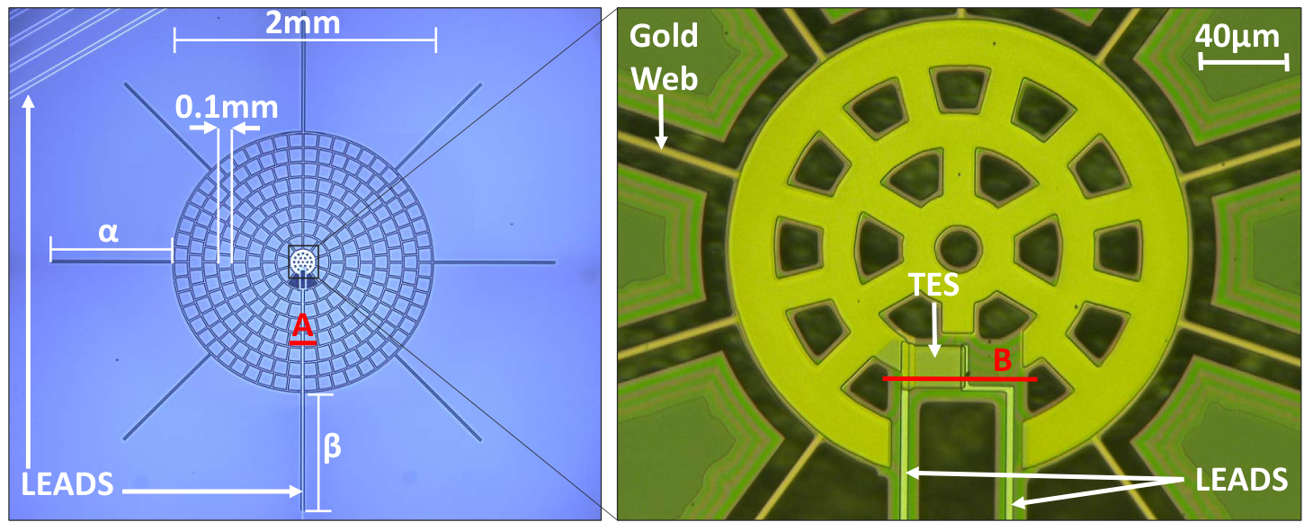
The detectors had spider-web absorber architecture similar to the TESs used for the APEX-SZ and SPT-SZ experiments [42, 12, 60, 71, 72]. The design of a single TES, shown in Figure 9, consisted of a low-stress silicon nitride, gold-metalized web that served as the absorber for millimeter-wave radiation. The web was suspended above the silicon wafer by 8 legs, which provided thermal isolation, and were used to tune the thermal conductance of the bolometers. A TES made of aluminum-titanium superconducting proximity bilayer in the middle of the web was operated at its transition temperature, typically between 0.4 and 0.5 K. Two niobium leads delivered constant voltage bias and monitored current fluctuations.
Table 2 gives the bolometer design parameters for the three EBEX frequency bands, including the TES electrical resistance in the normal state (), TES transition temperature (), average thermal conductance (), bolometer geometry parameters and described in Figure 9, the expected heat capacity () of the bolometers, and the intrinsic optical time constant (). The choice of some of the design parameters, most notably the thermal conductance, reflects the unique demands of a balloon flight; the in-flight optical loading is not a-priori known, and once the instrument is conducting observations there is no opportunity for further detector optimization. Therefore the thermal conductance must have sufficient margin, that is, must be large enough, to ensure the detectors can operate over a relatively broad range of optical loadings. A consequence is that with nominal optical load a larger detector voltage bias is required, which reduces the responsivity and amplifies readout noise equivalent power.
| Band (GHz) | 150 | 250 | 410 | |||
|---|---|---|---|---|---|---|
| Design | Measured | Design | Measured | Design | Measured | |
| () | 1.5 | 1.9 | 1.5 | 1.5 | 1.5 | 1.4 |
| (K) ‡ | 0.44 | 0.45 | 0.44 | 0.48 | 0.44 | 0.47 |
| (pW/K) | 19 | 39 | 45 | 54 | 63 | 63 |
| (ms) | 17 | 88† | 13 | 46† | 10 | 57† |
| (pJ/K)* | 0.5 | 3.8† | 0.9 | 3.3† | 1.0 | 8.4† |
| Wafer thickness (m) | 150 | 90 | 56 | |||
| (mm) | 1.05 | 1.0 | 0.5 | |||
| (mm) | 1.45 | 1.0 | 0.5 | |||
| ‡ Design values calculated early in the program using thermal conductivity power index and | ||||||
| a bath temperature of 260 mK. | ||||||
| † Median of measurements on a single wafer at each frequency; see Section V.2.4. | ||||||
| * Calculated from time constant and thermal conductance. | ||||||
V.1.1 TES, Absorber, and Backshort
The TESs were constructed from a 110 nm titanium layer deposited on top of a 40 nm aluminum layer in a single vacuum step. We chose a transition temperature of 0.44 K to minimize phonon noise given the expected 0.25 K focal plane temperature [65]. The normal resistance for all bands was 1.5 to ensure that the detector operated in the stable regime [21].
A metalized spider-web structure appears as a continuous sheet of metal with resistivity to electromagnetic radiation of wavelength incident upon it as long as the grid spacing satisfies [11]. In addition, the return loss remains below -10 dB when is between 150 and 700 /sq [24]. The EBEX web grid spacing was 100 m, 7 times smaller than the shortest wavelength admitted, and we used 200 thick layer of gold to achieve = /sq.
The absorption efficiency of the detector depends on the distance of the backshort from the absorber. Within a single uniform silicon medium the optimal distance is /4, where is the wavelength in solid silicon behind the web absorber; = , where is the wavelength in empty space and = 3.4 is the index of refraction of silicon [40, 52]. To achieve these backshort thicknesses we etched the detector wafers to thicknesses of 150, 90, and 56 m for the 150, 250, and 410 GHz bands, respectively. However, these wafer thicknesses were too thin to survive standard micro-fabrication techniques and we thus bonded the bolometer wafer to a thicker backing wafer to provide additional mechanical stability [71, 72]; see Figure 10.
When we include in the absorption simulation the 30 m cavity behind the web absorber, which makes the backshort a combination of two media, we find that the expected absorption efficiency is 35% at 410 GHz, and 75% for the other two bands.
V.1.2 Thermal Conductance
Table 2 gives our specifications for the average thermal conductance for each of the frequency bands. We arrived at these specifications by conservatively requiring that the bolometer handle total absorbed powers of up to 4, 9 and 12 pW for each of the 150, 250, and 410 GHz bands, respectively, before the TES exits the superconducting transition. We set these requirements early in the development of instrument by calculating the expected optical loads from both sky and instrument sources and by applying a safety factor to account for unexpected loads. We find that our conservative specifications are met when comparing to the measurement of the in-flight total optical load described in Section V.3.
Of the two contributions to the thermal conductance of the bolometer, (i) the silicon nitride legs that connected the web to the wafer, and (ii) the two niobium electrical leads, the thermal conductance of the niobium leads was negligible [36, 72]. Therefore, we achieved different thermal conductances for each frequency band through changes in the geometry of the silicon nitride legs. The geometry of the legs and the calculated average thermal conductances are given in Figure 9 and in Table 2.
V.1.3 Intrinsic Time Constant
The intrinsic optical time constant of the bolometer is set by the ratio of the heat capacity at the operating temperature to the differential thermal conductance : . The predicted heat capacity of the bolometer was dominated by the contributions of the TES and the gold absorber layer, which gave 80% and 20% of the total, respectively. The calculated contributions of the silicon nitride web and niobium leads were calculated to be negligible [72, 69]. Since the TES and gold layer were identical among the frequency bands, changes in the time constant with frequency band were a result of differences in thermal conductance. Table 2 gives the design values of for each of the frequency bands. The table quotes the average thermal conductance , which is related to the differential value through
| (2) |
where is the bolometer bath temperature and following conventions we assumed power law dependence for the differential thermal conductance . We used = 2 since thermal conductivity measurements of engineering flight wafers gave values of 2.2 0.3, 1.9 0.2, and 2.1 0.2 for the 150, 250, and 410 GHz bands, respectively [30, 4].
V.2 Detector Characterization
We characterized the properties of all 14 detector wafers that were included in the EBEX2013 flight. Characterization included testing for electrical continuity of each detector before a wafer was wire-bonded with an LC board and a standard set of measurements at cryogenic temperatures in dark conditions. In dark conditions, the wafer was mounted inside a sealed box cooled to 0.32 K and thus was subjected to an optical power load of 9 fW, which is two orders of magnitude smaller than expected in-flight conditions.
There were 140 bolometers fabricated on a single EBEX wafer, of which we could read out 124 with the edge, and 127 with the central, LC boards. This gave a total of 1960 bolometers from which 1742 could be read out, as listed in the first two lines of Table 3. We now enumerate further reductions in detector yield. At room temperature, each bolometer was inspected visually under a microscope and also probed across its bond pads for electrical continuity (line 3). To monitor noise, some electronic channels read out resistors located on the LC boards (two per wafer), four combs were attached to dark SQUIDs that did not have bolometers, and one SQUID had an electronic malfunction (line 4). Some bolometers which had electrical continuity at room temperature did not have continuity during the cold (0.8 K) network analysis (line 5). Of the 112 SQUIDs 5 failed to tune (line 6). Those bolometers whose operation drastically worsened the noise performance of their entire comb were disconnected (line 7). The number of bolometers that had successful I-V curves during first tuning at float is given in line 8.
| Frequency (GHz) | |||||
| Count of | 150 | 250 | 410 | Total | |
| 1 | detectors on wafers | 1120 | 560 | 280 | 1960 |
| 2 | maximum detectors to read out | 992 | 496 | 254 | 1742 |
| 3 | detectors which passed warm electrical & visual inspections | 908 | 455 | 232 | 1595 |
| 4 | channels wired to detectors which | ||||
| passed warm electrical & visual inspections | 861 | 447 | 213 | 1521 | |
| 5 | detectors which passed the 0.8 K network analysis test | 805 | 430 | 187 | 1422 |
| 6 | detectors after SQUID failures removed | 773 | 414 | 155 | 1342 |
| 7 | detectors after noise polluters removed | 676 | 371 | 133 | 1180 |
| 8 | detectors with successful flight IV curves | 504 | 342 | 109 | 955 |
V.2.1 Resonant Frequencies
We determined the resonant frequencies for each comb of frequencies by maintaining the detectors at 0.8 K, that is, above their transition temperature, and sweeping the bias frequencies between 0.1 and 1.3 MHz. The RLC circuit resonated at its characteristic frequency such that the entire sweep gave a response as shown in Figure 11. A fit of the peak of the resonance with a model of the circuit that accounts for current leakage to all resonators gave the resonant frequencies and the normal resistances of the TESs in the comb [3]. Missing peaks in this measurement corresponded to opens in electrical lines.


Figure 12 gives histograms of the measured normal resistance values for each frequency band. The 150 and 410 GHz bimodal distributions were due to detector parameters being closely grouped within a single fabrication run, but varying between fabrication runs. The measured value of for the 250 GHz band closely matched the design (see Table 2). For the other two frequency bands, one mode of the distribution closely matched while the other mode was higher (lower) than design for the 150 (410) GHz band. The 150 GHz detectors with a measured of 1.9 , instead of the nominal 1.5 , were calculated to have increased electrical cross-talk from a value of 0.5% to 0.8% and decreased loop-gain by 30%. The 410 GHz detectors with a measured of 1.4 were calculated to have increased Johnson noise by 4% relative to the nominal expected value of 4.0 pA .


V.2.2 Transition Temperature
For the measurement of the critical temperature we biased the detectors with 5 nV such that the Joule heating of 1.5 fW was small and the bath temperature was a good proxy for the bolometer’s temperature. For the same reason, the measurement was done in dark conditions. We slowly changed the detectors’ temperature while monitoring the current through the TES. At the critical temperature the current showed a steep transition. Figure 13 shows histograms summarizing the measured critical temperatures. There was a 20% wafer-to-wafer spread in the measured with the medians for the three bands within 11% of the target value of 0.44 K. The 150 GHz detectors have the widest spread of measured . The effect of this spread is twofold: (1) it increases Johnson (phonon) noise when is above (below) the design value, and (2) it increases (decreases) the detector saturation power when the is above (below) the design value. At the high (low) edge of the distribution with = 0.59 K (0.34 K), there was an 16% (14%) increase (decrease) in the calculated Johnson noise relative to the nominal expected value of 4.0 pA/ and an 80% (68%) increase (decrease) in the calculated phonon noise relative to the nominal expected value of 13 aW/. On the low edge of the distribution, the critical temperature causes the 150 GHz detectors to saturate, leaves the responsivity unchanged for the 250 GHz bolometers, and increases the responsivity by 66% for the 410 GHz bolometers. The responsivity is decreased by 110, 56 and 60% for the 150, 250 and 410 GHz bolometers, respectively, on the high edge of the distribution, increasing the readout and Johnson noise relative to phonon and photon noise.


V.2.3 Average Thermal Conductance
We determine the average thermal conductance of the bolometers using the relation
| (3) |
The ‘saturation power’ is the power necessary to operate the TES in the regime of strong electrothermal feedback in which the total power absorbed is constant. This power depends on the bath temperature
| (4) |
Here is the electrical power absorbed in Joule heating and is the radiative power absorbed. In dark conditions we assume that = 0, and so = is therefore a measurable quantity; we added the subscript d to to highlight that this is the electrical power measured in dark conditions.
Histograms summarizing the measured average thermal conductance values for the three EBEX frequency bands are shown in Figure 14. The values of are given for the EBEX bath temperature = 0.25 K. The measurements were conducted in three different cryostats, each operating at a different bath temperature . We corrected the measured values to using the scaling
| (5) |
which assumes that the differential thermal conductance follows a power law ; see Section V.1.3. The design and median of measured values for the average thermal conductances are given in Table 2. There is appreciable spread in the measured values. This spread is a consequence of variance between wafers and is also apparent in the measurements of . Higher thermal conductance increases phonon noise. For example, for a median 250 GHz detector, phonon noise increased by 10% relative to the nominal value of 20 aW/. Higher thermal conductance also increases the required electrical power, decreasing responsivity, which scales as 1/. With a lower responsivity, noise sources that produce fixed current such as readout noise, are referred to higher noise equivalent power values. In this manner, higher thermal conductance effectively amplifies readout noise.


V.2.4 Detector Time Constants
The effective time constant of the bolometer is given by
| (6) |
where is the loop-gain of the bolometer [43].
During the course of the EBEX project we measured time constants in various configurations including a flashing LED (LED) as part of ‘dark’ measurements, chopping between two optical loads [30, 54], using the phase and amplitude methods during polarization calibration, as described in EP1 and in Klein [37], and assessing the shapes of cosmic-ray events during flight. Here we report the results from measurements conducted post-flight on three wafers. In contrast with previous measurements, the post-flight ones were all done in identical conditions, using the same method, and have good detector statistics. Each of the three wafers had detectors fabricated for a different frequency band. For the 150, 250, and 410 GHz band wafers there were 88, 97, and 88 active bolometers, respectively.


We used a dedicated cryostat to operate one wafer at a time in dark conditions and at a bath temperature of 0.32 K. We measured at various operating points along the superconducting transition as quantified by fractions of bolometer normal resistance . We used LEDs with a center wavelength of 940 nm and intrinsic time constant of 1 s to excite the bolometers. The LED was flashed on/off at 13–16 frequencies from 0.1 to 80 Hz for 2 min at each frequency. We calculated the power spectral density of the time stream, removed the background, fit a Fejer kernel [70] to the peak centered on the flash frequency, and extracted the power under the peak from the fit. We plot the response as a function of flash frequency, fit to a single pole function
| (7) |
where is an arbitrary amplitude at , extract the 3 dB cut-off frequency , and convert it to the bolometer time constant
| (8) |
Figure 15 shows a selection of these measurements that are normalized to unity through division by their normalization values . For each measurement we extracted the error from the fit’s covariance matrix and propagated it to calculate . We kept those measurements of for which and ms. For each wafer the cuts removed between 20% and 50% of the measurements at each point in the transition.
The measured distributions of for the 150 GHz bolometers are shown in Figure 16. For each wafer and transition depth we found the median of the distribution and plot the medians as a function of transition depth. On all three wafers the width of the distribution was dominated by variations between detectors rather than measurement errors; typical values were 1 ms. For all three wafers qualitatively followed the expectation of , since increases deeper in the transition; see Figure 16.

We measured by assuming 1 at the highest bias point, 0.98 , so ; median values are given in Table 2. They are longer than design values by factors of 4–6. We combined the measurements of with independent measurement of to infer bolometer heat capacities. For each bolometer we calculated according to Equation 2 using measured , , , and a 0.32 K bath temperature. We calculated for each bolometer and give the design and median of measured values in Table 2. We find that the median heat capacities are larger than design values by factors of 4–8. There are two possible sources for a larger than expected heat capacities: larger specific heats or larger volumes. We measured the thicknesses of the various layers deposited to make the bolometers and find that the volumes were within 15% of design values.
We provided an approximate value for the time constants in flight by extrapolating the thermal conductance to the in-flight 0.25 K bath temperature, and by accounting for changes in due to the lower electrical bias of the detectors, which was a consequence of higher in-flight optical load. We did not attempt to correct for differences in because the derivatives were noisy. The calculated for the three bias points used in flight are shown in Figure 16. During the majority of flight, bolometers were tuned to 0.85 .
V.3 Radiative Load
Equation 4 quantifies the balance of power between a bolometer and its thermal bath when the total power absorbed is constant. , which depends on the thermal conductance, the transition temperature, and bath temperature, has a characteristic value for each detector and was measured for the majority of the detectors in dark conditions. Although these measurements were done at different bath temperatures , they were corrected to the operating temperature in flight using Equation 5. We use Equation 4 to infer the radiative power absorbed in flight
| (9) |
where the subscripts d and f denote dark and in-flight conditions, respectively. Figure 17 shows an example of a 150 GHz detector for which = 4 pW. The electrical power dissipated is plotted as a function of the voltage across the bolometer in dark and flight conditions; these are commonly called ‘load curves’. The difference of 4 pW is measured at the lowest power points of the two load curves, the points at which the bolometer had just entered the constant power operating regime. To ensure stability we operated the detectors as they just entered this regime, that is, relatively high in the superconducting transition. For the majority of the flight the detectors were operated at 85% of their normal resistance.

Figure 18 shows the distribution of the radiative load measured by all detectors. We used the load curves measured during the first tuning at float altitude. The elevation (zenith) angle of the telescope was 60∘ (30∘). We measure an average load of 3.6, 5.3, and 5.0 pW for the 150, 250, and 410 GHz detectors, respectively.


V.4 Optical Efficiency
The end-to-end instrument efficiency for a given detector, defined as the ratio of radiative power absorbed by the detector to the radiative power incident on the instrument , is the product of the telescope’s transmission and the bolometer absorption efficiency
| (10) |
Here is the radiative power incident on a bolometer.
The transmission of the telescope is the product of the transmissions of each of the optical elements. These transmission coefficients were measured or calculated from first principles [3, 75] and are summarized in Tables 4 and 5 for the flight and ground measurement configurations, respectively. For absorption we used the optical path length of a representative detector in a given frequency band and extrapolated cryogenic loss tangent values to our temperatures [34].
| Element | 150 GHz | 250 GHz | 410 GHz |
|---|---|---|---|
| Primary mirror | 1.00 | 1.00 | 1.00 |
| Secondary mirror | 1.00 | 1.00 | 1.00 |
| Cryostat window | 0.97 | 0.96 | 0.97 |
| Thermal filter type 4 | 0.95 | 0.95 | 0.95 |
| Thermal filter type 4 | 0.95 | 0.95 | 0.95 |
| Thermal filter type 3 | 0.98 | 0.98 | 0.98 |
| Teflon filter | 0.96 | 0.95 | 0.93 |
| Thermal filter type 3 | 0.98 | 0.98 | 0.98 |
| LPE1 filter | 0.98 | 0.94 | 0.98 |
| Thermal filter type 4 | 0.95 | 0.95 | 0.95 |
| LPE2 filter | 0.96 | 0.96 | 0.98 |
| Field lens | 0.97 | 0.97 | 0.95 |
| LPE2b filter | 0.97 | 0.99 | 0.91 |
| HWP | 0.94 | 0.93 | 0.91 |
| LPE2b filter | 0.97 | 0.99 | 0.91 |
| Pupil lens #1 | 0.97 | 0.96 | 0.97 |
| Pupil lens #2 | 0.97 | 0.96 | 0.96 |
| Polarizing grid | 0.50 | 0.50 | 0.50 |
| Camera lens | 0.97 | 0.96 | 0.97 |
| Low-pass-blocker | 0.96 | 1.00 | 0.96 |
| Low-pass-edge | 0.86 | 0.95 | 0.96 |
| Feedhorns | 1.00 | 1.00 | 1.00 |
| Waveguides | 1.00 | 1.00 | 1.00 |
| Total | 0.23 | 0.24 | 0.21 |
| Element | 150 GHz | 250 GHz | 410 GHz |
|---|---|---|---|
| Thermal filter type 1 | 1.00 | 0.97 | 0.93 |
| Thermal filter type 2 | 0.97 | 0.96 | 0.90 |
| Teflon filter | 0.96 | 0.95 | 0.93 |
| Thermal filter type 3 | 0.98 | 0.98 | 0.98 |
| LPE1 filter | 0.98 | 0.94 | 0.98 |
| Thermal filter type 4 | 0.95 | 0.95 | 0.95 |
| LPE2 filter | 0.96 | 0.96 | 0.98 |
| Field lens | 0.96 | 0.97 | 0.95 |
| LPE2b filter | 0.97 | 0.99 | 0.91 |
| HWP† | 0.54 | 0.53 | 0.51 |
| Pupil lens #1 | 0.97 | 0.95 | 0.96 |
| Pupil lens #2 | 0.97 | 0.95 | 0.96 |
| Grid | 0.50 | 0.50 | 0.50 |
| Camera lens | 0.97 | 0.96 | 0.97 |
| Low-pass-blocker | 0.96 | 1.00 | 0.96 |
| Low-pass-edge | 0.86 | 0.95 | 0.96 |
| Feedhorns | 1.00 | 1.00 | 1.00 |
| Waveguides | 1.00 | 1.00 | 1.00 |
| Total | 0.16 | 0.15 | 0.12 |
| † At the time of this test the HWP had no antireflection coating. | |||
The calculation of efficiencies required knowledge of the response of the instrument as a function of frequency. These measurements were reported in EP1. The bolometer efficiencies we report here are average efficiencies
| (11) |
where and define the bandwidth of the instrument . An absorption efficiency per band is given Table 6 and the results are discussed in Section V.4.4.
In this section we give constraints on using three types of measurements: (a) Galactic plane scans; (b) laboratory cold load, and (c) comparison of laboratory and in-flight optical loads. Only the laboratory cold load measurement is purely laboratory-based.
V.4.1 Galactic Plane Scans
We used passes across the Galactic plane to calibrate the end-to-end response for each detector [5]. We assumed the Galactic signal is a sum of Planck component maps, which have been scaled to and integrated over each of the measured bands, see Appendix A for more details. We determined the calibration factor (in units of W/count) that gave the conversion from power incident on the instrument to current flowing through a bolometer in readout system counts. We related the current in each bolometer in counts to the power absorbed using the current responsivity (A/W) and the conversion from current measured in readout system counts to physical units (A/count), which was measured in the lab and assumed to be the same for all detectors
| (12) |
Using Equations 10 and 12, the calibration factor is now
| (13) |
from which we find
| (14) |
For the responsivity we assumed the slow signal limit and that the detector had large loop-gain such that
| (15) |
where was the bolometer’s known voltage bias corrected for the effects of stray impedance [43]. Figure 19 shows the distributions of inferred average bolometer absorption efficiencies using the calibration factors for all sections of flight and for all detectors. (The calibration factors varied between different sections.) In Table 6 we report the median of each distribution as the absorption efficiency for the respective band. Additional discussion is given in Section V.4.4.


| Method | 150 GHz | 250 GHz | 410 GHz |
|---|---|---|---|
| Scans of Galactic plane | 0.9 | 0.4 | 0.3 |
| Cold load | 1.0 | 0.3 | 0.2 |
V.4.2 Laboratory Cold Load
We coupled the receiver to a throughput filling, temperature-adjustable cold load. The cold load was constructed to have an emissivity close to 1 in our frequency bands. We set the temperature of the cold load to several values between 25 and 50 K and at each temperature measured the electrical power necessary to operate the bolometer in transition. Similar to Equation 9, the radiative power absorbed by the bolometer in this configuration is given by
| (16) |
where the subscript cl denotes ‘cold load’. Note that in contrast to Equations 4 and 9 the parametrization of power in Equation 16 is in terms of the load temperature. Following the left side of the equation, we measured the absorbed radiative of each bolometer by differencing the measured saturation power (from the measurement in dark conditions) and the measured electrical power in each of the cold load temperatures. This radiative load is linearly proportional to the radiative load incident on the instrument , which we calculated using the spectrum of a black-body load of known temperature, the instruments’ frequency bands, and the transmission efficiencies given in Table 5. The cold load measurement was done for one wafer in each frequency band.
Figure 20 shows an example of as a function of the cold load temperature for one 150 GHz detector, as well as a best-fit model from which we extract its . The Figure also shows the distribution of derived bolometer absorption efficiencies for each frequency band. The medians of the distributions are reported in Table 6. Additional discussion is given in Section V.4.4.


V.4.3 Comparison of Laboratory and in-Flight Optical Loads
A combination of Equations 9 and 10 gives
| (17) |
where is the radiative power incident on the instrument in flight. We find
| (18) |
where is the radiative power incident on the bolometer in flight.
We calculated the power incident on the detectors by including contributions from the sky (CMB and atmospheric emission [6]), the mirrors, other optical elements along the optical path, such as the vacuum window and absorptive filters, and the transmission coefficients listed in Table 4 [3]; see Table 7. The electrical powers in Equation 18 were known from laboratory and in-flight load curve measurements (see Section V.3). We found median bolometer absorption efficiencies of 3.4, 1.1, and 0.7 for the 150, 250, and 410 GHz bands, respectively. Bolometer absorption efficiencies larger than 1 are unphysical and we discuss this result in the next Section.
| Element | 150 GHz | 250 GHz | 410 GHz |
| (pW) | (pW) | (pW) | |
| CMB | 0.063 | 0.032 | 0.0047 |
| Atmosphere | 0.0054 | 0.064 | 0.37 |
| Mirrors | 0.19 | 0.45 | 0.76 |
| Instrument | 0.36 | 1.3 | 3.5 |
| Total | 0.62 | 1.8 | 4.7 |
V.4.4 Discussion of Absorption Efficiency Results
The calibration and cold load measurements give approximately consistent results; a relatively high absorption efficiency at the 150 GHz band and medium absorption at the 250 and 410 GHz bands. The calibration measurement is based on the response to changes in the signal level as the instrument passes across the Galactic plane. The scatter in the histograms of Figure 19, which gives some values that are larger than 1, is due primarily to larger uncertainty in the Galactic calibration for some of the detectors. The other two measurements are sensitive to the total power absorbed in the detector. The cold load measurement also has some scatter due to noise or systematic errors in the calculation of the absorbed power. For example, it is sometimes challenging to accurately estimate from the load curves such as shown in Figure 17.
The results giving absorption efficiencies larger than 1 for the load curve-based measurement indicate that the denominator in Equation 18 had been underestimated and that there was excess load that was not accounted for by the sources listed in Table 7. To find the magnitude of the excess absorbed load we difference the measured and expected values. The measured loads are 3.6, 5.3, and 5.0 pW for the 150, 250, and 410 GHz bands, respectively; see Section V.3. The expected absorbed load is inferred from the product of the expected load incident on the bolometer, as given in Table 7, and the bolometer absorption efficiencies coming from the Galaxy calibration; see Table 6. We find excess absorbed load of 3.1, 4.6, and 3.6 pW for the 150, 250, and 410 bands, respectively. These excess loads were not observed with the laboratory cold load. We note that the design values for the thermal conductances were based on power saturation values of 4, 9, and 12 pW, respectively; see Section V.1.2. Relative to our pre-instrument construction estimates, we find a reduction in sky signal and increase in instrumentally induced load that give a total load consistent with our margin of safety. The reduction in sky signal was a result of having bands with transmission that was approximately half that expected relative to top-hat bands with the same edges.
We hypothesize that beam spill-over past the vacuum window and onto warm surfaces outside of the receiver – here we view the beam as emanating from the focal plane toward the sky – gave rise to the excess load. This spill-over was not detected with the cold load because the load was mounted onto the vacuum window flange and therefore intercepted the entire throughput.
V.5 Noise Performance
We used flight data to quantify individual-detector and overall instrument noise and compare it to expectations. The NEP , which for brevity we also refer to as ‘noise’, consists of several terms
| (19) | |||||
where is Planck’s constant, is the center of the observation frequency band, is a unitless number between zero and one quantifying the photon correlation, is a unitless number between zero and one accounting for the temperature gradient along the link from the TES to the bath, is Boltzmann’s constant, is the TES temperature, and is the TES resistance [47].
Time ordered data from flight is used to directly assess , that is, the left side of Equation 19. We used several configurations to assess the contributions of specific terms on the right side of Equation 19. For each configuration we compared the measurement to expectations. We then combined the contributions in quadrature and compared to the total measured noise . We determined the combination of and using measurements when the detectors were biased above their superconducting transition, using the measured thermal conductances and critical temperatures, and using the measured radiative load.
To assess any noise contribution using flight data, we divided the data into segments of 172 s length and made use of all possible segments. Momentary glitches such as cosmic ray hits were replaced with white noise realizations. Sections of data that had more than 10% of their samples flagged as glitches were excluded from the analysis. For each section we removed an offset and a gradient, applied a Hann window, and calculated the spectral density. For the assessment of the readout and Johnson noise, the data was converted from raw digital units (counts) to current referred to the SQUID input (A) using Equation 1. For the assessment of the total NEP, these data were converted from current through the SQUID to power absorbed at the detector by applying the current responsivity
| (20) |
For each section of data we find the mean level of the spectral density between 3.9 and 4.4 Hz, which is one of the polarization frequency sidebands.


V.5.1 Johnson and Readout Noise
When the detectors were biased above their superconducting transition – we will use the shorthand ‘overbiased’ – the current responsivity was low and the last two terms in Equation 19 should dominate the overall noise. The spectral density for one section of such data for one detector is shown in the left panel of Figure 21. The measurement is shown in units of A/ following Equation 1 since both and are intrinsically current noise sources. To assess noise level over time we calculated such spectral density for all valid sections over 1.7 hours of data, about 35 sections per detector. We find that within 20% the noise levels recorded are stable; see the right panel of Figure 21. Higher variations are expected as compared to the resistor case in Section IV.3 since overbiased detectors have residual sensitivity to stage temperature variations and incident power.

| Wafer | Expectation | Measured/expected ratio |
| (pA/) | ||
| 150-09 | 20 | 1.1 |
| 150-14 | 18 | 1.3 |
| 150-15 | 18 | 0.9 |
| 150-39 | 22 | 0.8 |
| 150-43 | 24 | 1.0 |
| 150-47 | 24 | 1.0 |
| 250-23 | 22 | 1.0 |
| 250-24 | 26 | 0.9 |
| 250-29 | 21 | 1.2 |
| 410-28 | 32 | 1.0 |
| All detectors | 1.0 |
For each detector we calculated the predicted readout noise using the electronic specifications of each element of the readout chain [3]. To estimate the Johnson noise we assumed a detector resistance as inferred from the network analysis, and a detector temperature , where is the difference between the electrical power dissipated when the detector is overbiased and measured in dark conditions. We added the predicted contributions from readout and Johnson in quadrature to find a combined noise term (in A/). We multiplied this term by a factor 1.7. This is the factor which accounts for the excess noise that was observed with the resistor measurements described in Section IV.3.1. The expected levels shown in Figures 21 and 22 include this extra factor. For each detector and for all sections over the given 1.7 hours of data we formed the ratio of measured to expected noise and found the median. A histogram of the medians for all detectors is shown in Figure 22. Table 8 gives the median ratios for each wafer. The median ratio for all detectors is 1.0.
There was excess noise identified with resistor channels in SectionIV.3 amounting to a factor of 1.7 higher than predictions. When this excess is added to predictions of bolometer noise in the overbias state we find consistency with measurements. We noted in Section IV.3.1 that noise measurements in the overbias state after the North American engineering flight did not exhibit this excess noise. The ratio of measured to predicted noise was 1.0 [4]. These measurements were done in the flight receiver, but the receiver was in the laboratory, without other electromagnetic interference (EMI) sources such as attitude control motors and telemetry transmitters. We therefore hypothesize that EMI contributed additional noise that is most apparent in configurations in which the Johnson and readout noise terms dominate.
V.5.2 Noise Equivalent Power in Transition
The total noise when the detector operates in its superconducting transition is given by Equation 19. We report on measured using flight data after removal of the HWPSS (see Section III). We used all the data that passed quality cuts to be used for astrophysical analysis but also included additional data that would otherwise not be used because of, for example, large pointing errors or scan speeds that were too low.


The NEP as a function of time throughout flight for one 150 GHz detector is shown in Figure 23 along with the expected value. We describe the calculation of the expected value in the next paragraph. As before, we found a representative value for the ratio of measured-to-expected NEP throughout flight for a given detector by finding the median over all sections. We combined the medians for each detector to find a median per wafer, which is reported in Table 9. A median measured NEP per frequency band is given in Table 10. Figure 23 gives a histogram for the medians of measured-to-expected ratio for all detectors.
| Wafer | Expected NEP [aW/] | Measured/expected ratio |
|---|---|---|
| 150-09 | 69 | 1.1 |
| 150-14 | 48 | 0.7 |
| 150-15 | 57 | 1.1 |
| 150-39 | 77 | 1.1 |
| 150-43 | 56 | 1.2 |
| 150-47 | 64 | 1.3 |
| 250-23 | 92 | 1.1 |
| 250-24 | 78 | 1.4 |
| 250-29 | 98 | 1.4 |
| 410-28 | 103 | 1.6 |
| All detectors | 1.2 |
We calculated an expected NEP by finding the theoretical Johnson and readout current noise terms and multiplying them by (1) a factor of 1.7 coming from the excess noise in the resistor measurements (see Section IV.3.1), and (2) by an additional factor per wafer as listed in Table 8. The second factor has been identified through the noise measurement with overbiased detectors (see Section V.5.1). To convert from current noise to NEP we divided the Johnson and readout noise terms by the current responsivity and assumed the high loop-gain limit. We assumed to predict the phonon noise [47]. We calculated photon noise using the measured radiative load per detector, as described in Section V.3. We quote the predicted level for a photon correlation factor of 1. The median predictions decreases by 20% (7%) when using a correlation factor of 0 for the 150 and 250 (410) GHz bands.
For the 150 band the measured noise is broadly consistent with calculations after accounting for the excess noise identified through measurements with resistors. No further excess noise is identified when operating the bolometers in transition. The average noise increase for the 3 (1) wafers at 250 (410) GHz is about 30 (60)% after accounting for the excess noise. This level is at the border or beyond the 20-30% uncertainties in our estimates. This additional source of noise is being investigated, although the small number of available wafers may give a biased impression of trends.
| Noise source | Value () | ||
|---|---|---|---|
| 150 GHz | 250 GHz | 410 GHz | |
| Readout | |||
| Johnson | |||
| Phonon | 22 | 25 | 32 |
| Photon | 32 | 49 | 63 |
| Excess | 43 | 64 | 133 |
| Total | 62 | 88 | 160 |
VI Noise Equivalent Temperature and Map Depth
We estimated the NET in two ways: (1) using the TOD in counts and the calibration factors that convert count to temperature; (2) converting the measured NEP to NET. The term ‘temperature’ refers to equivalent sky CMB temperature fluctuations. In this section we describe the two methods and show that they give consistent results. We then use the measured NET and the instantaneous attitude information to produce depth maps for each of the frequency bands.
VI.1 NET using the TOD and Calibration
For each detector we calculated power spectral densities of 5.7 min sections of calibrated, deglitched, HWPSS-subtracted TOD, and fit them with a three-parameter noise model consisting of red and white noise terms as a function of frequency
| (21) |
The parameters are , the white noise level (in K2/Hz); , the frequency cutoff of the red noise power law (also referred to as , in Hz); and , the red noise spectral index. We used all calibrated data throughout flight that passed quality cuts for astrophysical analysis, see Didier [17], and added other data with valid noise information but that would not pass cuts for making maps. Such data included sections during times at which the attitude reconstruction was poor or the scan speeds were below or above specific thresholds. A polynomial with up to cubic terms in time was subtracted from the TOD before applying a Hann window and calculating the PSD (PSD). Figure 24 shows an example of a PSD and its model fit for one section of the data of a 250 GHz detector.
The fitting – conducted on at least 10 sections of data for each detector, but typically over many hours of data – generated a set of parameters , , and , with which we characterized the noise performance. For each detector we find the three median parameter values over all flight. We histogram these median values for all available detectors per frequency band in Figures 25, 26, and 27. The Figures also give the medians of the distributions.
The data show knee frequencies near 200 mHz and red noise power law index near 2.3. These relatively high values are not intrinsic to the detectors or readout, but rather are a consequence of the azimuth motor malfunction, described in EP3. In the absence of controlled azimuth pointing the payload executed full rotations causing strong Sun-synchronous drifts in the TOD. Removal of a cubic order polynomial from the TOD removes some of the drifts, but remnants are manifest in the statistics of and . A correlation analysis between the noise properties of different detectors showed strong coherency at low frequencies supporting the model of drifts due to Sun-synchronous signals.
VI.2 NET using the NEP
VI.3 Discussion of NET
The two approaches for finding the NET are not independent. Finding NET using the measured calibration factors makes no assumption about the instrument’s transmission efficiency and specific detector absorption efficiency. Finding NET using the NEP does not explicitly depend on the measured calibration factors. However, the conversion from absorbed power to temperature on the sky, as given in Equation 22, depends on the transmission and absorption efficiencies, which were derived – at least in one way of finding efficiencies – using the calibration factors. Therefore the comparison we are providing is a check on end-to-end consistency, rather than a comparison of results using two entirely independent methods.
The measured NETs are consistent within 10% for the 150 and 250 GHz bands. There is a larger difference for the 410 GHz. The estimate from the NEP depends on the product of the instrument’s throughput and efficiency through the multiplicative factor ; see Equation 22. For the throughput we assumed a single mode () for the propagating electromagnetic wave. We hypothesize that at the highest frequency band we are underestimating the throughput by assuming a complete cut-off of the 2nd mode. A 25% higher throughput brings the NET from NEP and NET from calibration to values that agree within our overall uncertainty.
| 150 GHz | 250 GHz | 410 GHz | |
|---|---|---|---|
| NEP (aW/) | 62 | 88 | 160 |
| NET from NEP (K | 380 | 1000 | 23000 |
| NET from Calibration (K | 400 | 920 | 14500 |
VI.4 Map Depth
The high fidelity attitude reconstruction from the EBEX2013 flight was discussed in EP3. We binned all the data that passed quality cuts for making maps using HEALPix [25] with . With each sample we associated an equivalent temperature noise (in K) equal to the product of the NET calculated during that time section and the square root of the sampling rate. We calculated depth per pixel following
| (23) |
where the sum is over all samples that had pointing associated with a given pixel .
The depth maps with pixels of 1 deg2 for the three frequency bands are shown in Figure 28. The noise distribution is strongly inhomogeneous, a consequence of an azimuth motor malfunction, as described in EP3. The median depth values per pixel for the 150 and 250 GHz bands – 11 and 28 K, respectively – are several factors larger than those reported by Planck and the expected CMB E-mode signal. A signal-to-noise ratio above 1 is only achieved for a fraction of the pixels on the Galaxy at 410 GHz. The depth maps do not encode noise and filtering that further degrades the signal-to-noise ratio. We therefore decided not to publish maps.


VII Summary
EBEX was a CMB polarimeter that had two focal planes consisting of 14 detector wafers. Each focal plane had 4 wafers operating at 150 GHz, two at 250 GHz, and a central wafer at 410 GHz. We have presented the design of bolometers optimized for the low optical load in the stratosphere and for operation at 410 GHz, a frequency that is unique for balloon payloads. To handle the thin wafers suitable for this frequency band we have developed a technique to bond them to thicker wafers. We have shown distributions of measured thermal conductances, normal resistances, transition temperatures, and time constants. For the 250 and 410 GHz bands the median thermal conductances were within 20% of design values. For the 150 GHz band, for which our target was 2.4 times lower than for the 250 GHz band, the median measured value was 2 times higher than design. This result reflects the additional challenge in making very low thermal conductance spider-web bolometers operating at 0.25 K. The lower thermal conductance is a consequence of the lower optical load expected at 150 GHz; see Table 7. The measured transition temperatures were within 10% of design values and median measured (design) saturation powers were 7.8 (4), 12 (9) and 14 (12) pW, for the 150, 250, and 410 GHz, respectively. The measured time constants were 3.5 to 5.7 times longer than design values. Either published values for specific heats of the materials that made up the bolometer are incorrect, or the devices had been contaminated by unknown materials during fabrication.
We have measured in-flight median optical loads of 3.6, 5.3, and 5.0 pW, at the three bands, respectively. Given the final configuration of all optical elements inside the instrument and the measured frequency bands, we have calculated the expected contributions from the sky, warm telescope, and instrument emission. The warm mirrors, a teflon filter, and the HWP dominated the expected load. We have also identified excess optical load in flight, but no excess load was measured when we coupled a 4 K load onto the vacuum window of the receiver in the laboratory. We therefore attribute the additional load to spillover of throughput onto warm surfaces outside of the receiver.
Two measurement methods for finding the bolometer absorption efficiencies gave consistent results within 10% for all frequency bands. They indicate high absorption efficiency ( 0.9) for the 150 GHz and medium (medians of 0.35 and 0.25) for the 250 and 410 GHz bands. The measured distributions are broad occasionally giving apparently unphysical absorption values larger than 1. However, noisy measurements that give wide distributions can give values larger than 1.
EBEX was the first experiment to implement the digital version of a frequency domain multiplexing system aboard a balloon payload. For several years it had the highest multiplexing factor of 16 until SPT3G began implementing a multiplexing factor of 64 in 2016. We have developed novel, superconducting, low inductance microstrips. We have measured gain stability of better than 0.25% over 13 hours, and better than 2% over the duration of the flight, even as the temperature of the readout boards experienced temperature excursions of up to 20∘C.
The rotation of the HWP introduced a HWP synchronous signal in the TOD. To assess the noise performance we have fit and removed the synchronous signal. We have given a detailed accounting of the measured noise. The readout noise was measured to match predictions in the laboratory and for dark SQUIDs in flight. We have found excess noise in-flight when analyzing resistor data and when the detectors were in an over-biased state, for which the readout and Johnson noise are expected to be dominant. The median excess noise was a factor 1.7 larger than the expected total of Johnson and readout noise terms. When we included an extra noise term to account for the excess noise observed in the over-bias state the median measured noise in-transition was 20% higher than expectation. We suspect that electromagnetic pickup from telemetry electronics coupling to the long microstrips was the cause for the excess noise.
We have calculated the median NET in two ways and found consistency for the 150, and 250 GHz bands. The pre-flight expectation for 150 GHz, taking into account the high thermal conductivity detectors, but without excess noise or load, was 210 K. For the target thermal conductivity of 19 pW/K, the expectation was 180 K, a factor of 2.2 lower that the achieved value of 400 K. Our expectation of 180 K was higher by a factor of 1.3 compared to the best reported by BOOMERANG [16] (which also had bolometers operated at a bath temperature near 0.25 K) because EBEX had two warm mirrors, not one, higher internal emission from a teflon filter due to a much larger vacuum window, higher temperature for its rotating HWP, and higher detector thermal conductivity than required at 150 GHz. We chose high detector thermal conductance because it mitigated the risk of un-anticipated optical load at the expense of higher noise. This choice proved prudent; we did experience excess load but continued to operate the majority of the bolometers. A next generation balloon-borne instrument that has only one ambient temperature mirror, detectors with appropriately low thermal conductivity, and that applies the lessons learned from EBEX2013 (including having lower internal emission from filters and HWP, and mitigating excess load and noise) can achieve 140 K at 150 GHz.
EBEX was the first balloon experiment to implement a kilo-pixel array of bolometers in the focal plane. It was among the first to face the challenges imposed by a significantly larger focal plane, optical elements, and vacuum window. The EBEX experience suggests the following path for a future experiment with kilo-pixel TES arrays to make optimal use of the balloon environment: (1) reduce instrument emissions through the development and implementation of high thermal conductance, low mm-wave emissivity and reflectivity IR filters and lenses, and by maintaining optical elements at cold temperatures if practical. However, for an experiment that targets a resolution finer than 25 arcmin at 150 GHz, at least one reflector will almost certainly still need to be maintained at ambient temperatures; (2) implement optical elements that are appreciably larger than the nominal optical bundle to mitigate diffraction near apertures and thus reduce spill-over outside the designated throughput, even at the expense of a larger cryostat, larger window, and potentially heavier payload; (3) pay attention to EMI mitigation, as wiring that couples the SQUIDs to the detector focal plane are susceptible to the transmitter-heavy environment on-board the payload. (Since the EBEX2013 flight there have been additional reports of excess noise due to telemetry electronics in other millimeter and sub-millimeter experiments [22, 23].) The EMI integrity of the wiring cavity of the cryostat should be excellent or experiments should impose radio-silence after initial check-up and calibration. Significant time should be allocated to testing in full flight configuration, including telemetry electronics.
Because of the malfunction of the azimuth motor, a result of thermal design error that is discussed in EP3, the instrument scanned 6000 deg2, giving shallow depth with highly inhomogeneous noise. We have presented depth maps that gave a median noise of 11 and 28 K per HEALPix pixel at 150 and 250 GHz. The map noise is higher compared to Planck’s noise as well as to that of other contemporaneous experiments and we did not find it compelling to publish our own maps or power spectra.
EBEX pioneered the use of TES bolometers on a balloon-borne platform. It was the first experiment to fly a small array of these detectors in a test-flight in 2009 and a kilo-pixel array during its EBEX2013 flight. Nearly 1000 bolometers were operating shortly after the payload reached float altitude. EBEX pioneered the use of the digital frequency domain multiplexing readout system. This system is now implemented on several operating ground-based instruments [8, 63, 33] and is baselined for a proposed space mission [64]. EBEX was also the first astrophysics experiment to implement a superconducting magnetic bearing. This system too is baselined for a ground-based and a proposed space mission [28, 32]. EBEX was a successful technology pathfinder for future CMB space missions.
- ACS
- attitude control system
- ADC
- analog-to-digital converters
- ADS
- attitude determination software
- AHWP
- achromatic half-wave plate
- AMC
- Advanced Motion Controls
- ARC
- anti-reflection coating
- ASD
- amplitude spectral density
- ATA
- advanced technology attachment
- BRC
- bolometer readout crates
- BLAST
- Balloon-borne Large-Aperture Submillimeter Telescope
- CANbus
- controller area network bus
- CMB
- cosmic microwave background
- CMM
- coordinate measurement machine
- CSBF
- Columbia Scientific Balloon Facility
- CCD
- charge coupled device
- DAC
- digital-to-analog converters
- DASI
- Degree Angular Scale Interferometer
- dGPS
- differential global positioning system
- DfMUX
- digital frequency domain multiplexer
- DLFOV
- diffraction limited field of view
- DSP
- digital signal processing
- EBEX
- E and B Experiment
- EBEX2013
- EBEX2013
- ELIS
- EBEX low inductance striplines
- EP1
- EBEX Paper 1
- EP2
- EBEX Paper 2
- EP3
- EBEX Paper 3
- EP4
- EBEX Paper 4
- ETC
- EBEX test cryostat
- FDM
- frequency domain multiplexing
- FPGA
- field programmable gate array
- FCP
- flight control program
- FOV
- field of view
- FWHM
- full width half maximum
- GPS
- global positioning system
- HPE
- high-pass edge
- HWP
- half-wave plate
- HWPSS
- half-wave plate synchronous signal
- IA
- integrated attitude
- IP
- instrumental polarization
- JSON
- JavaScript Object Notation
- LDB
- long duration balloon
- LED
- light emitting diode
- LCS
- liquid cooling system
- LC
- inductor and capacitor
- LPE
- low-pass edge
- MLR
- multilayer reflective
- MAXIMA
- Millimeter Anisotropy eXperiment IMaging Array
- NASA
- National Aeronautics and Space Administration
- NDF
- neutral density filter
- NEP
- noise equivalent power
- NET
- noise equivalent temperature
- PCB
- printed circuit board
- PE
- polyethylene
- PME
- polarization modulation efficiency
- PSD
- power spectral density
- PSF
- point spread function
- PTFE
- polytetrafluoroethylene
- PV
- pressure vessel
- PWM
- pulse width modulation
- RMS
- root mean square
- RSS
- rotation synchronous signal
- SLR
- single layer reflective
- SMB
- superconducting magnetic bearing
- SQUID
- superconducting quantum interference device
- SQL
- structured query language
- STARS
- star tracking attitude reconstruction software
- TCP/IP
- Transmission Control Protocol/Internet Protocol
- TDRSS
- tracking and data relay satellites
- TES
- transition edge sensor
- TM
- transformation matrix
- TOD
- time ordered data
- VME
- Versa Module European
Appendix A Calibration
The calibration produces two equivalent conversions, one from measured counts to signal power incident on the instrument, and the other from measured counts to CMB temperature fluctuation of magnitude . In Section V.4.1 we use , which is the conversion from counts to power; (W/count). For completeness, for the purpose of this appendix, we denote as the quantity (K/count), where refers to CMB temperature fluctuation of magnitude (K). To find these calibration factors using passes across the Galactic plane we build reference signal maps at our frequency bands from the Planck component maps described in Planck Collaboration et al. [53]. We use the R2 Planck component maps processed with the Commander framework from https://pla.esac.esa.int/#maps. The reference signal maps are a combination of thermal dust, free-free, CO, and the CMB. Within the EBEX bands and near the Galactic plane the maps are entirely dominated by the dust component.
We now describe the making of the dust intensity map as a function of frequency. Other signal maps, corresponding to other components, are made in the same way using the extrapolation factors provided in Planck Collaboration et al. [53]. The thermal dust amplitude map referred to a baseline frequency GHz is first converted from its native units to intensity (W/sr m2 Hz). The resulting map is then extrapolated to frequency using the frequency scaling factor
| (A1) |
and using the Planck-provided maps of dust temperature and spectral index .
The total incident signal map (at each frequency) is a sum of the individual component signal maps. To find the total incident signal power we integrate the total incident reference signal map over the EBEX bands (as measured and reported in EP1) and multiply by the throughput of the instrument. A linear regression of the power in the reference map vs counts measured by a given bolometer when passing the galactic plane gives for that bolometer.
The total incident signal map (at each frequency) is alternatively converted to using the spectral radiance of a blackbody . It is then integrated as a function of frequency and weighted by the normalized transmission of the instrument. A linear regression of the temperatures in the reference map to the counts measured by a given bolometer when passing the galactic plan give for that bolometer.
References
- [1] Ade, P., Akiba, Y., Anthony, A., et al. 2014, ApJ, 794, doi:2/171
- [2] Araujo, D. 2017, PhD thesis, Columbia University
- [3] Aubin, F. 2012, PhD thesis, McGill University
- [4] Aubin, F., Aboobaker, A. M., Ade, P., et al. 2010, in Proc. SPIE, Vol. 7741, Millimeter, Submillimeter, and Far-Infrared Detectors and Instrumentation for Astronomy V, 77411T–77411T–10
- [5] Aubin, F., Aboobaker, A. M., Bao, C., et al. 2017, The Fourteenth Marcel Grossmann Meeting, 2084
- [6] Bao, C. 2015, PhD thesis, University of Minnesota
- [7] Baumann, D., Jackson, M. G., Adshead, P., et al. 2009, AIPC, 1141, 10
- [8] Benson, B. A., Ade, P. A. R., Ahmed, Z., et al. 2014, Proc.SPIE, 9153, 9153
- [9] BICEP2 Collaboration, Ade, P. A. R., Aikin, R. W., et al. 2014, Physical Review Letters, 112, 241101
- [10] BICEP2/Keck and Planck Collaborations, Ade, P. A. R., Aghanim, N., et al. 2015, Phys. Rev. Lett., 114, 101301
- [11] Bock, J. J., Chen, D., Mauskopf, P. D., & Lange, A. E. 1995, Space Sci. Rev., 74, 229
- [12] Chang, C. L., Ade, P. A. R., Aird, K. A., et al. 2009, AIP Conference Proceedings, 1185, 475
- [13] Chapman, D. 2015, PhD thesis, Columbia University
- [14] Chapman, D., Didier, J., Hanany, S., et al. 2014, in Proc. SPIE, Vol. 9152, Software and Cyberinfrastructure for Astronomy III, 915212
- [15] Chapman, D., Aboobaker, A. M., Araujo, D., et al. 2015, in 2015 IEEE Aerospace Conference, 1–11
- [16] Crill, B. P., Ade, P. A. R., Artusa, D. R., et al. 2003, The Astrophysical Journal Supplement Series, 148, 527
- [17] Didier, J. 2016, PhD thesis, Columbia University
- [18] Didier, J., Chapman, D., Aboobaker, A., et al. 2015, Proc. of IEEE Aerospace Conference
- [19] Didier, J., Miller, A. D., Araujo, D., et al. 2017, in prep
- [20] Dobbs, M., Bissonnette, E., & Spieler, H. 2008, IEEE Transactions on Nuclear Science, 55, 21
- [21] Dobbs, M. A., Lueker, M., Aird, K. A., et al. 2012, Review of Scientific Instruments, 83, 073113
- [22] Galitzki, N., Ade, P. A. R., Angilè, F. E., et al. 2014, in Ground-based and Airborne Telescopes V, Vol. 9145, 91450R
- [23] Gambrel, A. E. 2018, PhD thesis, Princeton University, Princeton
- [24] Glenn, J., Chattopadhy, G., Edgington, S., et al. 2002, Applied Optics, 41, 136
- [25] Górski, K. M., Hivon, E., Banday, A. J., et al. 2005, ApJ, 622, 759
- [26] Grainger, W., Aboobaker, A. M., Ade, P., et al. 2008, in Proc. SPIE, Vol. 7020, Millimeter and Submillimeter Detectors and Instrumentation for Astronomy IV, 70202N
- [27] Hanson, D., Hoover, S., Crites, A., et al. 2013, PhRvL, 111, 141301
- [28] Hill, C. A., Kusaka, A., Barton, P., et al. 2018, Journal of Low Temperature Physics, doi:10.1007/s10909-018-1980-6
- [29] Huber, M. E., Neil, P. A., Benson, R. G., et al. 2001, IEEE Transactions on Applied Superconductivity, 11, 4048
- [30] Hubmayr, J. 2009, PhD thesis, University of Minnesota
- [31] Hubmayr, J., Aubin, F., Bissonnette, E., et al. 2008, in Proc. SPIE, Vol. 7020, Millimeter and Submillimeter Detectors and Instrumentation for Astronomy IV, 70200J–70200J–8
- [32] Iida, T., Sakurai, Y., Matsumura, T., et al. 2017, IOP Conference Series: Materials Science and Engineering, 278, 012011
- [33] Inoue, Y., Ade, P., Akiba, Y., et al. 2016, Proc.SPIE, 9914, 9914
- [34] Jacob, M. V., Mazierska, J., Leong, K., & Krupka, J. 2002, IEEE Transactions on Microwave Theory Techniques, 50, 474
- [35] Johnson, B. R., Collins, J., Abroe, M. E., et al. 2007, ApJ, 665, 42
- [36] Kes, P. H., Rolfes, J. G. A., & de Klerk, D. 1974, Journal of Low Temperature Physics, 17, 341
- [37] Klein, J. 2014, PhD thesis, University of Minnesota
- [38] Klein, J., Aboobaker, A., Ade, P., et al. 2011, in Proc. SPIE, Vol. 8150, Cryogenic Optical Systems and Instruments XIII, 815004–815004–10
- [39] Kovac, J. M., Leitch, E. M., Pryke, C., et al. 2002, Nature, 420, 772
- [40] Lamb, J. W. 1996, International Journal of Infrared and Millimeter Waves, 17, 1997
- [41] Lanting, T. M. 2006, PhD thesis, University of California, Berkeley
- [42] Lee, A. T., Richards, P. L., Nam, S. W., Cabrera, B., & Irwin, K. D. 1996, Applied Physics Letters, 69, 1801
- [43] Lee, S.-F., Gildemeister, J. M., Holmes, W., Lee, A. T., & Richards, P. L. 1998, Applied Optics, 37, 3391
- [44] MacDermid, K. 2014, PhD thesis, McGill University
- [45] MacDermid, K., Hyland, P., Aubin, F., et al. 2009, in American Institute of Physics Conference Series, Vol. 1185, American Institute of Physics Conference Series, ed. B. Young, B. Cabrera, & A. Miller, 253–256
- [46] MacDermid, K., Aboobaker, A. M., Ade, P., et al. 2014, in Proc. SPIE, Vol. 9153, Millimeter, Submillimeter, and Far-Infrared Detectors and Instrumentation for Astronomy VII, 915311
- [47] Mather, J. C. 1982, Appl Opt, 21, 1125
- [48] Milligan, M., Ade, P., Aubin, F., et al. 2010, in Proc. SPIE, Vol. 7740, Software and Cyberinfrastructure for Astronomy, 774007
- [49] Naess, S., Hasselfield, M., McMahon, J., et al. 2014, JCAP, 2014, 007
- [50] NIST. 2010, Private Communication, ,
- [51] Oxley, P., Ade, P. A., Baccigalupi, C., et al. 2004, in Proc. SPIE, Vol. 5543, Infrared Spaceborne Remote Sensing XII, 320–331
- [52] Phillips, T. G., & Zmuidzinas, J., eds. 2003, Proc. SPIE, Vol. 4855, Design and performance of feedhorn-coupled bolometer arrays for SPIRE, ed. T. G. Phillips & J. Zmuidzinas, 510–519
- [53] Planck Collaboration, Adam, R., Ade, P. A. R., et al. 2016, A&A, 594, A10
- [54] Polsgrove, D. E. 2009, PhD thesis, University of Minnesota
- [55] Priestly, M. 1981, Spectral Analysis and Time Series (Academic Press)
- [56] Reichborn-Kjennerud, B. 2010, PhD thesis, Columbia University
- [57] Reichborn-Kjennerud, B., Aboobaker, A. M., Ade, P., et al. 2010, in Proc. SPIE, Vol. 7741, Millimeter, Submillimeter, and Far-Infrared Detectors and Instrumentation for Astronomy V, 77411C
- [58] Sagiv, I., Aboobaker, A. M., Bao, C., et al. 2012, in Twelfth Marcel Grossmann Meeting on General Relativity, ed. A. H. Chamseddine, 2166–2176
- [59] Sagiv, I. S. 2011, PhD thesis, University of Minnesota
- [60] Schwan, D., Ade, P. A. R., Basu, K., et al. 2011, Review of Scientific Instruments, 82, doi:http://dx.doi.org/10.1063/1.3637460
- [61] Scott, D., & Smoot, G. F. 2010, in The Review of Particle Physics, ed. K. Nakamura et al. (J. Phys.)
- [62] Silva-Feaver, M., Arnold, K., Barron, D., et al. 2017
- [63] Stebor, N., Ade, P., Akiba, Y., et al. 2016, The Simons Array CMB polarization experiment, , , doi:10.1117/12.2233103
- [64] Suzuki, A., Ade, P. A. R., Akiba, Y., et al. 2018, Journal of Low Temperature Physics, 124
- [65] Suzuki, A. G. 2013, PhD thesis, University of California, Berkeley
- [66] Takakura, S., Aguilar, M., Akiba, Y., et al. 2017, arXiv:1702.07111
- [67] The EBEX Collaboration. 2016a, ApJ
- [68] —. 2016b, ApJ
- [69] Van Sciver, S. 2012, Helium Cryogenics (Springer), doi:10.1007/BF00751274
- [70] Weiße, A., Wellein, G., Alvermann, A., & Fehske, H. 2006, Reviews of Modern Physics, 78, 275
- [71] Westbrook, B., Lee, A., Meng, X., et al. 2012, Journal of Low Temperature Physics, 167, 885
- [72] Westbrook, B. G. 2014, PhD thesis, University of California, Berkeley
- [73] Yoon, J., Clarke, J., Gildemeister, J. M., et al. 2001, Applied Physics Letters, 78, 371
- [74] Zaldarriaga, M., & Seljak, U. 1997, Phys. Rev. D, 55, 1830
- [75] Zilic, K. 2014, PhD thesis, University of Minnesota