Microwave device characterization using a widefield diamond microscope
Abstract
Devices relying on microwave circuitry form a cornerstone of many classical and emerging quantum technologies. A capability to provide in-situ, noninvasive and direct imaging of the microwave fields above such devices would be a powerful tool for their function and failure analysis. In this work, we build on recent achievements in magnetometry using ensembles of nitrogen vacancy centers in diamond, to present a widefield microwave microscope with few-micron resolution over a millimeter-scale field of view, microwave amplitude sensitivity, a dynamic range of 48 dB, and sub-ms temporal resolution. We use our microscope to image the microwave field a few microns above a range of microwave circuitry components, and to characterize a novel atom chip design. Our results open the way to high-throughput characterization and debugging of complex, multi-component microwave devices, including real-time exploration of device operation.
Microwave (MW) devices play a critical role in telecommunications, defence, and quantum technologies. Device characterization via high resolution MW field imaging is a long-standing goal [1, 2, 3], which promises to overcome the limitations of conventional characterization techniques. For example, it is difficult to identify internal features of complex devices using S-parameter measurements of reflection and transmission through external device ports [4, 5]. A high-throughput MW imaging method would allow for fast prototype iteration, and for more adventurous development of novel device architectures. Furthermore, MW imaging is of interest for spin-wave imaging in magnonic systems [6, 7], is under investigation for medical imaging [8, 9], and can be used to characterize materials [10] and biological samples [11]. In recent years, alkali vapor cells with atoms in the ground [12, 13, 14, 15, 16] or highly excited Rydberg [17, 18, 19] states, and nitrogen-vacancy (NV) centers in diamond [20, 21, 22, 23] have shown promise for intrinsically calibrated MW imaging in simple, vacuum- and cryogen-free environments. Ensembles of NVs in a widefield diamond microscope [24, 25, 26, 27, 28] provide an excellent balance between the sensitivity and wide field of view (FOV) offered by vapor cells and the nanoscale spatial resolution of single NV centers [29], and so far have been primarily employed for imaging static and low-frequency magnetic fields. In this work, we demonstrate high-throughput widefield diamond microscopy for MW device characterization, enabled by a step-change we have achieved in microscope performance.
Our microscope integrates advances in camera speed, experiment control, novel diamond material, laser illumination, and the use of an intrinsically calibrated MW sensing scheme, to perform MW imaging with an unprecedented combination of temporal resolution, FOV and spatial resolution. We demonstrate a 0.5 mm2 FOV with few-micron spatial resolution, a MW amplitude sensitivity of , and a dynamic range of 48 dB. We have advanced the temporal resolution to the sub-ms regime, an order of magnitude beyond the previous state of the art [22], enabling dynamic probing of circuit operation, and real-time exploration of large-scale devices by scanning them under the microscope (Supplementary Movies 1, 2 [30]). In addition, the accessible design of our microscope enables high-throughput measurements with rapid exchange of MW devices, demonstrating its applicability to industry-relevant environments.

I Microwave Imaging with the Widefield Diamond Microscope
Our imaging goal is to determine the spatial profile of an inhomogeneous MW field of known frequency. We perform measurements by driving oscillations on an NV MW transition and measuring the oscillation frequency, which is proportional to the MW magnetic field amplitude. At the core of our microscope is a diamond containing a high-density layer of NV centers that can be brought in close proximity to a microwave device (Fig. 1a). In our particular setup, we use a (113) oriented diamond with a m thick high density () layer of NV centers preferentially oriented along the (111) axis, i.e. oriented at a angle from the diamond surface normal (see Supplementary Note 1 [30]) [31]. NV centers are optically active lattice defects in diamond, with an electronic spin-1 ground state (Fig. 1b) [32, 33]. Excitation with 532 nm laser light stimulates state-dependent fluorescence, and pumps the NV population into the brightly fluorescing state. To optimize the FOV for a given laser power, we excite the NVs using an in-plane sheet of 532 nm laser light (Fig. 1a, see Supplementary Note 1 [30]). The state is coupled to the darker states by MW magnetic dipole transitions. To detect MW fields, we first apply a dc magnetic field (Bdc) to tune one of the ground state MW transitions into resonance with the MW frequency of interest. Using an appropriate pulse sequence (see below), we then measure the coherent Rabi oscillations driven by the MW between the coupled states, from which we extract the Rabi frequency (Fig. 1.c) [34, 20]. The measurements resolve the microwave polarization, as each transition is sensitive to only a single polarization component of the MW magnetic field, B± for the respective () transitions, with the polarization quantization axis parallel to the NV axis (see Supplementary Note 1 [30]). A single NV axis can be used to measure both B+ and B- at a given frequency, by reversing the Bdc direction in turn to tune each of the transitions to the desired resonance frequency. Our measurements are intrinsically calibrated, as the Rabi oscillation frequency, , is related to the MW amplitude by , through the well-characterized NV gyromagnetic ratio, .
We perform imaging by taking a series of data and reference images (Fig. 1.d). The data image sequence consists of a single (700 ns) laser pulse, followed by a single MW pulse input to the MW device under test (DUT). A wait time of s between the laser and MW pulses allows for relaxation of the optically excited NV electron through a metastable state. This sequence is repeated times during a single camera exposure to accumulate fluorescence counts. The laser pulse both reads out the state of the NVs after the previous MW pulse, and prepares the NVs in the state before the next MW pulse. We then take a reference image, with a sequence identical to the data image, but with the MW off. The data and reference images are combined pixel-wise to create a contrast image of the relative change in fluorescence induced by the microwave pulse, , where () is the fluorescence counts for a given data (reference) pixel. The use of a reference image reduces the sensitivity to spatial variation in fluorescence collection efficiency and noise (e.g. temporal laser intensity fluctuations) slower than the ms separation of the data and reference images, limited by the camera frame rate. However, as we operate below the NV optical saturation level, spatial variation in laser intensity does result in variation in the initialization fidelity of NVs in the state, and a proportional variation in contrast.
We operate in either of two imaging modalities: iso-B-field and full-B-field imaging [34, 21]. Iso-B-field imaging (Fig. 1e) is a single-shot technique, providing the highest temporal resolution. We drive Rabi oscillations for a fixed duration, dtmw, leaving NV centers in a superposition of bright and dark states depending on the local B±. Bright lines in the fluorescence contrast images occur at , where is an integer, and therefore follow contour lines of B±. Longer dtmw pulses drive more Rabi oscillations, resulting in more closely spaced contour lines and a higher MW amplitude resolution. Calibration of the contour lines can be performed by counting them from a region far from the MW source (where B), inwards towards the MW source [34]. Although fast, iso-B-field images can be obscured by contrast variation due to e.g. inhomogeneous laser illumination (the cause of the horizontal stripes in Fig. 1e), and are limited in MW amplitude resolution by the optical imaging resolution and MW amplitude gradient [21].
Full-B-field imaging (Fig. 1f) extends the iso-B-field technique by scanning dtmw. This gives a time-varying signal for each pixel in an image (Fig. 1c), from which we extract the Rabi frequency using the fit function
| (1) |
where , , , , and are fit parameters. Details of the fitting are discussed in Supplementary Note 2 [30]. By directly measuring an oscillation frequency, our measurements become largely insensitive to spatial and temporal fluctuations in signal amplitude, and the B± amplitude resolution becomes limited only by the contrast detection noise. We demonstrate a 48 dB dynamic range in MW power (see Supplementary Note 1 [30]), with the lower bound given by the NV coherence time in our diamond sample, and the upper bound given by the available MW power.
The microscope can be readily adjusted to optimize temporal resolution, dynamic range, field of view, sensitivity, or spatial resolution, as discussed in Supplementary Note 1 [30]. The DUT is mounted separately to the diamond, meaning that it can be scanned to build up composite images of arbitrary size. The MW images presented in this work (Figs 2-4) required 2-3 min of measurement time per image at a given DUT position. Separate DUT mounting and the open geometry of the microscope allow for high throughput MW device characterization, with DUT exchange and realignment a straightforward process that can be performed in under 10 min.

II Microwave device characterization

We first validate our microwave imaging system by measuring the field above a section of coplanar waveguide (CPW) and comparing our results to simulation. The CPW has a m wide central signal line, with m gaps to ground planes on either side (see Supplementary Note 1 [30]). Fig. 2a shows the measured B- component of the MW magnetic field at 2.77 GHz. We used the software Sonnet to simulate the 2D MW current distribution in the CPW (Supplementary Fig. S5a [30]). We then calculated the resulting MW magnetic near field using the Biot-Savart law, and determined the B- projection onto the NV axis. To account for the finite sensing volume, we integrate the field over a range above the CPW. The mean sensing height, , was a fit parameter, whilst the sensing layer thickness, m, was given by the thickness of the laser light sheet (see Supplementary Note 1 [30]). Fig. 2b compares the measured and simulated fields in a line cut across the CPW. We find good agreement with m and a microwave current in the signal line of , without additional free fit parameters. Assuming the laser light sheet extended to the edge of the diamond, this corresponds to a chip-diamond separation of m. The simulated MW power is P, where is the waveguide impedance, corresponding to a 1.7 dB insertion loss of the measured dBm input power.
Figures 3a,b show the measured and simulated B- component of the MW field above an omega loop resonator, a structure often used to produce uniform MW fields for control of quantum systems [35]. We see excellent agreement between the measured and simulated fields if we impose an asymmetric drive of the structure. That is, we performed the simulation using an asymmetric current distribution between the CPW signal line and each of the ground planes, with a current-imbalance of between the left and right sides of the CPW signal line (see Supplementary Fig. S5b [30]). By exploring the MW field in the CPW upstream from the omega loop (see Supplementary Movie 1 [30]), we can gain an understanding of the origin of this asymmetric current. Upstream of a bend in the CPW, the B- profile is symmetric (Fig. S5c [30]), and is well-matched by fields produced by the same symmetric current distribution used in Fig. 2b. However, the MW field distribution after the bend (measured immediately before the omega loop) is best matched by fields produced by the asymmetric current distribution (Fig. S5d [30]). We can therefore conclude that the asymmetric current is likely induced by either the CPW bend, or by reflections from any impedance mismatch between the omega loop and the CPW. In addition to the field asymmetry produced by the MW current asymmetry, the B- asymmetry above the CPW downstream of the bend is also due the angle between the MW current and NV axis.
As a demonstration of the versatility of the microscope, we then imaged B- above an inductive meander line (Fig. 3c) and an interdigital capacitor (Fig. 3d). Like in the omega loop, we see that the MW field, and therefore current, is largely confined to edge modes, but avoids the outer edges of corners. In Fig. 3c, the field features of the meander become blurred towards the left of the image, due to a tilt between the diamond and chip increasing the mean sensing distance from m on the right hand side of the image, to m on the left hand side. In Fig. 3d, we see that the majority of the MW current is reflected at the CPW-capacitor interface. To increase the signal in the capacitor fingers, we input a relatively large P. The image shows that capacitive coupling does indeed transfer some MW current from the upstream to downstream fingers, however a significant current bypasses the capacitor fingers, flowing the through the ground planes surrounding the finger structure.

In Fig. 4a, we present a prototype design of a novel atom chip, which is a type of device used for trapping and manipulating ultracold atoms, and a key platform for practical applications of quantum technologies that exploit such atoms [36]. We use our microscope to perform an initial characterization, confirming that the chip provides an all-MW trapping potential, a new addition to the atom chip toolbox that will enable e.g. chip-generated trapping of atoms in hyperfine states untrappable using static fields [37, 38]. The trapping potential, a minimum in the MW field above the chip, is created by counter-propagating MW currents through the inner and outer loops of a stripline. The chip is a single-port device, with a CPW transitioning into the stripline used to form the trapping geometry, which then terminates to the ground plane.
We probe the chip at two frequencies, near and away from a resonance (identified using S-parameter measurements, see Supplementary Fig. S6 [30]). Near the resonance, at 2.9674 GHz, Fig. 4b shows the B+ field in the XY plane above the trapping section. The MW field is reproducible in Sonnet simulations (Supplementary Fig. S7 [30]) by adjusting the relative impedances of the input and output ports at either end of the stripline (our simulations only considered the structure within the field of view of Fig. 4b) to produce a gradual attenuation of through the loops. This smooth evolution of current implies that the resonance feature is not a resonance of the trapping loops, but is likely a resonance of the entire chip. In Fig. 4d we probe the chip away from the resonance, at 2.7724 GHz. This time, we image the B- component of the field, but due to the confinement of current flow in the stripline, we can reasonably expect that the MW field is close to linearly polarized, and so (see Supplementary Note 3 and Supplementary Fig. S11 for measured example and discussion). As we might expect, the off-resonant field in Fig. 4d is weaker than the field on-resonance in Fig. 4b, with a factor of two reduction in the maximum measured field. A more surprising feature is the change in the spatial mode of the off-resonant field. We were unable to conclusively determine the cause of this mode change within the scope of this work.
The field distribution perpendicular to the chip, which we can image by mounting the chip perpendicular to the diamond, is particularly useful for characterizing the trapping potential, and Fig. 4d shows the B+ component of a 2.9674 GHz MW field in the XZ plane. Note, however, that the change in chip-diamond orientation results in rotation of the NV axis with respect to the chip coordinate system, and a corresponding change in the definition of B+. Figure 4d shows that a tight trapping potential is formed m above the chip, with a Z axis gradient of below (above) the trap, and a symmetric X axis gradient of . We investigated the frequency dependence of the trapping field in Fig. 4e, where we image the B- component of a 2.7724 GHz field. We again see a trapping potential m above the chip. The field and trap gradients are 2-3 times lower than in Fig. 4d, matching the weaker fields seen off-resonance in Fig. 4c, and the trap position is shifted by m, qualitatively matching the asymmetry along X in Fig. 4c compared to Fig. 4b. In future versions of the chip, it may be possible to take advantage of this to scan the trap position by changing the input MW frequency (adjusting both the atoms’ resonant frequency with a dc magnetic field, and Pmw as necessary). A second, broad minimum also appears in Fig. 4e, m above the chip surface, whose origin is unclear.
The surprising features of the measured microwave field distributions on the structures in Figs. 3 and 4 underline the importance of performing high-resolution microwave field measurements. Our imaging method is ideally suited for this task, as it provides calibrated images, which are well reproduced by simulations on simple structures such as the coplanar waveguide in Fig. 2. The detailed interpretation of the observed field distributions on more complex circuits such as in Fig. 3 and 4 will require further dedicated studies of microwave propagation on these structures.
III Temporal resolution
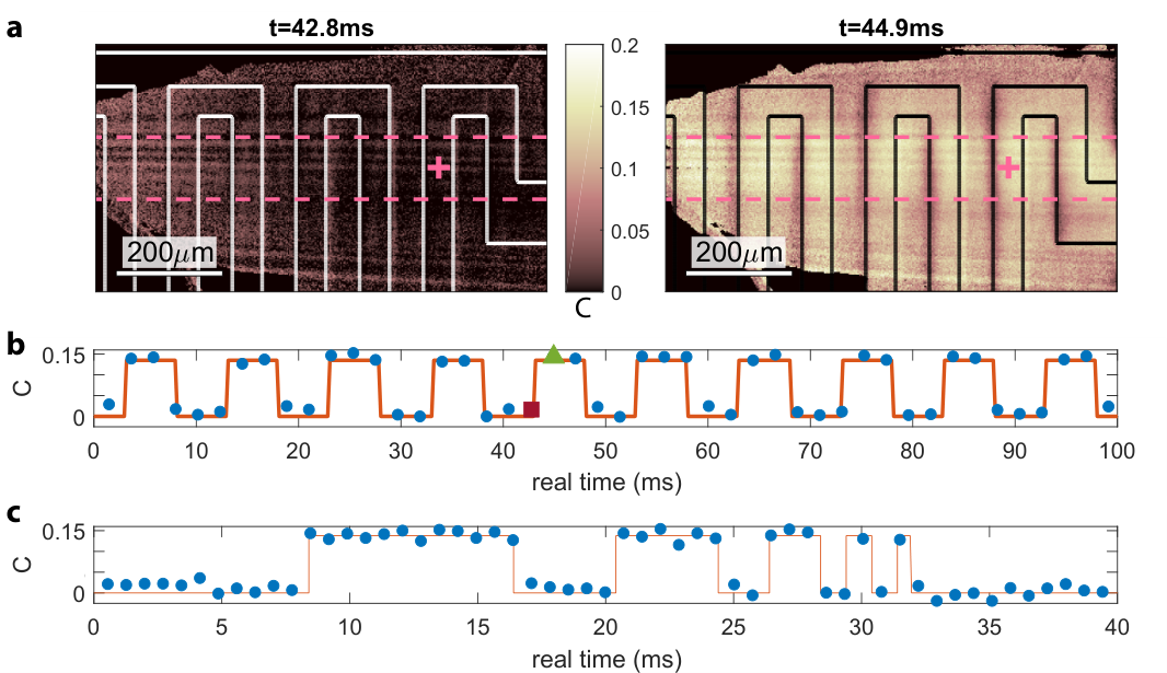
We achieve our highest temporal resolution in the iso-B-field imaging mode, with reference images taken offline. The temporal resolution in our current system is ultimately limited by the camera frame rate, which is proportional to the number of pixel rows read out. Reading out 360 columns and 200 rows, corresponding to a field of view, and choosing shots/exposure, we achieve a temporal resolution of 2.2 ms. We demonstrate this kHz frame rate in Figs. 5a,b, where we measure a pulse train with a 5 ms on/off cycle. Each pixel in Fig. 5a provides a similar time-trace signal to that shown in Fig. 5b. To explore our ability to detect externally controlled signals, we used an independent pulse generator to switch a P, 2.77 GHz signal. The imaging sequence was identical to the reference image sequence in Fig. 1d, but with a fixed gap between laser pulses of ns. Reducing the readout to 50 rows further improves the temporal resolution to 0.7 ms, as shown in Fig. 5c, where we measure a train of pulses between 8 ms and 0.5 ms in length. The measurements in Fig. 5 used a short sensing time, of dt. However, longer sensing periods (e.g. 110s), which would provide images with richer contour lines, can be used without loss of temporal resolution, as the frame rate was dominated by camera readout.
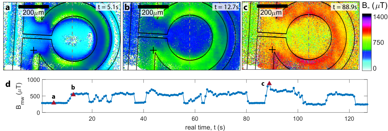
To combine full-B-field imaging with high bandwidth, we performed fast scans of dtmw, with an experiment sequence identical to that used for the images in Figs. 3,4, but with only a single global repeat. There is a tradeoff between temporal resolution and dynamic range, through the choice of number of dtmw steps. We chose a 100-timestep sequence, and performed full-B-field B- imaging with a 1.6 Hz frame rate, using shots/exposure, 200 pixel rows, and with reference images taken online. This imaging mode allows for an intuitive exploration of devices and microwave near fields, as demonstrated in Supplementary Movie 1 [30], where we scan the omega loop chip to explore MW fields upstream of the loop. Figure 6 shows frames and a pixel time-trace from a second movie taken of the omega loop chip (Supplementary Movie 2 [30]), where we deliberately perturbed the microwave current modes by periodically shorting the signal and ground pins of the MW input port. We see the MW amplitude and spatial mode change dramatically, as we change the spatial mode and efficiency of microwave launch into the device. Figures 6b,c show improved MW field homogeneity and strength in the center of the omega loop, compared to the unperturbed case in Fig. 6a (see also profiles of the fields in Supplementary Fig. S8 [30]). This highlights a perhaps rarely considered degree of freedom in experimentally optimising devices, where one could envisage, for example, optimising a device for manipulating quantum systems by shorting the input port pins in a controlled manner.
IV Conclusions and Outlook
We have presented a widefield diamond microscope based on NV centers, and demonstrated its substantial potential for characterizing MW devices. Our sub-millisecond temporal resolution represents an order of magnitude improvement over the previous 10 ms state of the art for diamond microscopes. Our microscope provides intrinsically calibrated, polarization-resolved MW field images, with sensitivity, 48 dB dynamic range, and few-micron spatial resolution over a FOV. In this work, we have performed MW field imaging around 2.77-2.97 GHz, however larger dc magnetic fields can be applied to tune the imaging frequency up to hundreds of GHz [16, 39, 40]. With the addition of a control MW field to perform dynamic decoupling, weak MW fields could be detected up to the limit [41, 42]. With delta-doped NV surface layers, the spatial resolution could be further extended to the sub-micron range [24], or superresolution techniques could be employed to provide resolution down to the nanoscale [43, 44]. We have also identified ways to improve our fluorescence count rate, and thus signal to noise ratio, by over 5 orders of magnitude (see Supplementary Note 1 [30]).
Potential further applications of our high temporal resolution microscope include studies of MW device failure, changes in MW device operation with duty cycle, and monitoring integrated circuitry activity, e.g. logic processes on processor chips [45, 22]. With the addition of a dc magnetic field gradient, our microscope could operate as an analogue MW spectrum analyser [46], providing feedback on sub-ms timescales. MW electric field imaging could be explored, detecting the electric field via Rabi oscillations driven on the electric transition coupling the states [47], with a dc magnetic field used to tune the state splitting to resonance with the MW field. Widefield diamond microscopes hold promise for extending sub-micron widefield microscopy to MW medical imaging [8, 9, 11], which could enable new applications on the cellular level. With the use of a control MW field, materials analysis using scanning MW microscopy [10] could be extended to widefield imaging applications.
In addition to MW field imaging, there are a number of further modalities in which our microscope can be employed, including imaging spin waves in solid state systems [6, 7] to investigate e.g. spin transport waveguides based on ferromagnetic domain walls [48] and as a possible alternative to Brillouin light scattering techniques [49]. Using our 0.7 ms resolution, 2-point differential dc magnetic field imaging can be performed at a 700 Hz rate. This is of interest e.g. for monitoring biological processes such as neuron firing [50] and magnetic nanoparticle formation [51], and for microfluidics applications [52, 53].
Acknowledgments: This work was supported by the Swiss National Science Foundation (SNFS) and DIADEMS. We thank B. Shields, J. Wood, L. Thiel, and M. Ganzhorn for laboratory help and general advice on NV centers, A. Edmonds and M. Markham for providing the (113)-oriented substrates used for CVD overgrowth, G. Witz and T. Julou for help with Micro-Manager, and M. W. Doherty for careful reading of the manuscript.
Author contributions: A.H., P.M. and P.T. conceived the project idea. A.H. designed, built, and operated the microscope, with input from P.A. and J.W.. P.A. and A.H. validated experiment measurements with simulations. J.A. and A.T. fabricated the diamond sample. A.H. and P.T. designed the prototype atom chip and other microwave devices. P.M. and P.T. supervised the project. A.H. wrote the manuscript, with input and discussion from all authors.
References
- [1] Björn T. Rosner and Daniel W. Van Der Weide, “High-frequency near-field microscopy,” Review of Scientific Instruments 73, 2505 (2002).
- [2] Selahattin Sayil, DV Jr. Kerns, and SE Kerns, “Comparison of contactless measurement and testing techniques to a all-silicon optical test and characterization method,” IEEE Trans. Instrum. Meas. 54, 2082–2089 (2005).
- [3] Andrew Horsley, “High Resolution Field Imaging with Atomic Vapor Cells,” PhD Thesis, Department of Physics, University of Basel, Switzerland (2015).
- [4] B Deutschmann, “On the effects of transient electromagnetic interference on integrated circuits,” Electronic Device Failure Analysis 8, 16–24 (2006).
- [5] Tristan Dubois, Sylvie Jarrix, Annick Penarier, Philippe Nouvel, Daniel Gasquet, Laurnet Chusseau, and Bruno Azais, “Near-field electromagnetic characterization and perturbation of logic circuits,” IEEE Trans. Instrum. Meas. 57, 2398–2404 (2008).
- [6] Toeno van der Sar, Francesco Casola, Ronald Walsworth, and Amir Yacoby, “Nanometre-scale probing of spin waves using single-electron spins.” Nature communications 6, 7886 (2015), 1410.6423 .
- [7] Chunhui Du, Toeno Van der Sar, Tony X. Zhou, Pramey Upadhyaya, Francesco Casola, Huiliang Zhang, Mehmet C. Onbasli, Caroline A. Ross, Ronald L. Walsworth, Yaroslav Tserkovnyak, and Amir Yacoby, “Control and Local Measurement of the Spin Chemical Potential in a Magnetic Insulator,” Science 357, 195–198 (2017).
- [8] Natalia Nikolova, “Microwave Imaging for Breast Cancer,” IEEE Microwave Magazine 12, 78–94 (2011).
- [9] Rohit Chandra, Huiyuan Zhou, Ilangko Balasingham, and Ram M Narayanan, “On the Opportunities and Challenges in Microwave Medical Sensing and Imaging,” IEEE Trans. Biomed. Eng. 62, 1667–1682 (2015).
- [10] C. Plassard, E. Bourillot, J. Rossignol, Y. Lacroute, E. Lepleux, L. Pacheco, and E. Lesniewska, “Detection of defects buried in metallic samples by scanning microwave microscopy,” Physical Review B - Condensed Matter and Materials Physics 83, 2–5 (2011).
- [11] Alexander Tselev, Jeyavel Velmurugan, Anton V. Ievlev, Sergei V. Kalinin, and Andrei Kolmakov, “Seeing through Walls at the Nanoscale: Microwave Microscopy of Enclosed Objects and Processes in Liquids,” ACS Nano 10, 3562–3570 (2016).
- [12] Pascal Böhi and Philipp Treutlein, “Simple microwave field imaging technique using hot atomic vapor cells,” Appl. Phys. Lett. 101, 181107 (2012).
- [13] Andrew Horsley, Guan-Xiang Du, Matthieu Pellaton, Christoph Affolderbach, Gaetano Mileti, and Philipp Treutlein, “Imaging of relaxation times and microwave field strength in a microfabricated vapor cell,” Phys. Rev. A 88, 063407 (2013).
- [14] Christoph Affolderbach, Guan-Xiang Du, Thejesh Bandi, Andrew Horsley, Philipp Treutlein, and Gaetano Mileti, “Imaging Microwave and DC Magnetic Fields in a Vapor-Cell Rb Atomic Clock,” IEEE Trans. Instrum. Meas. 64, 3629–3637 (2015).
- [15] Andrew Horsley, Guan-Xiang Du, and Philipp Treutlein, “Widefield microwave imaging in alkali vapor cells with sub-100 m resolution,” New J. Phys. 17, 112002 (2015).
- [16] Andrew Horsley and Philipp Treutlein, “Frequency-Tunable Microwave Field Detection in an Atomic Vapor Cell,” Applied Physics Letters 108, 211102 (2016), 1604.05526 .
- [17] Haoquan Fan, Santosh Kumar, Jonathon Sedlacek, Harald Kübler, Shaya Karimkashi, and James P Shaffer, “Atom based RF electric field sensing,” J. Phys. B 48, 202001 (2015).
- [18] Christopher L. Holloway, Matthew T. Simons, Joshua A. Gordon, Perry F. Wilson, Caitlyn M. Cooke, David A. Anderson, and Georg Raithel, “Atom-Based RF Electric Field Metrology: From Self-Calibrated Measurements to Subwavelength and Near-Field Imaging,” IEEE Transactions on Electromagnetic Compatibility 59, 717–728 (2017).
- [19] C G Wade, N Šibalic, N R de Melo, J M Kondo, C S Adams, and K J Weatherill, “Real-time near- field terahertz imaging with atomic optical fluorescence,” Nature Photonics 11, 40–43 (2017).
- [20] Pengfei Wang, Zhenheng Yuan, Pu Huang, Xing Rong, Mengqi Wang, Xiangkun Xu, Changkui Duan, Chenyong Ju, Fazhan Shi, and Jiangfeng Du, “High-resolution vector microwave magnetometry based on solid-state spins in diamond,” Nat. Commun. 6, 6631 (2015).
- [21] Patrick Appel, Marc Ganzhorn, Elke Neu, and Patrick Maletinsky, “Nanoscale microwave imaging with a single electron spin in diamond,” New J. Phys. 17, 112001 (2015).
- [22] Linbo Shao, Ruishan Liu, Mian Zhang, Anna V. Shneidman, Xavier Audier, Matthew Markham, Harpreet Dhillon, Daniel J. Twitchen, Yun-Feng Xiao, and Marko Lončar, “Wide-Field Optical Microscopy of Microwave Fields Using Nitrogen-Vacancy Centers in Diamonds,” Advanced Optical Materials 4, 1075–1080 (2016).
- [23] K. Chang, A. Eichler, J. Rhensius, L. Lorenzelli, and C. L. Degen, “Nanoscale Imaging of Current Density with a Single-Spin Magnetometer,” Nano Letters 17, 2367–2373 (2017).
- [24] S. Steinert, F. Dolde, P. Neumann, A. Aird, B. Naydenov, G. Balasubramanian, F. Jelezko, and J. Wrachtrup, “High sensitivity magnetic imaging using an array of spins in diamond,” Review of Scientific Instruments 81, 043705 (2010).
- [25] David R Glenn, Kyungheon Lee, Hongkun Park, Ralph Weissleder, Amir Yacoby, Mikhail D Lukin, Hakho Lee, Ronald L Walsworth, and Colin B Connolly, “Single-cell magnetic imaging using a quantum diamond microscope,” Nature Methods 12, 736–738 (2015).
- [26] D A Simpson, J P Tetienne, J M McCoey, K Ganesan, L T Hall, S Petrou, R E Scholten, and L C Hollenberg, “Magneto-optical imaging of thin magnetic films using spins in diamond,” Sci Rep 6, 22797 (2016).
- [27] D. R. Glenn, R. R. Fu, P. Kehayias, D. Le Sage, E. A. Lima, B. P. Weiss, and R. L. Walsworth, “Micrometer-scale magnetic imaging of geological samples using a quantum diamond microscope,” Geochemistry, Geophysics, Geosystems 18, 3254––3267 (2017).
- [28] Jean-Philippe Tetienne, Nikolai Dontschuk, David A. Broadway, Alastair Stacey, David A. Simpson, and Lloyd C. L. Hollenberg, “Quantum imaging of current flow in graphene,” Science Advances 3, e1602429 (2017).
- [29] Patrick Appel, Elke Neu, Marc Ganzhorn, Arne Barfuss, Marietta Batzer, Micha Gratz, Andreas Tschöpe, and Patrick Maletinsky, “Fabrication of all diamond scanning probes for nanoscale magnetometry,” Review of Scientific Instruments 87, 063703 (2016).
- [30] See supplementary material at [link] for further details of the experiment and data analysis, and for movies of microwave magnetic fields captured by our microscope.
- [31] M. Lesik, T. Plays, A. Tallaire, J. Achard, O. Brinza, L. William, M. Chipaux, L. Toraille, T. Debuisschert, A. Gicquel, J. F. Roch, and V. Jacques, “Preferential orientation of NV defects in CVD diamond films grown on (113)-oriented substrates,” Diamond and Related Materials 56, 47–53 (2015).
- [32] Marcus W. Doherty, Neil B. Manson, Paul Delaney, Fedor Jelezko, Jörg Wrachtrup, and Lloyd C.L. Hollenberg, “The nitrogen-vacancy colour centre in diamond,” Physics Reports 528, 1–45 (2013).
- [33] C. L. Degen, F. Reinhard, and P. Cappellaro, “Quantum sensing,” Reviews of Modern Physics 89, 035002 (2017).
- [34] Pascal Böhi, Max F. Riedel, Theodor W. Hänsch, and Philipp Treutlein, “Imaging of microwave fields using ultracold atoms,” Appl. Phys. Lett. 97, 051101 (2010).
- [35] K. Sasaki, Y. Mannai, S. Saijo, R. Fujita, H. Watanabe, J. Ishi-Hayase, K. Itoh, and E. Abe, “Broadband, large-area microwave antenna for optically detected magnetic resonance of nitrogen-vacancy centers in diamond,” Review of Scientific Instruments 87, 053904 (2016).
- [36] Jakob Reichel and Vladan Vuletic, eds., Atom Chips (Wiley-Blackwell VCH, Weihheim, Germany, 2011).
- [37] R. J C Spreeuw, C. Gerz, Lori S. Goldner, W. D. Phillips, S. L. Rolston, C. I. Westbrook, M. W. Reynolds, and Isaac F. Silvera, “Demonstration of neutral atom trapping with microwaves,” Physical Review Letters 72, 3162–3165 (1994).
- [38] Pascal Böhi, Max F. Riedel, Johannes Hoffrogge, Jakob Reichel, Theodor W. Hänsch, and Philipp Treutlein, “Coherent manipulation of Bose-Einstein condensates with state-dependent microwave potentials on an atom chip,” Nature Physics 5, 592–597 (2009).
- [39] Viktor Stepanov, Franklin H. Cho, Chathuranga Abeywardana, and Susumu Takahashi, “High-frequency and high-field optically detected magnetic resonance of nitrogen-vacancy centers in diamond,” Applied Physics Letters 106, 063111 (2015).
- [40] Nabeel Aslam, Matthias Pfender, Rainer Stöhr, Philipp Neumann, Marc Scheffler, Hitoshi Sumiya, Hiroshi Abe, Shinobu Onoda, Takeshi Ohshima, Junichi Isoya, and Jörg Wrachtrup, “Single spin optically detected magnetic resonance with 60-90 GHz (E-band) microwave resonators,” Review of Scientific Instruments 86, 064704 (2015).
- [41] T Joas, A M Waeber, G Braunbeck, and F Reinhard, “Quantum sensing of weak radio-frequency signals by pulsed Mollow absorption spectroscopy,” Nature Communications 8, 964 (2017).
- [42] Alexander Stark, Nati Aharon, Thomas Unden, Daniel Louzon, Alexander Huck, Alex Retzker, Ulrik Lund Andersen, and Fedor Jelezko, “Narrow-bandwidth sensing of high-frequency fields with continuous dynamical decoupling,” Nature Communications 8, 1105 (2017).
- [43] Edward H Chen, Ophir Gaathon, Matthew E Trusheim, and Dirk Englund, “Wide-Field Multispectral Super-Resolution Imaging Using Spin- Dependent Fluorescence in Nanodiamonds,” Nano Letters 13, 2073–2077 (2013).
- [44] K Arai, C Belthangady, H Zhang, N Bar-Gill, S J DeVience, P Cappellaro, A Yacoby, and R L Walsworth, “Fourier magnetic imaging with nanoscale resolution and compressed sensing speed-up using electronic spins in diamond,” Nature Nanotechnology 10, 859–864 (2015).
- [45] A. Nowodzinski, M. Chipaux, L. Toraille, V. Jacques, J. F. Roch, and T. Debuisschert, “Nitrogen-Vacancy centers in diamond for current imaging at the redistributive layer level of Integrated Circuits,” Microelectronics Reliability 55, 1549–1553 (2015).
- [46] M. Chipaux, L. Toraille, C. Larat, L. Morvan, S. Pezzagna, J. Meijer, and T. Debuisschert, “Wide bandwidth instantaneous radio frequency spectrum analyzer based on nitrogen vacancy centers in diamond,” Applied Physics Letters 107, 233502 (2015).
- [47] A. Barfuss, J. Teissier, E. Neu, A. Nunnenkamp, and P. Maletinsky, “Strong mechanical driving of a single electron spin,” Nature Physics 11, 820–824 (2015).
- [48] Felipe Garcia-Sanchez, Pablo Borys, Rémy Soucaille, Jean-paul Adam, Robert L Stamps, and Joo Von Kim, “Narrow Magnonic Waveguides Based on Domain Walls,” Phys. Rev. Lett. 114, 247206 (2015).
- [49] Thomas Sebastian, Katrin Schultheiss, Björn Obry, Burkard Hillebrands, and Helmut Schultheiss, “Micro-focused Brillouin light scattering: imaging spin waves at the nanoscale,” Frontiers in Physics 3, 35 (2015).
- [50] L T Hall, G C G Beart, E A Thomas, D A Simpson, L P McGuinness, J H Cole, J H Manton, R E Scholten, F Jelezko, Jörg Wrachtrup, S Petrou, and L C L Hollenberg, “High spatial and temporal resolution wide-field imaging of neuron activity using quantum NV-diamond.” Scientific Reports 2, 401 (2012).
- [51] D Le Sage, K Arai, D R Glenn, S J DeVience, L M Pham, L Rahn-Lee, M D Lukin, A Yacoby, A Komeili, and R L Walsworth, “Optical magnetic imaging of living cells.” Nature 496, 486–9 (2013).
- [52] Li Yao and Shoujun Xu, “Detection of magnetic nanomaterials in molecular imaging and diagnosis applications,” Nanotechnology Reviews 3, 247–268 (2014).
- [53] D Issadore, Y I Park, H Shao, C Min, K Lee, M Liong, R Weissleder, and H Lee, “Magnetic sensing technology for molecular analyses.” Lab on a Chip 14, 2385–97 (2014).
- [54] Michael S.J. Barson, Phani Peddibhotla, Preeti Ovartchaiyapong, Kumaravelu Ganesan, Richard L. Taylor, Matthew Gebert, Zoe Mielens, Berndt Koslowski, David A. Simpson, Liam P. McGuinness, Jeffrey McCallum, Steven Prawer, Shinobu Onoda, Takeshi Ohshima, Ania C. Bleszynski Jayich, Fedor Jelezko, Neil B. Manson, and Marcus W. Doherty, “Nanomechanical Sensing Using Spins in Diamond,” Nano Letters 17, 1496–1503 (2017).
- [55] Bradley J Roth, Nestor G Sepulveda, and John P Wikswo Jr, “Using a magnetometer to image a twodimensional current distribution,” Journal of Applied Physics 65, 361 (1989).
- [56] D Budker and M Romalis, “Optical magnetometry,” Nature Physics 3, 227–234 (2007).
- [57] Nico Stuurman, Arthur D Edelstein, Nenad Amodaj, Karl H Hoover, and D Ronald, “Computer Control of Microscopes using Manager,” Current Protocols in Molecular Biology , 92:14.20:14.20.1 14.20.17 (2010).
- [58] Arthur D Edelstein, Mark A Tsuchida, Nenad Amodaj, Henry Pinkard, Ronald D Vale, and Nico Stuurman, “Advanced methods of microscope control using Manager software,” Journal of Biological Methods 1, 10 (2014).
- [59] Hannah Clevenson, Matthew E Trusheim, Tim Schröder, Carson Teale, Danielle Braje, and Dirk Englund, “Broadband magnetometry and temperature sensing with a light trapping diamond waveguide,” Nature Physics 11, 393–397 (2015).
- [60] R. Hanson, V. V. Dobrovitski, A. E. Feiguin, O. Gywat, and D. D. Awschalom, “Coherent Dynamics of a Single Spin Interacting with an Adjustable Spin Bath,” Science 320, 352–356 (2008).
- [61] A. Dréau, M. Lesik, L. Rondin, P. Spinicelli, O. Arcizet, J. F. Roch, and V. Jacques, “Avoiding power broadening in optically detected magnetic resonance of single NV defects for enhanced dc magnetic field sensitivity,” Physical Review B 84, 195204 (2011).
- [62] Rich Mildren and James Rabeau, eds., Optical Engineering of Diamond (Wiley-VCH, Weihheim, Germany, 2013).
- [63] Jacques Vanier, Claude Audoin, and Adam Hilger, The Quantum Physics of Atomic Frequency Standards, Vol. 1 (Adam Hilger, Bristol, 1989).