RESEARCH PAPER \Year2018 \MonthJanuary \Vol61 \No1 \DOI \ArtNo \ReceiveDate \ReviseDate \AcceptDate \OnlineDate
Polar FEC for NAND flash memory
chzhang@seu.edu.cn
Song H
Song H, Fu F, Zeng C, Sha J, Zhang Z, You X, Zhang C
Polar-Coded Forward Error Correction for MLC NAND Flash Memory
Abstract
With the ever-growing storage density, high-speed, and low-cost data access, flash memory has inevitably become popular. Multi-level cell (MLC) NAND flash memory, which can well balance the data density and memory stability, has occupied the largest market share of flash memory. With the aggressive memory scaling, however, the reliability decays sharply owing to multiple interferences. Therefore, the control system should be embedded with a suitable error correction code (ECC) to guarantee the data integrity and accuracy. We proposed the pre-check scheme which is a multi-strategy polar code scheme to strike a balance between reasonable frame error rate (FER) and decoding latency. Three decoders namely binary-input, quantized-soft, and pure-soft decoders are embedded in this scheme. Since the calculation of soft log-likelihood ratio (LLR) inputs needs multiple sensing operations and optional quantization boundaries, a -bit quantized hard-decision decoder is proposed to outperform the hard-decoded LDPC bit-flipping decoder with fewer sensing operations. We notice that polar codes have much lower computational complexity compared to LDPC codes. The stepwise maximum mutual information (SMMI) scheme is also proposed to obtain overlapped boundaries without exhausting search. The mapping scheme using Gray code is employed and proved to achieve better raw error performance compared to other alternatives. Hardware architectures are also given in this paper.
keywords
Polar coding, non-volatile memory, error correcting code, NAND, flash memory1 Introduction
Nowadays, the ever-developing digital technologies enable us to achieve extremely high communication speed. However, traditional hard disk drive (HDD) can no longer meet the throughput and latency requirements of most state-of-the-art application scenarios. To this end, NAND flash memory, which is of lower access time, higher compactness, and less noise has become increasingly popular for storage market [1, 2].
The past decade has witnessed the steady price fall of flash memory and is expecting further price-drop in the future [3, 4]. This trend has enabled solid state drive (SSD), which is mainly based on NAND flash memory, to occupy a large share of both business and consumer markets.
1.1 Challenges and motivation
As the required storage density increases, most NAND flashes consider to store bits in a single cell [5, 6, 7, 8], which results in worse raw error performance. Therefore, powerful forward-error correction (FEC) methods are required, and voluminous researches on conventional error correction code (ECC) schemes for NAND flash memory emerge [9, 11, 10, 13, 12]. Recently, low-density parity-check (LDPC) codes have been considered. To balance performance and complexity, hybrid scheme combining hard decoder and soft decoder is always employed. However, the accepted soft decoders such as min-sum and belief-propagation (BP) suffer from high complexity. Identifying an alternative code might serve as a solution.
Recently, polar codes [14] have shown capacity-achieving performance and reasonable complexity [15, 16]. Besides its good performance over binary-input discrete memoryless channels (B-DMCs), -bit polar code’s encoding and decoding complexity is as low as , which is much lower than that of LDPC code. Consequently, polar codes have been selected as the control channel code for the enhanced mobile broadband (eMBB) scenario by 3GPP [17]. Inspired by few existing literature [18], this paper devotes itself in proposing an efficient polar-coded forward error correction for multi-level cell (MLC) NAND flash memory.
1.2 Contributions
To balance the performance and delay, this paper proposes a pre-check scheme based on polar code for MLC NAND flash. Our main contributions are notably:
- •
We propose the pre-check scheme to arrange pure-soft, quantized-soft, and binary-input polar decoders in different life-stages of SSD.
- •
We have proved that polar code is a balanced code for which each codeword contains an equal
number of zero and one bits. - •
We propose a well-designed hard-decision binary-input polar decoder. This decoder directly employs -bit hard results returned from the voltage detector and utilizes a single XOR gate to calculate
log-likelihood ratios (LLRs). - •
We compare the complexities of binary-input SC polar decoder, SC polar decoder, binary-input bit-flipping LDPC decoder, and layered BP polar decoder. Results show that binary-input SC polar decoder has the lowest complexity given a target error performance. Besides, it also has better performance than traditional hard-decision bit-flipping LDPC decoder.
- •
We propose a new quantized-soft polar decoder with refined boundary-defining scheme to improve the empirical method.
- •
We clarify that Gray code is the optimal scheme to map bits in cell.
1.3 Notations
Let and designate likelihood ratio (LR) and LLR, respectively. Sets are denoted by uppercase calligraphic letters as . We indicate the probability density function (PDF) of a voltage distribution by . The uppercase letter designates probability cumulated by PDFs. The entropy function is .
1.4 Paper outline
The remainder of this paper is organized as follows. Section 2 reviews background of NAND flash and polar codes. Section 3 proposes the Gray mapping scheme and pre-check scheme. Three polar decoders are discussed in this section too. In Section 4, hardware architecture of proposed binary-input decoder is detailed. In Section 5, performance and complexity are compared for different decoders. Finally, Section 6 concludes this paper. Proof for Gray mapping scheme and the correction of previous work [11] are presented in Appendix.
2 Background of MLC NAND flash memory and polar codes
2.1 Modeling of NAND flash memory
Floating gate transistors constitute the NAND flash memory [1]. Programming is an operation which stepwise injects a certain quantity of charges to achieve a target voltage. Unavoidably influenced by multiple interferences, voltages will turn into wide ranges, which results in overlapped regions.
The voltage distribution adopted in this work originates from [20]. Gaussian distribution is selected for both convenience and accuracy of modeling [21].
For design purposes, each cell is initialized with distributions away from each other. However, these distributions gets closer with increasing program/erase (P/E) cycles and multiple interferences. Raw error happens when overlapped regions exist.
2.2 Basics of polar codes
Proposed by E. Arıkan in [14], polar codes have the capability of achieving the symmetric capacity of any given B-DMC , so long as the code length goes to infinity. To better understand polar codes, LLR-based min-sum SC decoding algorithm [19] is introduced below.
In an arbitrary code with parameter , code length and information length are represented by and . Source vector, the input vector of SC encoder, is denoted by , which consists of an information part and a frozen part . Note that frozen bits are usually set to .
The LLR-based min-sum SC decoding algorithm is defined as
| (1) |
| (2) | ||||
The hardware architecture of this algorithm is explained in [16].
3 Multi-strategy ECC scheme
In this section, we first demonstrate the adopted Gray mapping scheme. Then we propose the pre-check scheme with multi-strategy ECC and corresponding polar decoders.
3.1 Gray mapping and detection
The programmed symbols for each state of MLC NAND flash memory are shown in Figure 2. Note that a raw error happens when a state is mistakenly considered for its neighboring states. Moreover, and have -bit difference under direct mapping. Hence, we should consider a mapping scheme that is capable of reducing raw error bits. To this end, Gray mapping with minimum difference between adjacent states is the optimal choice. The proof is shown in A.


3.2 Control system
The overall architecture of error correction module is illustrated in Figure 2. Polar decoder will encode the external bit stream into binary codewords. Then these codewords will be pairwise mapped to a certain voltage in each cell. To recover the stored data, the detector first senses a cell several times and compare the stored voltage to reference voltages. After that, pre-check scheme will determine which decoder should be picked and then process the comparison results to LLRs to feed corresponding decoders.


Figure 4 illustrates the flow of each step in the pre-check scheme. Cell state will be checked at the beginning to determine which decoder should be picked. When cell distortion appears slight, the binary-input decoder is chosen owing to its low decoding latency. When distortion is getting worse, soft-decision decoders should be selected to guarantee data integrity.
3.3 Pre-check scheme
This scheme aims to select an optimal decoder in accordance of the condition to meet the demand for storage reliability.
Assume the mean values of four states are , , , and respectively and the standard deviation is , which is identical for all distributions.
The cell state can be expressed as a set of equations as
| (5) |
By solving (6)
| (6) |
we can obtain intersections between distributions which are
Since mean values are uniformly distributed and standard deviations are identical, reference voltage is the mid-value between and . A raw error will occur when the sensed voltage gets across the reference voltage. For example, if a voltage of state is greater than , it is more likely to be considered as a voltage in (i.e., an error happens). Therefore, we can calculate the raw error probability for each overlapped region by
| (7) |
is a function of variable , where is the distance between two adjacent distributions and is the standard deviation. In NAND flash memory, the values of and change over time due to voltage shifting and cell distortion. Since is monotonically decreasing with and is decreasing over time (the experiment in [21] has shown that the signal-to-noise ratio (SNR) in the NAND flash memory degrades about dB per k P/E cycles), the value of is increasing.
With numerical , we can set several thresholds to adjust the decoding scheme to satisfy performance requirements of the system.
3.4 Pure-soft decoder
The sensed voltage needs to be converted into digital LLR to feed the pure-soft decoder.
Given the model of NAND flash memory in Section 2, the whole voltage range can be described with Gaussian distributions indicated by , and . To obtain the definition of LLR in NAND flash memory, there are some basic ideas that need to be clarified.
[]
Polar code is a balanced code for which each codeword contains an equal number of zero and one bits.
Proof.
The codeword and the -th element of are constructed as
where is the source information, is the generator matrix and denotes the -th column of .
With the property of multiplication in , whether is or is only determined by the number of ’s in whose corresponding places in are . For example, if , then we have
| (8) |
Since some elements in are , only a part of elements in participate in the calculation. In the example of (8), only and are concerned.
Assume that the number of ’s in is . The probability for being or can be denoted by
Lemma 3.4 is the foundation for LLR calculation in NAND flash memory. This a priori property guarantees the usage of Bayes Law within LLR calculation for all the polar decoders discussed in this paper.
[] For any stored bit , its LLR is defined as
| (9) |
where denotes the -th PDF of voltage distribution, denotes the sensed voltage, contains distributions where and contains distributions where .
Proof.
According to the definition, the LLR of should be denoted by
| (10) |
However, considering the difficulty of directly acquiring the a posteriori probability , it is simple to transform (10) into the form of likelihood function according to the Bayes theorem as
| (11) |
where , according to Lemma 3.4, and is the summation of PDFs when is settled. Therefore, the LLR of is exactly the form in (9). Note that and are different according to the adopted mapping scheme. An example is shown in Figure 6.


3.5 Quantized-soft decoder
The LLR calculation mentioned in Section 3.4 can achieve the best performance of error correction. However, it requires an accurate value of the sensed voltage, which is unrealistic in circuits. Therefore, a proper scheme which can balance the numerical accuracy and sensing latency is highly needed.
3.5.1 Problems in quantized-soft decoder
The main constrain is that the detector can only return a comparison result between the sensed voltage and pre-set references which we call “hard result”, containing only -bit information.
This raises two problems. The first one is obtaining proper references (or boundaries). The definition of overlapped regions is crucial to calculate LLRs.
3.5.2 Boundaries defined by constant ratio
In our previous work [22], we adopted the boundary-defining scheme that was proposed in [10] and expanded in [11]. In this section, we show the basic idea in [10] and the re-derived quadratic equation set which differs from the equations in [11].
and are boundaries restricting the th region, and is a pre-settled ratio. The relation among , and is as
| (12) |
where is the th voltage distribution. Under Gaussian estimation, this calculation is significantly simplified compare with [10].
3.5.3 Boundaries defined by stepwise mutual information
The boundary-defining scheme of constant ratio mentioned in Section 3.5.2 is effective to locate the overlapped regions. However, there still remains an unsolved problem that the value of is mostly determined by empirical evidence.
A different scheme called maximum mutual information (MMI) is proposed in [23] which aims to set quantization boundaries that maximize the mutual information. MMI quantizes the whole voltage range into regions with sensing operations.
However, MMI is a general case instead of an optimal choice for boundary selection because the mutual information defined in [23] is calculated for each region instead of original bits, whereas LLRs are calculated bitwise. In this work, we calculate mutual information for the most significant bit (MSB) and the least significant bit (LSB) separately, which we call stepwise mutual information (SMMI).
Figure 8 shows the relationship between reference voltages and mapped bits. It is obvious that the judgement of the LSB only relates to quantization boundaries and . Similarly, , and are responsible for sensing operation of the MSB. We take the LSB as an example to demonstrate the channel and the entropy calculation under SMMI strategy.

MLC model for MMI scheme.


In Figure 10, the whole range is separated into quantized regions, hence this quantization model is equivalent to a -input, -output channel model with and given in Figure 10, which is similar to the model of single-level cell (SLC) NAND flash memory with reads in [24].
According to Lemma 3.4, sends and under equal probability. Therefore, the mutual information between and is calculated as
| (14) |
For a settled voltage distribution, the mutual information between and can be numerically maximized to obtain desired boundaries and that yield the SMMI.
3.5.4 Practical SMMI boundary calculation
In the MMI example shown above, a input, output MLC model shown in Figure 8 was adopted for illustration purposes. However, there are at least sensing operations in overlapped region in a practical control system as demonstrated in Figure 11, where the intersections of two distributions in the middle are called “hard-decision boundaries” and mentioned before are called “soft-decision boundaries”. Channel models for the LSB and the MSB in this scheme are shown in Figure 13 and Figure 13.


The mutual information for the LSB in this case is calculated as
| (15) | ||||
and the mutual information for the MSB is calculated as
| (16) | ||||
3.5.5 LLR calculation
According to (9), quantized LLRs are calculated as follows:
| (17) |
and designate LLRs of the LSB and the MSB of the quantization region . We take the LSB as an example to further explain (17).
Under Gray mapping scheme in Section 3.1 (illustrated in Figure 14), and are distributions where LSB. Meanwhile, and are distributions where LSB. Under this condition, the numerator in (17) which contains the integral with respect to of PDF over the interval represents the probability for LSB. In this way, the denominator is the probability where LSB.
Under Gaussian estimation, -function can easily calculate desired LLRs as
| (18) |
3.6 Binary-input decoder
A sensing strategy is shown in Figure 14. Three reference voltages are denoted by , , and which separate voltage distributions. The detector first compare current voltage with to decide the LSB and then with or to decide the MSB. Detailed description can be found in [22].

According to (4), is judged by the sign bit of LLR. Therefore, hard results can be fully utilized since they can represent the sign bit of LLR. In other words, they can be transformed into a special form of quantized LLR consisting of only a sign bit, for which it is called “binary-input decoder”.
Magnitude of LLR is not concerned in this scenario and only sign bits will participate in the subsequent calculation, which makes it possible to apply simple bit operations in hardware without adder-subtractors in traditional processing element (PE) design [15]. This design is hardware-friendly and will be further discussed in Section 4.
4 Architecture of proposed binary-input decoders
4.1 Two’s complement analysis
According to (1), Type I PE will result in if LLRs are quantized to . In other words, data transferred between entities in different levels are not completely in binary form and hence can not be represented by a single bit. Therefore, -bit ’s complement is adopted for simplicity of logical functions and demand of indicating possible LLRs .
4.2 Input and output analysis
4.2.1 Type I PE
According to [15], universal Type I PE based on min-sum SC algorithm is a series of half or full adder-subtractors. Calculation of LLRs in (1) is significantly simplified under -bit quantization.
Unlike universal Type I PE calculation with arbitrary inputs, binary PE has a limited input set which exhaustively lists all possible results. Suppose and are two -bit operands, is the last decoded bit which chooses the calculation pattern, and is the output. The mathematical function of Type I PE is
| (19) |
| u | X | Y | Z |
| 0 | -1 | -1 | |
| 0 | -1 | 0 | -1 |
| 0 | -1 | 1 | 0 |
| 0 | 0 | -1 | -1 |
| 0 | 0 | 0 | 0 |
| 0 | 0 | 1 | 1 |
| 0 | 1 | -1 | 0 |
| 0 | 1 | 0 | 1 |
| 0 | 1 | 1 | |
| 1 | -1 | -1 | 0 |
| 1 | -1 | 0 | 1 |
| 1 | -1 | 1 | |
| 1 | 0 | -1 | -1 |
| 1 | 0 | 0 | 0 |
| 1 | 0 | 1 | 1 |
| 1 | 1 | -1 | |
| 1 | 1 | 0 | -1 |
| 1 | 1 | 1 | 0 |
| u | X | Y | Z |
|---|---|---|---|
| 0 | 11 | 11 | 11 |
| 0 | 11 | 00 | 11 |
| 0 | 11 | 01 | 00 |
| 0 | 00 | 11 | 11 |
| 0 | 00 | 00 | 00 |
| 0 | 00 | 01 | 01 |
| 0 | 01 | 11 | 00 |
| 0 | 01 | 00 | 01 |
| 0 | 01 | 01 | 01 |
| 1 | 11 | 11 | 00 |
| 1 | 11 | 00 | 01 |
| 1 | 11 | 01 | 01 |
| 1 | 00 | 11 | 11 |
| 1 | 00 | 00 | 00 |
| 1 | 00 | 01 | 01 |
| 1 | 01 | 11 | 11 |
| 1 | 01 | 00 | 11 |
| 1 | 01 | 01 | 00 |
Note that the results of (19) may be and will be quantized to for simplicity of calculation. Therefore, all the possible results are listed in Table 2 and we can directly focus on the input and output by transforming Table 2 into ’s complement as shown in Table 2 instead of messing with those intermediate results like or . In particular, we can separate the MSB and the LSB of output and treat this PE as a combinational logic circuit with a -bit input () and a -bit output (). Therefore, Table 2 is the truth table for this logic circuit which enables us to simply build corresponding logic functions.
4.2.2 Type II PE
The architecture of Type II PE is more straightforward. With binary input, (2) can be pruned to
| (20) |
without obtaining the minimum of inputs since their absolute values have already been quantized to .
Considering the property of multiplication, the output will be once there exists a in inputs. Therefore, hardware architecture design can be simplified by independently considering inputs . Note that both ’s complements of have the same LSB as and the outputs can only be , which means the LSB will constantly be . Therefore, we can extract the MSB to analyze the input and output (I/O). I/O analysis and the corresponding ’s complements have been shown in Table 4 and 4 by adopting the method mentioned in Section 4.2.1.
| -1 | -1 | 1 |
| -1 | 1 | -1 |
| 1 | 1 | 1 |
| 1 | -1 | -1 |
| 1 | 1 | 0 |
| 1 | 0 | 1 |
| 0 | 0 | 0 |
| 0 | 1 | 1 |
We can conclude from Table 4 that the calculation of the MSB of Type II PE using ’s complement equals to an XOR operation. Therefore Type II PE can be pruned to an XOR operation in the MSB and a fixed in the LSB.
4.3 Design of binary PEs
4.3.1 Design of binary Type I PE
Binary Type I PE can be treated as a combinational logic circuit based on the analysis in Table 2.
In this part, variable settings in Section 4.2.1 are adopted and therefore and are two binary input operands, the last-decoded bit is a selection bit and the output is represented by . With -bit quantization for and , binary Type I PE consists of inputs () and outputs (). The logical functions are listed as follows:
- •
(21) - •
(22)
The gate-level circuit diagram of binary Type I PE is depicted in Figure 16.


4.3.2 Design of binary Type II PE
The core of Type II PE design can be concluded into key points based on the aforementioned I/O analysis.
- 1)
MSB of Type II PE’s output can be simply calculated by an XOR operation under -bit ’s complement;
- 2)
The LSB of Type II PE’s output is fixed to ;
- 3)
The output will be once there exists a in the inputs.
Architecture of binary Type II PE is shown in Figure 16.
5 Performance assessment
In this section, we provide the error performance of different codes and discuss their complexities.
5.1 Settings of simulation
We adopt a polar codes using different inputs under MLC NAND flash memory channels. Besides, a QC-LDPC code using bit-flipping decoding algorithm is also used for comparison. The selection of information length if based on [25, 26].
We adopt a -bit/cell MLC NAND flash memory model [20] as the simulation environment. It is assumed that the mean value of Gaussian distribution for erase state which represents is volt and the target voltages in programming states are volt, volt, and volt for symbols , , and , respectively. Standard deviations for each state are set to , and , where changes over time due to multiple interferences. Hard-decision boundaries in binary decoder are the intersections between Gaussian distributions, and SMMI is applied to obtain other soft-decision boundaries.
The binary-input decoder employees -bit quantized LLR. Floating-point LLR is used in quantized-soft decoders. The maximum iteration is set to in hard-decision bit-flipping LDPC decoding.
5.2 Simulation
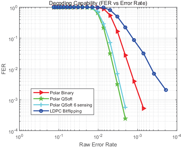
The result is based on FER versus raw error probability and the design of axis is explained as follows. The MLC flash memory is modeled as Gaussian distributions and has hard-decision boundaries. In hard decoding, a raw error happens once the voltage in a Gaussian distribution shifts to its adjacent distributions (i.e., crosses the left or right hard-decision boundary). Under Gaussian distribution, the raw error probability can be calculated by -function.
In Figure 18, binary-input polar decoder obviously outperforms the hard-decision bit-flipping LDPC decoder. With the increment of sensing operations, quantized-soft polar codes is capable of correcting more error bits than binary-input polar code which assures the data stability of the whole system.
5.3 Complexity analysis

different algorithms.
5.3.1 Decoding of polar code
The complexity of full size SC is , where is the code length [14]. For LLR-based min-sum SC decoding, the decoder complexity is:
- •
Type I PEs: additions;
- •
Type II PEs: comparisons/selection (equivalent of addition) and sign bit multiplication (equivalent of XOR);
Overall, the decoding complexity is () additions (XOR is negligible compared to addition).
For binary-input SC decoding, LLRs are quantized to , which means the comparison in Type II PEs is no longer needed. Therefore, the overall decoding complexity is -bit additions and XOR operations.
5.3.2 Decoding of LDPC code
Among various LDPC decoding algorithms, min-sum algorithm is the most widely used method [9, 11, 10, 12]. In this section, we adopt the complexity analysis of LBP decoding with min-sum algorithm in [27]. In this section, code length and information length are represented by and . Column and row weight are denoted by and .
For LBP decoding, the complexity in one iteration is:
- •
Check node processing: additions and comparisons (equivalent of addition);
- •
Variable node processing: additions;
Overall, the decoding complexity is additions per iteration. According to [27], the LBP decoding converges within to iterations (denoted by ) and average column weight (when code rate ). To this end, is obviously smaller than when is less than K byte in storage system. Therefore the computational complexity of SC polar decoding is much lower than LDPC LBP decoding. The complexity of standard BP decoding with min-sum algorithm is similar to this result.
For hard-decision bit-flipping decoding, the complexity in one iteration is:
- •
Syndrome calculation: additions and multiplication in ;
- •
Number of unsatisfied parity checks: additions where is number of ’s in the syndrome;
- •
comparisons (equivalent of additions) to obtain the largest number of unsatisfied parity checks.
The complexity for bit-flipping decoding is mainly determined by the comparisons. Hence the overall decoding complexity is additions in the worst case. In [9], the iteration of modified gradient descent bit-flipping (MGDBF) decoder is set to .
5.3.3 Comparison of decoding complexity
When setting code length as , information length as , iteration as , column weight as , and row weight as , the the decoding complexity is compared in Figure 18. It is obvious that the proposed binary-input SC decoder has the lowest complexity. Moreover, polar codes using SC algorithm have much lower computational complexity compared to traditional LDPC codes using LBP decoding.
6 Conclusion
This paper demonstrates that polar coded scheme holds great promise for data stability of MLC NAND flash memory. The proposed multi-strategy pre-check scheme can well balance the error performance and decoding latency. The binary-input decoder is also proposed to relieve the quantization burden of quantized-soft decoder, and lower the computational complexity compared to LDPC codes. Third, a new method named SMMI is proposed to calculate quantization boundaries without boundary searching. Finally, the Gray code has been proved the optimal mapping scheme in our system.
References
- [1] S. Li, T. Zhang. Improving multi-level NAND flash memory storage reliability using concatenated bch-tcm coding. IEEE Trans. VLSI Syst., 2010, vol. 18, no. 10, pp. 1412–1420,.
- [2] J. Kim, W. Sung. Low-energy error correction of NAND flash memory thourgh soft-decision decoding. EURASIP Journal on Advances in Signal Processing, 2012, vol. 2012.
- [3] LM. Grupp, JD. Davis, S. Swanson. The bleak future of NAND flash memory. In: Proceedings of the 10th USENIX conference on File and Storage Technologies, 2012.
- [4] J. Bellorado, E. Yaakobi. Signal Processing and Coding for Non-Volatile Memories. faculty.cse.tamu.edu/ajiang/NVMW_Tutorial.eps, 2013.
- [5] G. Marotta, A. Macerola, A. D¡¯Alessandro, et al. A 3bit/cell 32Gb NAND flash memory at 34nm with 6MB/s program throughput and with dynamic 2b/cell blocks configuration mode for a program throughput increase up to 13MB/s. In: Solid-State Circuits Conference Digest of Technical Papers (ISSCC), 2010.
- [6] Y. Li, S. Lee, Y. Fong, et al. A 16 Gb 3-bit per cell (X3) NAND flash memory on 56 nm technology with 8 MB/s write rate. IEEE Journal of Solid-State Circuits, 2009, vol. 44(1), pp. 195-¨C207.
- [7] N. Shibata, H Maejima, K. Isobe K, et al. A 70 nm 16 Gb 16-level-cell NAND flash memory. IEEE Journal of Solid-State Circuits, 2008, vol. 43(4), pp. 929¨C-937.
- [8] C. Trinh, N. Shibata, T. Nakano, et al. A 5.6 MB/s 64Gb 4b/cell NAND flash memory in 43nm CMOS. In: Solid-State Circuits Conference-Digest of Technical Papers(ISSCC), 2009.
- [9] K. C. Ho, C. L. Chen, Y. C. Liao, H. C. Chang, and C. Y. Lee, A 3.46 gb/s (9141, 8224) LDPC-based ECC scheme and on-line channel estimation for solid-state drive applications. In: Proceedings of IEEE Int. Symp. Circuits and Systems (ISCAS), Lisbon, Portugal, 2015.
- [10] G. Dong, N. Xie, and T. Zhang, On the use of soft-decision error-correction codes in NAND flash memory. IEEE Trans. Circuits Syst. I, 2011.
- [11] J. Kim, D.-h. Lee, W. Sung. Performance of rate 0.96 (68254, 65536) EG-LDPC code for NAND flash memory error correction. In: Proceedings of IEEE International Conference on Communications (ICC), Ottawa, Canada, 2012.
- [12] Z. Cui, Z. Wang, X. Huang. Multilevel error correction scheme for MLC flash memory. In: IEEE International Symposium on Circuits and Systems (ISCAS), 2014.
- [13] B. Chen, X. Zhang, Z. Wang. Error correction for multi-level NAND flash memory using Reed-Solomon codes. In: Proceedings of IEEE Workshop on Signal Processing Systems (SiPS), 2008.
- [14] E. Arıkan. Channel polarization: A method for constructing capacity-achieving codes for symmetric binary-input memoryless channels. IEEE Trans. Inf. Theory, 2009, vol. 55, no. 7, pp. 3051–3073.
- [15] C. Zhang, B. Yuan, K. K. Parhi. Reduced-latency sc polar decoder architectures. In: Proceedings of IEEE International Conference on Communications (ICC), 2012, pp. 3471–3475.
- [16] C. Zhang, K. K. Parhi. Low-latency sequential and overlapped architectures for successive cancellation polar decoder. IEEE Trans. Signal Process., 2013, vol. 61, no. 10, pp. 2429–2441.
- [17] MCC Support. Final Report of 3GPP TSG RAN WG1 . In: 3GPP TSG WG1 Meeting , www.3gpp.org/ftp/tsg_ran/WG1_RL1/TSGR1_87/Report/, 2016.
- [18] Y. Li, H. Alhussien, E. Haratsch, et al. A study of polar codes for MLC NAND flash memories. International Conference on Computing, NETWORKING and Communications, 2015.
- [19] C. Leroux, I. Tal, A. Vardy, et al. Hardware architectures for successive cancellation decoding of polar codes. In: Proceedings of IEEE International Conference on Acoustics, Speech and Signal Processing (ICASSP), Prague, Czech, 2011, pp. 1665–1668.
- [20] G. Atwood, A. Fazio, D. Mills, B. Reaves. Intel strataflash memory technology overview. Intel Technology Journal, 1997.
- [21] Y. Cai, E. F. Haratsch, O. Mutlu K. Mai. Error patterns in MLC nand flash memory: Measurement, characterization, and analysis. In: Proceedings of Conference on Design, Automation and Test in Europe£¬ 2012, pp. 521–526.
- [22] H. Song, C. Zhang, S. Zhang, et al. Polar code-based error correction code scheme for NAND flash memory applications. In: Proceedings of International Conference on Wireless Communications and Signal Processing (WCSP), 2016.
- [23] J. Wang, T. Courtade, H. Shankar, et al. Soft information for LDPC decoding in flash: mutual-information optimized quantization. In: Proceedings of IEEE Global Telecommunications Conference (GLOBECOM), 2011.
- [24] J. Wang, G. Dong, T. Zhang, et al. Mutual-information optimized quantization for LDPC decoding of accurately modeled flash data. arXiv:1202.1325, 2012.
- [25] N. Mielke, T. Marquart, N. Wu, et al. Bit error rate in nand flash memories. In: Proceedings of IEEE International Reliability Physics Symposium (IRPS), 2008, pp. 9¨C19.
- [26] K. Takeuchi. Novel co-design of nand flash memory and nand flash controller circuits for sub-30 nm low-power high-speed solid-state drives (ssd). IEEE Journal of Solid-State Circuits, vol. 44, no. 4, pp. 1227¨C1234, 2009.
- [27] Y. Blankenship, S. Kuffner. LDPC decoding for 802.22 standard. IEEE P802.22, 2007.
- [28] Q. Xu, Z. Pan, N. Liu, et al. A complexity-reduced fast successive cancellation list decoder for polar codes. Science China Information Sciences, 2018, vol. 61, no.2: pp. 022309.
- [29] Z. Chen, L. Yin, Y. Pei, et al. CodeHop: Physical layer error correction and encryption with LDPC-based code hopping. Science China Information Sciences, 2016, vol. 59, no.10, pp.102309.
Appendix A Proof for Gray code mapping scheme
Gray code can achieve best coding gain compared to any other mapping schemes.
Proof.
As mentioned in Section 3.1, we have noticed that most raw errors happen when a voltage is mistaken for its adjacent levels. Therefore, we can focus on overlapped regions when talking about mapping schemes. For the convenience of discussion, we use column vectors to indicate different states in a -bit memory cell namely , , , . By making a full permutation for these states, we get 24 different schemes as shown in Table 6.
| DCBA 3 | DABC 3 | CBDA 4 | BCDA 3 | BADC 3 | ABCD 3 |
|---|---|---|---|---|---|
| DCAB 4 | DACB 4 | CBAD 3 | BCAD 4 | BACD 4 | ABDC 4 |
| DBCA 5 | CDBA 4 | CABD 5 | BDCA 5 | ACBD 5 | ADBC 4 |
| DBAC 5 | CDAB 3 | CADB 5 | BDAC 5 | ACDB 5 | ADCB 3 |
| MSB | 0 | 1 | 1 | 0 |
|---|---|---|---|---|
| LSB | 0 | 0 | 1 | 1 |
Each scheme has rows and if bit is different from its adjacent bits in a row, we will call it a change. For example, the combination indicates a mapping scheme shown in Table 6. In this case, the number of changes is . The statistical results are shown in Table 6 . We can conclude by enumeration that the number of changes is 3 if and only if the mapping scheme is in Gray code. The other alternatives’ number of changes are or .
We have already known that raw errors usually happen in overlapped regions. For a -bit cell, there remains overlapped regions. Assume the raw error probability for each region is , and respectively. Therefore, the expectation of raw errors of mapping schemes using Gray code is
| (23) |
whereas the expectation of all other alternatives is
| (24) |
is absolutely bigger than . In other words, we can tell that Gray code is the best choice for mapping schemes.
Appendix B Calculation of boundaries in quantized-soft decoder
In Section 3.5 we have mentioned that the derivation for (13) is wrong in [11]. This section will re-derive (12).
Since is a Gaussian distribution, and are
Therefore, the fraction in the left will be expanded below
Take the log of both sides of the equation, we get
Multiply on both sides to remove the denominator, then we have
as shown in (13).
The other fraction can be expanded in the same way.