pyGDM – A python toolkit for full-field electro-dynamical simulations and evolutionary optimization of nanostructures
Abstract
pyGDM is a python toolkit for electro-dynamical simulations in nano-optics based on the Green Dyadic Method (GDM). In contrast to most other coupled-dipole codes, pyGDM uses a generalized propagator, which allows to cost-efficiently solve large monochromatic problems such as polarization-resolved calculations or raster-scan simulations with a focused beam or a quantum-emitter probe. A further peculiarity of this software is the possibility to very easily solve 3D problems including a dielectric or metallic substrate. Furthermore, pyGDM includes tools to easily derive several physical quantities such as far-field patterns, extinction and scattering cross-section, the electric and magnetic near-field in the vicinity of the structure, the decay rate of quantum emitters and the LDOS or the heat deposited inside a nanoparticle. Finally, pyGDM provides a toolkit for efficient evolutionary optimization of nanoparticle geometries in order to maximize (or minimize) optical properties such as a scattering at selected resonance wavelengths.
Keywords:
electrodynamical simulations; green dyadic method; coupled dipoles approximation; nano-optics; photonic nanostructures; nano plasmonicsPROGRAM SUMMARY
Program Title: pyGDM
Licensing provisions: GPLv3
Programming language: python, fortran
Nature of problem:
Full-field electrodynamical simulations of photonic nanostructures. This includes problems like optical scattering, the calculation of the near-field distribution or the interaction of quantum emitters with nanostructures.
The program includes a module for automated evolutionary optimization of nanostructure geometries with respect to a specific optical response.
Solution method:
The optical response of photonic nanostructures is calculated using field susceptibilities (“Green Dyadic Method”) via a volume discretization. The approach is formally very similar to the coupled dipole approximation.
Additional comments including Restrictions and Unusual features (approx. 50-250 words):
Only 3D nanostructures. The volume discretization is limited to about 10000 meshpoints.
Full-field electro-dynamical simulations are used in nano-optics to predict the optical response of small (often sub-wavelength) particles by solving the Maxwell’s equations [1]. Examples are either the scattering or the confinement of an external electro-magnetic field by dielectric [2] or metallic [3] nano-structures, the appearance of localized surface plasmons [4] or the interaction of nano-structures with quantum emitters placed in their vicinity [5]. Nano-optics governs manifold effects and applications. Examples are phase control or polarization conversion either at the single particle level [6, 7] or from metasurfaces [8], shaping of the directionality of scattering [9], thermoplasmonic heat generation with sub-micrometer heat localization [10] or nonlinear nano-optics [11, 12]. It is of great importance to be able to calculate optical effects occurring in sub-wavelength small structures in order to predict or to interpret experimental findings.
In this paper, we present the python toolkit “pyGDM” for full-field electro-dynamical simulations of nano-structures. Below we list the key-features and aims of pyGDM which we will explain in detail in the following.
- 1.
Easy to use. Easy to install: Fully relying on freely available open-source python libraries (numpy, scipy, matplotlib).
- 2.
Fast: Performance-critical parts are implemented in fortran and are parallelized with openmp. Efficient and parallelized scipy libraries are used whenever possible. Spectra can be calculated very rapidly via an MPI-parallelized routine.
- 3.
Electro-dynamical simulations including a substrate.
- 4.
Different illumination sources such as plane wave, focused beam or dipolar emitter.
- 5.
Efficient calculation of large problems such as raster-scan simulations.
- 6.
Provide tools to rapidly post-process the simulations and derive physical quantities such as
- (a)
optical near-field inside and around nanostructures.
- (b)
extinction, absorption and scattering cross-sections.
- (c)
polarization- and spatially resolved far-field scattering.
- (d)
heat generation, temperature distribution around nano-objects.
- (e)
photonic local density of states (LDOS).
- (f)
modification of the decay-rate of dipolar emitters in the presence of a nanostructure.
- (a)
- 7.
Evolutionary optimization of the nano-particle geometry with regards to specific optical properties.
- 8.
Easy to use visualization tools including animations of the electro-magnetic fields.
We will start with a brief introduction to the Green Dyadic Method (GDM), the numerical discretization scheme and the renormalization of the Green’s dyad. We will also compare the GDM to other frequently used numerical techniques. In the second part, we will explain in more detail the main features and tools provided by pyGDM. We start by explaining the general structure of pyGDM and the ingredients to setup a simulation. Then we describe how the main simulation routines work. This part is followed by descriptions of the pyGDM-tools for simulating different optical effects, post-processing, data-analysis and visualization. Subsequently we will illustrate the capabilities of pyGDM by some example simulations and benchmarks. In particular, we will compare pyGDM-simulations to Mie theory. Finally, we will give an overview on the evolutionary optimization submodule of pyGDM, accompanied by several examples. In the appendix we provide details concerning more technical tools and aspects of pyGDM as well as instructions for the compilation, installation and use of pyGDM.
1 The Green dyadic method
In the following we will give a brief introduction to the basic concepts of the Green dyadic method, implemented in pyGDM. Before we begin with this short overview, we want to note that the GDM is a frequency domain technique, solving Maxwell’s equations for monochromatic fields (oscillating at fixed frequency ).
Note:
We use cgs (centimeter, gram, second) units in pyGDM which results in simpler terms for most of the equations. This is first of all helpful for the derivation of the main equations and has no impact on the simulation results. The post-processing routines return values conform with SI units such as cross-sections (units of nm2), powers in Watt or unit-less values (e.g. relative field intensities such as ).
1.1 From Maxwell’s equations to Lippmann-Schwinger equation
All electromagnetic phenomena can be entirely described by the four Maxwell’s equations, which in the frequency domain write as follows (cgs units):
| (1a) | ||||
| (1b) | ||||
| (1c) | ||||
| (1d) | ||||
where the charge density and the current density are associated with an arbitrary nanostructure, placed in an environment of permittivity (c.f. Fig. 1). is the wavenumber of light in vacuum, the speed of light and the symbol is the rotational. and are the relative dielectric permittivity and magnetic permeability of the nanostructure, respectively. For dispersive media, and are functions of the frequency . They are defined as the ratios of the material’s permittivity and permeability relative to the vacuum values and . They can be related to the electric and magnetic susceptibilities as and , respectively. In general, and are functions of frequency and space. In pyGDM we assume non-magnetic media, hence .

It is possible to derive a wave-equation for the electric field from Maxwell’s equations (see e.g. Ref. [13], chapter 9 or Ref. [14]):
| (2) |
Where and are the nabla- and Laplace operator, respectively, is the electric polarization and the wavenumber in the environment medium with .
Note:
The dielectric function is in general a tensor of rank 2. In pyGDM, an isotropic susceptibility is assumed, hence the susceptibility tensor is defined as
| (3) |
In future versions of pyGDM anisotropic polarizabilities might be supported.
From the wave-equation Eq. (2) one can derive a vectorial Lippmann-Schwinger equation for the electric field (see e.g. Ref. [14]):
| (4) |
which relates in a self-consistent manner the incident (or “zero order”, “fundamental”) electric field with the total field inside the structure of susceptibility . The integral in Eq. (4) runs over the volume of the structure. is the Green’s dyad, describing the environment in which the structure is placed (see also section 12). The Green’s dyadic tensors are also called field susceptibilities and were originally introduced by G. S. Agarwal. [15]. For an object in vacuum , which writes [14, 16]
| (5) |
is the Cartesian unitary tensor, the nabla operator acting along and the scalar Green’s function (see equation (16)). The superscript “” indicates that the Green’s function accounts for an electric-electric interaction. Furthermore we used the abbreviations and
| (6) | ||||
| (7) | ||||
| (8) |
is the tensorial product of with itself and represents its modulus. describes far-field effects while and account for the near-field.
In pyGDM an additional non-retarded Green’s dyad is used which allows to include a substrate and a cladding layer (see Fig. 2):
| (9) |
Such dyadic function for a layered reference system can be derived in an asymptotic form using the image charges method (see also section 12). The derivation of a retarded Green’s dyad for multi-layered systems is explained in detail e.g. in Refs. [17, 18]. For a derivation of the Lippmann-Schwinger equation in SI units, see e.g. Ref. [19].

1.2 Volume discretization
For arbitrarily shaped objects, the integral in the Lippmann-Schwinger equation (4) can generally not be solved analytically. In the following we describe a numerical approach which requires the discretization of the integral into a sum over finite size volume elements (see also Ref. [14]). For reasons of clarity the dependency on the frequency will be omitted in the following. We discretize the nano-object using cubic volume elements centered at positions , as illustrated in figure 3. The cube side lengths and thus are constant on the mesh.
| (10) |


Let us now define two -dimensional vectors containing the ensemble of all electric field vectors in the discretized nano-object
Together with the matrix composed of sub-matrices
| (12) |
we obtain a coupled system of linear equations
| (13) |
If we inverse the matrix defined by eq. (12), we can calculate the field inside the structure for all possible incident fields (at frequency ) by means of a simple matrix-vector multiplication:
| (14) |
where we used the symbol for the inverse matrix
| (15) |
is called the generalized field propagator, as introduced by Martin et al. [20].
Note:
In our notation, represents the full matrix, describing the response of the entire nanostructure. This matrix is composed of sub-tensors for the couples of th and th meshpoint.
Note:
After equation (10), we can use the Green’s dyad of the reference system with the field inside the particle in order to calculate the total electric field at any point outside the nanostructure.
1.3 Renormalization of the Green’s dyad
When integrating the polarization distribution in equation (4) over the volume of the nanostructure, we integrate scalar Green’s functions of the form
| (16) |
Obviously, diverges if , which occurs when the field of a point dipole is being evaluated at the dipole’s position itself. As a consequence, in order to remove this singularity, we need to apply a regularization scheme [21]. For a three dimensional cubic mesh, a simple renormalization rule for the free-space Green’s dyad has been proposed (see Ref. [22], section 4.3):
| (17) |
with the stepsize of the volume discretization.
The choice of an appropriate mesh can be crucial for the convergence of the method. While structures with flat surfaces and right angles (e.g. cuboids) can be accurately discretized using a cubic mesh, particles with 3-fold symmetry (e.g. prisms) or curved structures like wires of circular section or spherical particles are better described using a hexagonal mesh. A D hexagonal compact mesh can be regularized with (see Ref. [16], section 3.1)
| (18) |
While a cubic mesh cell has a volume of , in the hexagonal compact case, the volume of a cell equals and also must be accordingly adapted in Eq. (12).
1.4 Multiple monochromatic simulations on the same nanostructure
Once the generalized propagator is known, we can calculate the response of the system to arbitrary monochromatic incident fields (e.g. plane waves, focused beams or even fast electrons) by means of a simple matrix-vector multiplication. This can be used for instance to do raster-scan simulations at low numerical cost, by raster-scanning a light source such as a focused incident beam or a dipolar emitter step-by-step over the nano-object, while calculating and eventually post-processing the field at each position [25].
2 Comparison to other electro-dynamical simulation techniques
Before proceeding with a detailed introduction to the pyGDM toolkit, we want to give a non-exhaustive overview of other methods commonly used for solving electro-dynamical problems in nano-optics.
A widely used frequency domain solver is the open source software DDSCAT [26], which implements a frequency domain technique analog to the GDM. It is usually called the “Coupled” or “Discrete Dipole Approximation” (CDA or DDA, respectively). However, there exist two main differences to GDM as used in this work. First, the renormalization problem is circumvented by setting the self-terms to zero and including the corresponding contributions using a physical polarizability for each dipole. Using such physical polarizabilities (usually of spherical entities) for each mesh-cell however leads generally to a worse convergence for larger step-sizes. The second difference is more technical. In the DDSCAT implementation of DDA, the matrix is not stored in memory (c.f. Eq. (12)). The resolution of the inverse problem is done by the conjugate gradients method, where the elements are computed on-demand during the calculation of the vector-matrix products . To speed up these matrix-vector multiplications, a scheme involving fast Fourier transformations (FFT) is used [27]. A drawback is that without storing , efficient preconditioning is very difficult (see also appendix 15). Convergence of the DDSCAT conjugate gradient iterative scheme is therefore relatively slow and only obtained for very fine discretization meshes, further slowing down the computation due to the large size of the coupled dipole matrix . An obvious advantage of DDSCAT is, that large problems with huge numbers of mesh points can be treated, since the matrix coupling all dipoles is not stored in memory. However, the advantage of the generalized propagator is lost. The calculation of different incident fields at a fixed wavelength (such as raster-scan simulations) requires to re-run the time-consuming conjugate gradients solver for each configuration. Another free implementation of the DDA with particular focus on electron energy loss spectroscopy (EELS) simulations is the DDEELS package [28].
Maxwell’s equations can be reformulated as a set of surface-integral equations. It is therefore possible to develop a similar formalism as the above explained volume integral method in which only the surfaces of a nanostructure are discretized instead of the volume [29]. A great advantage of this so-called Boundary Element Method (BEM) is the smaller amount of discretization cells, which however comes at the cost of a more complex mathematical framework and numerical implementation. With MNPBEM an open-source BEM-implementation for MATLAB exists which allows also the consideration of layered environments [30, 31].
Another very popular and flexible technique for electrodynamical simulations is the Finite-Difference Time-Domain (FDTD) method [32, 33, 34]. As the name suggests, the calculation is performed in the time domain, which means that Maxwell’s equations are iteratively evolved by small time increments. The problem is discretized in both, space and time. An incoming wave travels time-step by time-step across the region of interest and when the wave-packet has passed or turn-on effects have fully decayed (e.g. for plane wave illumination), the actual numerical measurement is performed. With respect to computational time, a disadvantage is the additional dimension (time) that needs to be discretized. Furthermore, a fraction of the environment around the object of interest has to be included in the discretization space, which is why FDTD is called a “domain discretization technique”. Particularly in D problems, this can lead to very high computational costs. Another drawback of FDTD can be the low accuracy for near-field intensities if very strong field enhancements occur (e.g. in plasmonics) [35]. However, the simplicity and the robustness of the method are great advantages of FDTD. Furthermore, using temporally short and therefore spectrally broad illumination pulses, a large frequency spectrum can be obtained in a single simulation run. Frequency domain techniques on the other hand require each wavelength to be calculated separately. Provided an accurate analytical model for the material dispersion exists, this advantage can compensate the larger discretization domain in spectral simulations, compared to frequency domain methods like the GDM. A powerful open source implementation that comes with a rich toolbox is the software “MEEP” [36]. For a general introduction on finite difference methods, see for example Ref. [37], chapter 17.
Finally, a very popular domain discretization technique in the frequency domain is the Finite Element Method (FEM, e.g. implemented in the commercial software “COMSOL Multiphysics”). Due to its adjustable mesh-size it is particularly apt for plasmonic problems, where extremely localized fields can occur at sharp extremities. However, it suffers from the same drawback as FDTD since a certain volume around the nano-object needs to be discretized and included in the calculation, often leading to high memory and CPU-time requirements.
3 Setting up a pyGDM simulation
The structure of the pyGDM package and the main steps to setup and run a simulation are schematically depicted in figure 4. The heart of pyGDM is the simulation object which contains the information about the structure, its environment and the incident electro-magnetic field(s) used in the simulation:
core.simulation
(class)
A minimal example of a pyGDM python script is provided in section 12.
3.1 Geometry and material dispersion
The geometry of the nanostructure and the dielectric constant of both its constituent material and the environment are stored in an instance of
structures.struct
(class)
which contains the geometry as a list of mesh-point coordinates and the material dispersion via an instance of some materials.dispersion_class.
3.2 Excitation fields
The second key-ingredient of a pyGDM-simulation is the incident (illuminating) electro-magnetic field.
The fields in the GDM are time-harmonic, oscillating at frequency . We describe these fields using the phasor description with complex amplitudes in which we include the phase information:
| (19) |
is the electric field including the time-dependence. We assume time-harmonicity, thus the time-dependence is expressed by the term . is the real valued amplitude, the complex amplitude (the “phasor”) which includes the phase-factor in its imaginary part.
The information about the incident field is provided to pyGDM via
fields.efield
(class)
Illustrations of the below listed incident fields available in pyGDM are shown in figure 5.
3.2.1 Plane wave
fields.planewave
(function)
The probably most common fundamental field is the plane wave, which is in many cases a sufficient approximation. Its complex amplitude can be expressed as
| (20) |
3.2.2 Focused plane wave
fields.focused_planewave
(function)
The simplest approximation for a focused beam is a plane wave with a Gaussian intensity profile. For incidence along () this writes:
| (21) |
The beam propagates along . The full width at half maximum (FWHM) can be obtained via
| (22) |
A focused plane wave is often a sufficient approximation (see e.g. Ref. [40]) and can be particularly useful if the divergence of the radius of curvature at the origin of the paraxial Gaussian becomes problematic.


3.2.3 Paraxial Gaussian beam
fields.gaussian
(function)
arguments:
1.
paraxial: True (default: False)
Often, lasers are used as sources of monochromatic, coherent light with high intensity. Light emitted from a laser-cavity is however not propagating like a plane wave, but as a Gaussian beam. The intensity profile differs significantly from the focused plane wave so the use of a model for Gaussian beams may become necessary – particularly in larger objects, where the “curved” intensity profile of such a beam induces important field gradients along the propagation direction and the particle. A popular approximation to a real Gaussian beam is the so-called paraxial approximation, where all -vectors are parallel to one single propagation direction. It can be calculated using the following formula (propagation along -axis)
| (23) |
with the beam width or “waist” and the squared distance to the beam axis . and are the distances to the beam axis in and direction, respectively. In equation (23) we introduced furthermore the -dependent beam waist
| (24) |
the radius of curvature
| (25) |
and the Gouy phase [41]
| (26) |
3.2.4 Tightly focused Gaussian beam
fields.gaussian
(function)
arguments:
1.
paraxial: False (=default)
Under tight focusing conditions an additional component parallel to the wave-vector (again assuming ) can gain a substantial magnitude, which can be explained by the Maxwell’s equation. This can be accounted for by adding the following correction term to the paraxial Gaussian (again assuming propagation along ) [42]
| (27) |
3.2.5 Dipolar emitter
fields.dipole_electric
(function)
3.2.6 Magnetic dipole emitter
fields.dipole_magnetic
(function)
4 Solver
4.1 Internal fields
Solving the primary scattering problem is usually the root of a GDM simulation. The self-consistent calculation of the fully retarded (complex) electric field inside the nano-structure is done by inversion of equation (13) via
core.scatter
(function)
Usually, the underlying scipy libraries used for inversion are multi-thread parallelized, making use of all processors on multi-core CPUs.
For distributed systems like most modern computing clusters, also a multi-processing parallel version of core.scatter is implemented in pyGDM, which uses MPI to simultaneously calculate several wavelengths of a spectrum on parallel processes:
core.scatter_mpi
(function)
Note:
Each MPI process calculates a single wavelength using the parallelized scipy-routines. In this double-parallelized way, spectral simulations can be carried out very rapidly on multi-node computing clusters. core.scatter_mpi requires the “mpi4py” package.
4.1.1 Direct inversion
- 1.
argument method: “lu” (default), “scipyinv”, “superlu”, “pinv2” (all require scipy), “numpyinv” or “dyson” (only numpy)
In pyGDM the inversion of (eq. (12)) is by default performed with LU-decomposition (using the implementation in scipy). This should be the fastest solver for full inversion (see Fig. 6a) and has furthermore an excellent multi-threaded parallelization scaling, as can be seen in figure 7. An extensive explanation of LU-decomposition and details on its implementation can be found for example in Ref. [37] (chapter 2.3). Other scipy solvers can be used in pyGDM, and, if for any reason scipy is not available, the “numpyinv” and “dyson” methods are alternatives which do not require scipy.
The solver “dyson” uses a sequence of Dyson’s equations [20] and comes with pyGDM. Since it does not depend on any libraries it should work in every case, however it will usually be significantly slower than the third-party solvers. An advantage of “dyson” can be the memory requirement which is relatively low, because the Dyson sequence allows an in-place inversion of the matrix (see figure 6b). A detailed description of the latter algorithm can be found in Ref. [44] (chapter 2.4).
We note that LU inversion (or in some cases conjugate gradients, e.g. for dense spectra on single-core systems, see below and appendix) is the preferred technique in pyGDM due to its high efficiency (see Fig. 6a).
4.1.2 Conjugate gradients
- 1.
argument method: “cg” or “pycg”
Sometimes it is not necessary to calculate the full structure of the inverse of matrix . Often it is sufficient to only know the result of the matrix-vector product . It turns out that under certain circumstances, iterative approaches such as the "conjugate gradients" method lead to very accurate approximations of this matrix/vector product in significantly less time compared to the inversion of . For a detailed description and informations related to the conjugate gradients solver, see appendix 15.
4.2 Decay-rate of dipolar emitters
core.decay_rate
(function)
The Green’s Dyadic formalism can be used not only to obtain scattered electro-magnetic fields. It gives also direct access to the modification of the decay rate of electric or magnetic dipolar transitions due to the presence of polarizable materials in their vicinity.
Note:
The decay rates are proportional to the photonic LDOS [45], hence the values obtained from the calculation of the relative decay rates are identical to the relative LDOS (specifically to the partial LDOS, meaning its electric or magnetic component and / or partial for specific dipole orientations).
4.2.1 Electric dipole
The effect is intuitively understandable for an electric dipole transition , as a consequence of the enhancement (or weakening) of the electric near-field because of the dielectric contrast and the resulting back-action of the radiated field on the dipole itself. It is possible to derive an integral equation describing the decay rate of the dipole transition [45, 43]:
| (30) |
where
| (31) |
and = is the decay rate of the electric dipole transition in vacuum. is the location of the dipolar transition (outside the nanostructure). denotes the dipole orientation, its amplitude. is the generalized propagator (see Eq. (14) or Ref. [20]). For the numerical implementation, the integrals in Eq. (31) become sums over the mesh-points of the discretized nano-object(s).
The propagator can be found by identification using Eq. (28) and following equation for the field of an electric dipole at [15]
| (32) |
Note:
4.2.2 Magnetic dipole
Also the decay rate of a magnetic dipole transition close to non-magnetic materials is influenced by the presence of the structure. Such magnetic-magnetic response function associated to a structure with no direct magnetic response, arises from the electric field emitted by the magnetic dipole, interacting with the material and finally again inducing a magnetic field via the curl of the electric field. In metallic nanostructures, circular plasmonic currents can also lead to significant magnetic near-field enhancements [46]. In complete analogy to equation (30), the magnetic decay rate writes
| (33) |
where
| (34) |
and = is the decay rate of the magnetic transition in vacuum. and are the magnetic dipole orientation and amplitude, respectively, and is again the generalized propagator.
4.2.3 LDOS inside a nanostructure
The decay rate (and hence the LDOS) at a position inside the structure can also be obtained via equation (30) (for the electric case), using the field susceptibility inside the structure. It is related to the generalized propagator (assuming an isotropic medium with ), by
| (37) |
where and are positions of nano-particle meshpoints.
For the case of the magnetic LDOS inside the structure, an “electric-magnetic” mixed generalized propagator needs to be calculated. This propagator relates any incident electric field to the scattered magnetic field inside the structure. This is not implemented in pyGDM so far, but could easily be made available using the mixed tensor instead of the electric-electric Green’s Dyadic function in the inversion problem, defined by equation (10).
Note:
The frequency shift of the emitter due to the presence of a nano-structure (“Lamb shift”) can be obtained in analogy to the decay rate, via the real part of the field susceptibility [48]. This is however not (yet) implemented in pyGDM.
5 Post-Processing
5.1 Linear effects
After the main simulation (calculation of the fields inside the structure, decay rate), the information can be further processed to obtain experimentally accessible physical quantities.
5.1.1 Near-field outside the nanostructure
linear.nearfield
(function)
Electric field:
Via Eq. (10) the electric field induced at any point at the exterior of the particle can be calculated from the electric polarization inside the structure.
Magnetic field:
Note:
Alternatively, the -field may be calculated via finite differentiation: After Faraday’s induction law from Maxwell’s equations (Eq. (1b)), the magnetic field writes (for time-harmonic fields)
| (38) |
5.1.2 Extinction, absorption and scattering cross-sections
linear.extinct
(function)
The linear response in the farfield can be characterized by the scattered and absorbed light intensity, the sum of which is called the “extinction”. Usually these values are given as cross sections and which have the unit of an area. The extinction and absorption cross sections can be calculated from the near-field in the discretized structure [50]
| (39) |
and
| (40) |
and are the electric field and polarization at meshpoint , respectively, induced by an excitation field . is the wavenumber in the particle’s environment. Complex conjugation is indicated with a superscript asterisk (∗).
The scattering cross section finally is the difference of extinction and absorption
| (41) |
5.1.3 Far-field pattern of the scattered light
linear.farfield
(function)
The complex electric field in the far-field, radiated from an arbitrary polarization distribution can be calculated using a corresponding Green’s Dyad (assuming a dipolar emission from each of the meshpoints):
| (42) |
In vacuum, using equation (5) with only the far-field term , we can calculate the electric field at any point far enough from the scatterer.
A substrate can be included in the asymptotic tensor by means of an appropriate dyadic Green’s function. An analytic approximation of a farfield-propagator for a layered system has been derived e.g. by Novotny [51]. Making use of the superposition principle, the radiation of single dipoles via the propagator can be generalized to the total far-field radiation of an ensemble of dipole-emitters by simple summation of all meshpoints’ contributions (see Eq. (42)).
Note that the presence of the illuminated nano-structure is fully taken into account also in this scattering formalism, thanks to the self-consistent nature of the Green’s method.
Particularly in nano-structures with high absorption, equation (41) requires a high accuracy of the extinction and absorption cross-sections, hence small discretization steps, which can be practically not feasible [50]. In such case, equation (42) offers a more precise alternative to determine the scattering cross-section. A further drawback of the calculation of the scattering spectra from the near-field via Eq. (41) is obvious: These spectra do not contain any information about the directionality of the scattering. Using Eq. (42) on the other hand, the spatial distribution and polarization of scattered light in the far-field and can be obtained.
In pyGDM, linear.farfield implements a Green’s dyad including the contribution of an optional dielectric substrate (in a non-retarded approximation [51]).
5.1.4 Heat generation
Having calculated the electric fields inside a nano-object, it is possible to compute the heat deposited inside the nanoparticle by an optical excitation as well as the temperature rise in the vicinity of the structure [52].
linear.heat
(function)
The total heat generated inside the nanoparticle is the product of the imaginary part of the material’s permittivity and the electric field intensity:
| (43) | ||||
linear.temperature
(function)
The temperature rise at position outside the nanoparticle can be approximated with the heat , generated at each meshpoint (located at ) via the thermal Poisson’s equation [53, 25]
| (44) | ||||
where and are the heat conductivities of the environment and substrate, respectively. The second term in the integrand can be derived through a formalism similar to image charges in electro-dynamics and accounts for heat reflection at the interface of the substrate [53]. Eqs. (43) and (44) can be for example used to calculate raster-scan mappings of the deposited heat or the temperature increase as function of a focused beam’s focal spot position. Eq. (44) can also be used to compute maps of the temperature increase above a nanostructure, by raster-scanning under constant illumination conditions.
Note:
Equation (44) assumes that the heat generated by the optical excitation at each meshpoint induces a static heat distribution inside the nanoparticle. This approximation might become inaccurate in large nanoparticles of material with high heat conductivity (e.g. metals), leading to a rapid redistribution of the heat inside the nanostructure [52]. If the temperature increase is evaluated at sufficiently large distances to the nano-object, Eq. (44) is usually a good approximation also for larger metallic nano-objects [54]. “Sufficiently large distances” could mean comparable to, or larger than the size of the nanoparticle.
5.1.5 Dipolar emitter decay rate
linear.decay_eval
(function)
The decay rate of magnetic or electric dipole emitters can be calculated within the GDM as described in section 4.2. Via equation (30), the tensor (or using Eq. (33)) can be used to calculate the decay rate of the transition for arbitrary orientations of the dipole.
core.decay_rate calculates the tensor or (for an electric, respectively magnetic dipole emitter) at each user-defined dipole position and wavelength. The final evaluation of the decay rate is done using linear.decay_eval for a given dipole orientation and amplitude. The advantage of this two-step approach is that the generalized propagator needs to be computed only once, and the results of this expensive part of the simulation can be re-used for multiple dipole orientations and/or amplitudes.
5.2 Non-linear effects
5.2.1 Two-photon photoluminescence / surface LDOS
nonlinear.tpl_ldos
(function)
Having calculated the electric field distribution inside a nanoparticle, a simple model allows to calculate the two-photon photoluminescence (TPL) signal generated by the excitation: We assume that the TPL is proportional to the square of the electric field intensity. We furthermore consider each meshpoint (at position ) as an incoherent source of TPL, contributing to the total TPL with an intensity proportional to . Integration over the nano-particle volume results in the total TPL intensity [25]:
| (45) |
Here we added a further parameter, the focal spot position of a focused illumination. By performing a raster-scan over the nano-structure with the focal position coordinate, we can calculate D scanning TPL-maps.
This approach allows also to approximate the photonic local density of states at the surface of the nanostructure on which the focused spot impinges (surface LDOS), using an unphysically tightly focused beam. In the case of a circularly polarized excitaiton, it is possible to rewrite the TPL intensity of Eq. (45) [25, 40, 55]:
| (46) |
where is the incident electric field and is the component of the LDOS in the plane parallel to the incident electric field vector. Let us now decrease the waist of the focused beam: In the limit of a spatial profile of corresponding to a Dirac delta function, the square root of the TPL intensity Eq. (46) becomes proportional to the LDOS at the position of the focal spot
| (47) |
In consequence, a D map of the LDOS can be calculated via a raster-scan simulation, which can be done very efficiently in pyGDM thanks to the generalized propagator. By using a linear polarized incident field, it is furthermore possible to extract partial contributions to the LDOS for the corresponding polarization.
Note:
The “surface”-LDOS is reproduced by Eq. (47) for a contraction of towards a Dirac delta function. However, due to the finite stepsize in the GDM, the beam waist cannot be reduced to an infinitely small value, hence this method remains approximative. Practical values for the waist must be at least as large as a few times the discretization stepsize. To obtain the exact LDOS, the calculation of the decay-rate is the method of choice (see also section 4.2).
6 Visualization
pyGDM includes several visualization tools for simple and rapid plotting of the simulation results. They are divided into functions for the visualization of D representations and functions for D plots.
6.1 2D visualization tools

The available visualization functions are explained in the following, examples are given in Fig. 8 using a simulation of a nm nm large gold rod with stepsize nm, excited with a plane wave at nm, linearly polarized along and incident from the reader towards the paper (). The plots show projections on the plane.
6.1.1 Structure geometry
visu.structure
(function)
Plot a D projection of the simulated nano-particle geometry (see figure 8a, meshpoints in golden color).
visu.structure_contour
(function)
Plot a contour around a D projection of the nano-particle, in other words drawing the outer surface of the structure (see figure 8, dashed blue line in (a), dashed white lines in (f-g)).
6.1.2 Plot field vectors
D projections of the real or imaginary part of vector-fields (see figure 8d) can be plotted using
visu.vectorfield
(function)
Alternatively, the function can be called using:
visu.vectorfield_by_fieldindex
(function)
The intention of the latter is to be used for direct plotting of fields inside the simulated particle via the core.simulation object (see figure 8b).
6.1.3 Field lines (“stream-plot”)
Isolines of the field amplitude can be plotted using
visu.vectorfield_fieldlines
(function)
For an example, see figure 8e.
6.1.4 Scalar field representation (color-plot)
Color-plots are well suited to illustrate a scalar representation of the electric- or magnetic-field. This can be used to represent either the real/imaginary part of an individual field component (such as ), or the field intensity (, ). In pyGDM, such a plot can be drawn using
visu.vectorfield_color
(function)
By default, the electric field intensity is plotted, as shown in figure 8f-g. Alternatively, to easily plot the field inside the nanoparticle (see figure 8c), the same type of color-plots can be generated by calling
visu.vectorfield_color_by_fieldindex
(function)
The above functions are actually plotting scalar fields, the function names “vectorfield…” refer to the fact that vectorial data is taken as input. If the data is available as scalar field (i.e. in tuples with being a scalar value), one can use the following wrapper to visu.vectorfield_color
visu.scalarfield
(function)

6.1.5 Farfield backfocal plane image
Plot the “backfocal plane” image scattered to the farfield from the results obtained by linear.farfield (see section 5.1.3)
visu.farfield_pattern_2D
(function)
An example illustrating the output of the farfield plotting function is shown in figure 13.
6.1.6 Animate fields
The time-dependence of time-harmonic fields is expressed by harmonic oscillations at the fixed frequency . After equation (19) we can directly calculate the time-dependent field at time from the complex fields obtained by the GDM. pyGDM provides a function for simple animations of the electromagnetic fields, which allows to visualize the time-dependent optical response of nanostructures.
visu.animate_vectorfield
(function)
Quiver-plots of the field vectors, the real/imaginary part of individual field components or the field intensity (as color-plots for the latter two) may be animated.
6.2 3D visualization tools
Similar tools as for two-dimensional data visualization are available in the visu3d module for generating 3D figures. The convention for the function names is the same as in the 2D visualization module in order to make switching between 2D and 3D representations as easy as possible. Available plotting functions are structure, vectorfield, vectorfield_by_fieldindex, vectorfield_color, vectorfield_color_by_fieldindex and scalarfield. For a short explanation, see the equivalent 2D-plotting functions, described above. Examples demonstrating the visual output of the 3D-plotting functions are shown in figure 9 (on the same data as in figure 8a-c).
Finally, also 3D-animations of the time-harmonic fields can be generated. This can be done using visu3d.animate_vectorfield.
7 Tools
Apart from visualization, pyGDM includes also several tools to render post-processing as simple as possible.
7.1 2D-projections of nano-structures
In order to calculate a two-dimensional projection of a nano-structure, use
tools.get_geometry_2d_projection
(function)
7.2 Geometric cross-section
The geometric cross-section of a nano-structure is the area occupied by its projection onto a specific plane (i.e. its “footprint”). It is often used as a reference value, for example for the scattering efficiency. It can be calculated using (in units of nm2)
tools.get_geometric_cross_section
(function)
By default, the projection on the plane is used, this can be changed via the parameter “projection”.
7.3 Surface of a nano-structure
For surface-effects like surface second-harmonic generation (surface SHG), the meshpoints on the surface of a nanostructure are of particular interest. They can be obtained using
tools.get_surface_meshpoints
(function)
The function also returns the surface-normal unit vectors for each surface-meshpoint.
7.4 Calculating spectra
Calculating spectra of different physical quantities is a very common task in nano-optics. pyGDM therefore provides tools to render this task very simple. Each field-configurations in a simulation-object, which is available for several wavelengths, can be obtained via
tools.get_possible_field_params_spectra
(function)
These configurations can then be used together with post-processing routines (such as linear.extinct for the extinction cross-section) to calculate a spectrum for some physical quantity. This can be done using
tools.calculate_spectrum
(function)
7.5 Calculating raster-scans
Because pyGDM uses the concept of a generalized propagator, it is particularly suited for application in monochromatic problems with varying illumination conditions, such as raster-scan simulations (varying beam position). If a simulation with a large number of focused beam-positions has been performed, the available incident field configurations (e.g. wavelengths or polarizations) corresponding to full raster-scan maps can be obtained using
tools.get_possible_field_params_rasterscan
(function)
Like in the case of a spectrum, a scalar mapping can be computed from a raster-scan simulation, where each raster-scan position will be attributed a value, according to an evaluation function (like linear.extinct, linear.heat, …). Such maps can be obtained using
tools.calculate_rasterscan
(function)
8 Examples
In the following section, we show several examples of pyGDM simulations. In the examples we try to reproduce analytical Mie theory, results from selected publications or we simply intend to demonstrate pyGDM features.
8.1 Comparison to Mie theory
Curved surfaces are generally demanding if it comes to discretization. A popular benchmark problem for electro-dynamical numerical methods is therefore the sphere, for which an analytical solution is given by Mie theory. In the first examples we thus compare pyGDM simulations to Mie theory.
8.1.1 Dielectric nano-sphere
Using linear.extinct, we calculate the extinction cross-section of a dielectric sphere of diameter nm in vacuum with fixed, purely real refractive index . Results are shown in figure 10 for different stepsizes and for (a) a cubic mesh as well as (b) a hexagonal compact lattice.
In comparison with Mie theory, we find that the GDM offers a very good approximation already using rather coarse meshing. Furthermore we note, that the case of a spherical particle seems to be better described using a hexagonal mesh: The agreement with the analytical solution is slightly better for comparable numbers of meshpoints.
8.1.2 Dispersive nano-spheres (Au, Si)
In figure 11 we compare spherical particles of dispersive materials. Fig. 11a shows spectra corresponding to a nm gold nano-sphere in vacuum, figure 11b gives spectra for a nm silicon sphere. Simulated spectra are calculated using linear.extinct and compared to Mie theory. The resonance positions from Mie theory are reproduced with excellent agreement.

8.2 Other examples
8.2.1 Forward / backward scattering spectra
The far-field propagation routine linear.farfield can be used to calculate directionality resolved scattering spectra. This can be done by integrating the intensity in the far-field over limited solid angles. In figure 12, the example of a Si sphere with diameter nm is used again. This time, we calculate the scattering via the linear.farfield routine (instead of using linear.extinct). The forward (FW) and backward (BW) scattering spectra, as well as the FW/BW ratio are in excellent agreement with the results of reference [56].
8.2.2 Far-field radiation pattern
The function linear.farfield can also be used to obtain the far-field intensity distribution, comparable to experimental backfocal plane images. In an attempt to reproduce results published in reference [57], we put a dipolar emitter (µm) in the center of a gold split-ring resonator and calculate the scattering to the far-field of the coupled system (for simplicity we consider vacuum as environment). The geometry of the considered arrangement is depicted in Fig. 13a. The dipole is oriented either along (red) or along (blue), the corresponding radiation patterns are shown in figures 13b and c, respectively. We can indeed reproduce the dipole-orientation dependent directionality of the scattering from the coupled system.


8.2.3 Polarization conversion
Also the polarization of the scattered light can be analyzed using linear.farfield. In figure 14 we demonstrate polarization conversion from an L-shaped gold antenna with perpendicular arms of equal dimensions (c.f. Refs. [6, 7]). An L-shaped plasmonic antenna (in vacuum) with arm dimensions nm, nm (see inset in figure 14) is illuminated by a plane wave of linear polarization along one antenna arm (here along ). The scattered intensity is shown for two different output polarizations in blue () and red (), the latter corresponding to a polarization converted scattered field, which is highest if the incident wavelength is spectrally inbetween the pure modes (the pure modes correspond to polarization angles of , see e.g. Ref. [6]).
8.2.4 Heat generation
To demonstrate the capabilities to model nano-optical thermal effects in pyGDM, we reproduce results published in Ref. [52]. A gold prism of side length nm and height nm is illuminated by a plane wave, linearly polarized along a side of the prism. The prism is placed on a glass substrate () and is surrounded by water (). The total deposited heat from an incident power density of mWµm2 is shown in figure 15 as function of the wavelength.
8.2.5 Decay rate of dipole transition
The modification of the decay rate of an electric and a magnetic dipolar transition close to a very small dielectric nano-particle is demonstrated in figure 16 (compare also with Ref. [43]). The dipolar emitter (nm) is raster-scanned in the plane at nm above a dielectric nano-cube () of side-length nm, placed in vacuum. At each position in the raster-scan, the relative decay rate modification with respect to the vacuum value is calculated.
A noteworthy observation is the much narrower confinement of the features in the case of an electric dipole compared to the magnetic transition. Furthermore, also the magnitude of the decay rate variation is much stronger for the electric dipole. Both phenomena can be attributed to the more “direct” interaction of an electric dipole with the nano-structure, compared to the “indirect” magnetic response of the itself non-magnetic nano-particle (see also section 4.2).
8.2.6 Rasterscan simulation: TPL / heat / temperature
To demonstrate a rasterscan simulation, we calculate as function of a focused beam’s focal spot position and for several incident linear polarizations: the two-photon photoluminescence (TPL) signal, the total deposited heat and the temperature rise at nm above the center of a flat gold rhombus. The object is assumed to lie in water with and a thermal conductivity of W/mK. The temperature rise is calculated either for the rhombus in a homogeneous water environment, or in water lying on a glass substrate (using , W/mK). The rhombus dimensions are defined by a side length of nm, a height of nm and a top (and bottom) angle of . A linearly polarized focused plane wave (nm) of spotsize nm is used, setting the power density to mWµm2. The rasterscans consisting of focal spot positions are shown in figure 17 for different angles of the linear polarization of the fundamental field. We can clearly observe the correlation between TPL and the heat and temperature mappings. We also see that the temperature rise is slightly stronger if a glass substrate is present. This is a result of heat reflection at the glass surface.
8.2.7 Rasterscan simulation: LDOS
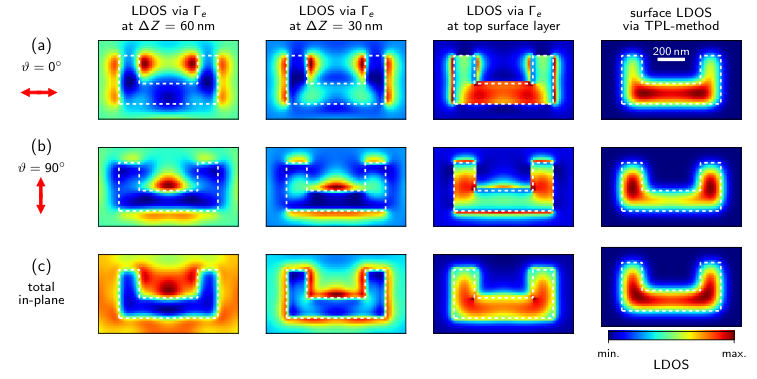
In figure 18 we show rasterscan simulations of the photonic LDOS above a U-shaped dielectric planar structure. The length is nm in the -direction, nm in the direction, its height is nm and the bar width is nm. Fig. 18a) shows the partial LDOS for -oriented dipole emitters, (b) the case of orientation and (c) the total LDOS in the structure plane. From left to right is shown the LDOS at decreasing distance to the structure (nm, nm and nm to the top surface). In the very right column the surface LDOS is calculated using the “TPL”-method (using a spotsize of nm, see also section 5.2). Comparing the LDOS at the top surface layer with the TPL-method, the general trends are reproduced. The differences are not very surprising, since the calculated quantities are not exactly the same. The TPL method gives a measure of the energy that can be coupled into the structure at the respective surface position using a focused beam. It is therefore only non-zero if the focused beam intersects with the structure. The LDOS corresponds to the efficiency of the radiative coupling between a dipolar emitter and the structure and is non-zero also outside the structure.

9 Evolutionary optimization of nanostructure geometries
9.1 Evolutionary optimization
A peculiarity of pyGDM is the EO module, provided together with the main pyGDM toolkit. The purpose of the EO module is to find nanostructure geometries that perform a certain optical functionality in the best possible way. This is also known as the “inverse problem” [58, 59]. We try to achieve this goal by formulating the optical property as an optimization problem which takes the geometry of the particle as input. Such problem will usually result in a complex, non-analytical function and hence cannot be solved by classical optimization methods like variants of the “Newton-Raphson method”.
In our approach we therefore optimize the problem using evolutionary optimization (EO) algorithms. The latter mimic natural selection to find ideal solutions to complex (often non-analytical) problems. The initial step is to define a “population” of random parameter-sets for the problem. These “individuals” are then evolved through a cycle of “reproduction” (mixing parameters between the individuals and application of random changes) and “selection” (problem evaluation and discarding weak solutions). After a sufficient number of iterations, hopefully an optimum parameter-set for the problem has been found. The evolutionary optimization cycle is depicted in figure 19a. Unfortunately, convergence can in principle never be guaranteed in EO. Convergence is therefore probably the most critical point in evolutionary optimization strategies. To ensure the credibility of the optimization results, a good stop-criterion and/or careful testing of the convergence and reproducibility of the solution for different initializations are crucial. For details on EO, we refer to the related literature, e.g. Ref. [60].
9.2 EO in pyGDM
pyGDM can be used to optimize particle geometries for nano-optical problems via evolutionary optimization. Our approach consists of three main ingredients:
- 1.
The structure-model: Constructs a particle geometry as function of a set of input-parameters which will be the free parameters for the optimization algorithm. It furthermore contains the simulation setup (via an instance of core.simulation). It is defined by a class inherited from
EO.models.BaseModel
(class)
- 2.
The problem: Defines the optimization target. This will usually be an optical property of the particle such as the scattering cross-section or its near-field enhancement. It is defined by a class inherited from
EO.problems.BaseProblem
(class)
- 3.
The EO algorithm: Finally the algorithm to solve the optimization problem
For (3.) we use the PyGMO / paGMO toolkit [61]. PyGMO not only offers a large spectrum of EO algorithms. It can furthermore distribute the population of solutions on several “islands” within the so-called “Generalized island model”. This allows for a very easy scaling of the evolutionary optimization on multi-processor architectures [62].
Note: In this context, the use of the generalized propagator in pyGDM is a clear asset. Optimization problems with the incident field shape and/or polarization as variable and a fixed structure geometry can be solved very efficiently. This includes problems like near-field shaping in adaptive optics [63].
9.3 Multi-objective optimization
pyGDM’s EO-module is also capable of treating multi-objective optimization problems, by internally addressing pyGMO’s according API. In other words, it is possible to search for nano-structure geometries optimizing multiple target properties simultaneously.
Such evolutionary multi-objective optimization (EMO) can in principle be done in two ways: The first approach consists in summarizing the multiple target values in one single fitness function, hence capturing the problem into a single objective optimization. In this case, the critical part is the construction of an appropriate fitness-value, which is usually not trivial at all. In the second approach, one searches for the set of “non-dominated” or “Pareto optimum” solutions, which is often called the “Pareto front”. It consists of solutions that are all optimal in the sense that an improvement in one of the target functions necessarily leads to a decrease in at least one of the other optimization targets. The obvious advantage is, that the individual objectives can be used as-is without the need to fiddle them into a single fitness-function. On the other hand, the latter approach additionally requires the selection of a single optimum solution from the set of Pareto optimum solutions. For a detailed introduction to EMO, see e.g. Ref. [64].
9.4 EO-Examples
We demonstrate the evolutionary optimization toolkit “EO” on some simple but illustrative problems.
9.4.1 Maximize scattering cross-section or scattering efficiency
For a first demonstration, we want to optimize the shape of a rectangular gold-antenna in order to obtain maximum scattering at a certain wavelength and for a fixed angle of the linear incident polarization. The free parameters are the length and width of the plasmonic rectangle (see Fig. 19b). The position of the rectangle (), the stepsize (nm) of the cubic mesh and the height of the antenna (nm) are fixed.
We run the EO of the rectangular shape with different optimization targets, the respective final best solutions are shown in figure 20: In (a) the scattering efficiency (i.e. the scattering cross-section divided by the geometrical cross-section ) is maximized for an incident plane wave with wavelength nm and linear polarization of along . In (b) maximum is searched for nm and . In (c) is again maximized for nm but a perpendicular polarization angle, hence . Finally, (d) shows and optimization of the scattering cross-section (instead of ), with otherwise equal configuration as in (c).
The first observation is, that the optimization is indeed capable of adjusting the size of the antenna such that the surface plasmon resonance occurs at the target wavelength. We also observe that while the optimization of the scattering efficiency ( given at the right of each plot) leads to thin rectangles with low geometric cross section, the optimization of the scattering cross section ( given at the left of each plot) leads to a structure of maximum allowed dimensions. This leads to a cross-section about twice as large as for the other antennas. The scattering efficiency on the other hand is significantly lower (about a factor ) compared to the optimizations shown in figure 20a-c.
9.4.2 Maximize electric field intensity
In a second example we want to find a structure to maximize the electric field intensity at a specific point , nm above the structure surface.
As structure to be optimized, we use again the rectangular gold-antenna of variable length and width with the same configuration as in the first example. Additionally we introduce as free parameters the offsets and , shifting the rectangle with respect to the origin of the coordinate system (see Fig. 19b). The structure is illuminated by a plane wave (nm), linearly polarized along .
We run the optimization for two different . The results are shown in figure 21. In both runs, the optimization found a plasmonic dipole antenna, resonant at the incident wavelength and shifted its position such that the hot-spot of maximum field enhancement lies at .
9.4.3 EMO: Double resonant plasmonic antenna
In a last example, we show how multiple objectives can be optimized concurrently in a single optimization, by calculating the Pareto-front. For the demonstration, we try to obtain structures that scatter light at two different wavelengths for perpendicular polarization angles of the incident plane wave. We choose a simple cross-like geometry model (structure placed in vacuum), consisting of the four free parameters and (see Fig. 19c).
The optimization goal is to simultaneously maximize for (1) a wavelength nm and an incident polarization along and (2) nm and an incident polarization along . The Pareto-front obtained by the evolutionary optimization is shown in figure 22. Scattering spectra of selected structures are shown in the top, their geometries are illustrated in the insets, labeled (1)-(3).
The optimization indeed found structures which maximize either one of the scattering-targets ((1) and (3)), or scatter light similarly strong for both target configurations (structure (2)). Note that the Pareto-front is not very smooth. In addition, the model seems not to be sufficiently sophisticated in order to obtain structures with equal for both target conditions. A more general structure model could probably provide better solutions for the problem.
Note:
10 Conclusion
In conclusion, we presented a python toolkit for electro-dynamical simulations in nano-optics, based on a volume discretization approach, the Green dyadic method. While other techniques like FEM may offer better accuracy, the main strength of pyGDM is the efficient treatment of large monochromatic problems with many illumination configurations, like raster-scan simulations. Such calculations can be solved very efficiently in pyGDM thanks to the concept of the generalized propagator. Furthermore, its simplicity is a great advantage of pyGDM. The high-level python API as well as many tools for rapid data analysis and visualization render standard nano-optical simulations very easy. Finally, the evolutionary optimization submodule is a unique feature, which allows to optimize nanostructure geometries for specific target optical properties. Scripts to reproduce all above shown examples, can be found online together with further, extensive documentation.
Acknowledgments
I gratefully thank Christian Girard and Arnaud Arbouet for their advise, help with the theory, careful proof-reading and for the fortran routines. I also want to thank Gérard Colas des Francs for helpful discussions and his contributions to the fortran code to which also Renaud Marty contributed. I finally thank Vincent Paillard and Aurélien Cuche for many inspiring discussions and proof-reading of the manuscript. This work was supported by Programme Investissements d’Avenir under the program ANR-11-IDEX-0002-02, reference ANR-10-LABX-0037-NEXT, and by the computing facility center CALMIP of the University of Toulouse under grant P12167.
Conflicts of interests
The author declares no competing financial interest.
11 Appendix – Accuracy, possible system size and limitations
Limitations
The limit for the number of discretization meshpoints depends mainly on the amount of RAM available in the machine. The memory requirement rises with (figure 6b). The computation time rises even proportional to (see also figure 6a), so at some point, the speed will be limiting as well. This effectively limits the number of meshpoints to .
Accuracy, large systems
To yield a reasonable accuracy, the discretization stepsize has to be sufficiently small (in the order of nm for plasmonics and dielectrics of refractive index ). For dielectrics with higher refractive index, the discretization should be further refined to yield accurate results. However, if the user is aware of the fact that the agreement will be only qualitative, approximative simulations are possible with larger discretization. In consequence, the memory requirement limits the applicability of pyGDM to the amount of material that can be simulated with good accuracy to (very rough estimation) nm3).
Small systems
When the size of the system is reduced, the discretization can be finer within the limit of the feasible -k meshpoints. Hence, the accuracy becomes better. One must only be aware, that pyGDM is a purely classical Maxwell solver. Therefore, the size of the system should not be reduced down to scales where quantum effects would occur (usually nm).
12 Appendix – Technical details
12.1 Reference system in pyGDM simulations
In pyGDM an asymptotic Green’s dyad is used which describes not only a substrate (“layer 1”, refractive index ), but also an additional cladding layer at a variable height above the substrate (“layer 3”, ). The nanoparticle is placed in the sandwich layer (“layer 2”, ), i.e. in-between layers 1 and 3. The distance between the substrate and the cladding layer can be specified by a spacing parameter. By default, , so if the index of the cladding layer “3” is not specified in the constructor of structures.struct, a reference system composed of a homogeneous environment above a dielectric substrate is assumed. To run a simulation without a substrate it is sufficient to simply set . The geometry of the pyGDM reference system is illustrated in figure 2.
The non-retarded Dyad used in pyGDM can be derived using the image charges method and gives good approximations for dielectric interfaces of low refractive index. A fully retarded Dyad for the 3-layer environment can also be calculated, which becomes necessary for instance at metallic interfaces [17, 68]. This might be implemented in future versions of pyGDM.
12.2 Structure geometry
The structure geometry in pyGDM is defined as a list of tuples, defining the positions of the meshpoints on either a cubic, or a hexagonal compact, regular grid.
pyGDM comes with some generators for common structures in nano-photonics. These geometries are available in the structures submodule. An overview of the available structures is shown in figure 23. Additional structures can easily be implemented at the example of the available generator functions. We suggest using the mesher-routines structures._meshCubic and structures._meshHexagonalCompact.
Additionally, planar structures can be generated from the brightness contrast of an image file, using
structures.image_to_struct
(function)
This may be used to create structures from a lithography-mask layout or also from scanning electron- or atomic force-microscopy images, to simulate “real” geometries from an experimental sample.
Finally, structure-geometries can be manipulated (rotated, “center of gravity” shifted to the origin) using
structures.rotate_XY
(function)
structures.center_struct
(function)
12.3 Material dispersion
pyGDM provides some basic dispersion models in its materials submodule:
materials.dummy generates a material object which returns a constant dielectric function. “silicon”, “gold” and “alu” provide the commonly used dispersion data for the respective materials.
However, usually one would use tabulated data for the dispersion. This can be done in pyGDM via
materials.fromFile
(class)
All dispersion containers “materials.class” provide an epsilon(wavelength) attribute, which is a function that returns the (complex) permittivity at wavelength (in nm).
By default, the tabulated data is interpolated linearly using numpy’s “interp”. Optionally, higher order spline interpolation is supported (based on scipy.interpolate.interp1d). Note that the latter may cause problems with python’s “pickling” technique, particularly in combination with the EO module.
12.4 Minimum working example script
12.5 Further tools available in pyGDM
12.5.1 Save and load simulations
To save and reload pyGDM simulations, the following functions are available. Saving and loading relies on python’s “pickle” technique:
tools.save_simulation
(function)
tools.load_simulation
(function)
12.5.2 Show information about simulations
To print detailed information about a pyGDM simulation, the following function can be used
tools.print_sim_info
(function)
alternatively, simply use “print sim_object”.
12.5.3 Generate coordinate list for D map
To calculate D data in pyGDM (e.g. near-field maps, c.f. figure 8d-g), we provide a tool to easily generate the D grid (in cartesian D space) for such data:
tools.generate_NF_map
(function)
12.5.4 Get index of specific field configuration
pyGDM uses keyword dictionaries to store multiple configurations of the incident field (such as several wavelengths, polarizations, focused beam positions). All possible permutations of the given keywords are stored in the core.simulation object and are attributed an index, by which they can unambiguously identified. In order to get the index of the field parameters that closest match specific search values (like a wavelength), one can use:
tools.get_closest_field_index
(function)
All field-configurations available in a simulation, sorted by their field-index, can be obtained by
tools.get_field_indices
(function)
12.5.5 Cubic stepsize from discretized structure
If the particle discretization is generated with another program then the pyGDM meshing functions (available in the structures submodule), it might be helpful to determine the stepsize of the structure. We provide a function, that computes the stepsize of a cubic mesh by calculating the closest distance between any two meshpoints (using scipy.spatial.distance.pdist).
tools.get_step_from_geometry
(function)
12.5.6 Get complex field as list of coordinate/field tuples
After running core.scatter, pyGDM stores the fields inside the particle in the core.simulation object as lists of the complex field components (). The () geometry coordinates are stored separately in the structures.struct object within the simulation description object. To generate complete field-lists of tuples , pyGDM provides the following functions:
tools.get_field_as_list
(function)
tools.get_field_as_list_by_fieldindex
(function)
Both return the complex field for a selected illumination configuration as list of coordinate / field tuples (), either from the raw field-object or from the simulation object and a field-index, respectively.
12.5.7 Generate D map from coordinate list
To map spatial data available as list of (coordinate-) tuples onto a plot-able 2D grid (e.g. for plotting a mapping with matplotlib.imshow), pyGDM provides
tools.map_to_grid_XY
(function)
12.5.8 Raster-scan field configurations
If a simulation with a large number of focused beam-positions has been performed, the available incident field configurations corresponding to full raster-scan maps can be obtained using
tools.get_possible_field_params_rasterscan
(function)
Analogously, the set of indices referring to the fields in the simulation.E which correspond to a particularly configured raster-scan, can be obtained via
tools.get_rasterscan_field_indices
(function)
Alternatively, the full set of fields inside the particle for a raster-scan with particular illumination-configuration can be obtained via
tools.get_rasterscan_fields
(function)
12.6 Dependencies
The core functionalities of pyGDM depend only on numpy. The compilation of the fortran parts require a fortran compiler such as gcc’s gfortran.
12.6.1 Dependencies: visu
All 2D visualization tools require matplotlib.
12.6.2 Dependencies: visu3D
All 3D visualization tools require mayavi.
12.6.3 Dependencies: tools
Several tools require scipy.
12.6.4 Dependencies: structures
Several structure-tools require scipy. image_to_struct requires PIL.
12.6.5 Dependencies: core.scatter: Solver (parameter “method”)
pyGDM includes wrappers to several scipy solvers but also other methods are supported. Below is given an exhaustive list of the available solvers and their dependencies. For benchmarks, see figure 6.
- 1.
“lu” (default) scipy.linalg.lu_factor (LU decomposition)
- 2.
“numpyinv” numpy.linalg.inv (if numpy is compiled with LAPACK: LAPACK’s “dgesv”, else a slower fallback routine)
- 3.
“dyson”: Own implementation, no requirements (sequence of Dyson’s equations [20])
- 4.
“scipyinv” scipy.linalg.inv (LAPACK’s “dgesv”)
- 5.
“pinv2”: scipy.linalg.pinv2 (singular value decomposition, SVD)
- 6.
“superlu”: scipy.sparse.linalg.splu (superLU [69])
- 7.
“cg”: scipy conjugate gradient iterative solver (scipy.sparse.linalg.bicgstab), by default preconditioned with scipy’s incomplete LU decomposition (superLU [69] via scipy.sparse.linalg.spilu)
- 8.
“pycg”: pyamg’s implementation of the bicgstab algorithm, optionally preconditioned with scipy’s incomplete LU decomposition. Recommended if multi-threading problems are encountered with scipy’s bicgstab implementation, which is not threadsafe
12.7 Compiling, installation
We provide a script for the easy compilation and installation via python’s “distutils” functionality. For this, simply run in the pyGDM root directory
python setup.py install
Alternatively, pyGDM can be compiled locally without installation via
python setup.py build
Or it may be installed to a user-defined location using the “--prefix=...” option.
Note:
The “setup.py” script requires numpy as well as a fortran compiler (tested with gfortran).
12.8 Possible future capabilities
The GDM can be used for manifold further calculations, which are to be included in future versions of pyGDM. A non-exhaustive list of possible future features includes
- 1.
2D structures (assuming infinite length along one coordinate)[70]
- 2.
- 3.
- 4.
- 5.
- 6.
materials with anisotropic susceptibility, e.g. birefringent media
- 7.
- 8.
quantum corrected model for plasmonic tunneling currents via junctions of inhomogeneous permittivity [77]
- 9.
- 10.
memory-efficient conjugate gradients solver including FFT-accelerated matrix-vector multiplications for large problems [27]
13 Appendix – Keyword arguments of the most important classes and functions
Most important classes
For a detailed explanation of the physical information contained by the below classes, see section 3.
core.simulation
(class)
constructor arguments:
1.
struct: instance of structures.struct
2.
efield: instance of fields.efield
structures.struct
(class)
constructor arguments:
1.
step: discretization stepsize (in nm)
2.
geometry: list of meshpoint coordinates (in nm)
3.
material: structure material dispersion, instance of materials.CLASS
4.
n1, n2: ref. index of substrate (n1) and environment (n2)
5.
normalization (optional): mesh-type dependent factor, default: “1” (cubic mesh)
6.
n3 (optional): ref. index of cladding
7.
spacing (optional): distance between substrate and cladding. default: “5000” (nm)
fields.efield
(class)
constructor arguments:
1.
field_generator: field generator function (e.g. from fields module)
2.
wavelengths: list of wavelengths at which to do the simulation (in nm)
3.
kwargs (optional): dict (or list of dict) with further kwargs for the field generator
Most important functions
pyGDM core
core.scatter / core.scatter_mpi
(function)
arguments:
1.
sim: instance of core.simulation
2.
method (optional): inversion method, default: “lu”
3.
multithreaded (optional): default: “True”
core.decay_rate
(function)
arguments:
1.
sim: instance of core.simulation
2.
method (optional): inversion method, default: “lu”
Post-processing
linear.extinct
(function)
arguments:
1.
sim: instance of core.simulation
2.
field_index: index of field-configuration
linear.nearfield
(function)
arguments:
1.
sim: instance of core.simulation
2.
field_index: index of field-configuration
3.
r_probe : list of coordinates at which to evaluate the near-field
Visualization
visu.structure
(function)
arguments:
1.
sim: instance of core.simulation
2.
projection (optional): default: “XY”
3.
color (optional): optional, matplotlib compatible color, default: “auto”
4.
scale (optional): scaling, default: “0.5”
visu.vectorfield
(function)
arguments:
1.
NF: list containing the complex field (list of 6-tuples . See also section 12.5.6: tools.get_field_as_list)
2.
projection (optional): default: “XY”
3.
slice_level (optional): using only fields at specific height. default: “none” superpose all vectors
visu.scalarfield
(function)
arguments:
1.
NF: list of 4-tuples containing the coordinates and scalar-field values ()
14 Appendix – GDM in the SI unit system
In order to facilitate the conversion between SI and cgs unit systems, in this section, we introduce the main GDM equations in SI units.
The Fourier transformed Maxwell equations are then:
| (48a) | ||||
| (48b) | ||||
| (48c) | ||||
| (48d) | ||||
From which the following wave equation can be derived:
| (49) |
This leads to the vectorial Lippmann-Schwinger equation in SI units (here for a vacuum reference system):
| (50) |
with the Green’s Dyad
| (51) |
where the definitions of , and given in equations (6)-(8) are still valid.
In Eq. (50) and its volume discretization
| (52) |
one has to use the susceptibility . For simplicity here we assumed a scalar .
Post-processing routines
Concerning the post-processing routines, some of the pre-factors need to be adapted. For instance, the factor before the sums of equations (39) and (40) writes in SI units:
| (53) |
with the refractive index .
The equations (43) and (44) for heat-generation, respectively the local temperature increase have to be multiplied by a factor .
Note:
In pyGDM the post-processing routines internally convert the results to SI compatible units. The “extinct” function for instance returns the cross sections in units of nm2, “heat” returns nano Watts and “temperature” returns ∘K. For the respective returned units, see the technical documentation of the routines in the online documentation of the API e.g. at https://wiechapeter.gitlab.io/pyGDM2-doc/apidoc.html.

15 Appendix – Conjugate gradients
The following applies to all pyGDM functions which solve the main GDM inversion problem. The conjugate gradients solver provides an alternative to full inversion of the coupled dipole problem which can – under circumstances – be preferable to complete matrix inversion.
- 1.
argument method: “cg” (requires scipy) or “pycg” (requires pyamg)
If we have a closer look at the matrix M (see Eq. (12)), we can make an interesting observation: While M is not exactly sparse, most of the entries have significantly smaller absolute values than very few large matrix elements. In Fig. 25 we show plots of the population of matrix for some selected nano-structures. These population plots work as illustrated in the following examples:
contains also phase-information and is therefore complex, hence we use the absolute values of the matrix elements for the population patterns. In addition, the maximum of the color-code in Fig. 25 is clipped to 10 % of the maximum absolute value in the matrix to increase the contrast. Clearly, the matrices contain very few entries with values of more than some % of the overall maximum and yet % of all elements are generally non-zero.
It turns out, that such matrices are good candidates for iterative solving using so-called “Krylow-subspace methods”. The most popular algorithm of this class is the conjugate gradients (CG) method and its derivations like biconjugate gradients (for non-symmetric problems) or complex CG [80]. A detailed description of the method can be found in Ref. [37] (chapter 2.7). The main idea of these iterative methods is, that the inverse of the matrix is in many cases not actually required. For simulations that massively make use of the generalized propagator (like raster-scan simulations), the CG technique is therefore not the method of choice. It may be on the other hand an advantageous approach, if we search a solution for that satisfies
| (54) |
for one single or only few incident field . During the CG-iterations, matrix-vector multiplications are performed following a minimization scheme in which converges eventually to . Theoretically, for a matrix CG converge to the exact solution after iterations and each iteration itself has a computational cost . In reality, the convergence is often very rapid in the beginning, and a solution with sufficient precision can be obtained after very few iterations, yielding a total computational cost instead of a scaling for exact inversion for example with LU-decomposition. Indeed, we find a -scaling for complete inversion by LU or Dyson’s sequence and a dependence when using conjugate gradients (Fig. 6a). Particularly for larger numbers of meshpoints, this allows a reduction of the simulation time, as shown in Fig. 6a.
15.1 Preconditioning
- 1.
argument pc_method: “ilu”, “lu” (both require scipy), “amg” (requires pyamg) or “none” (no preconditioning)
The speed of the convergence of conjugate gradients is crucially dependent on the condition of the matrix and generally can be massively improved by doing a preconditioning step before starting the actual iterative scheme. Let’s assume, of the equation system
| (55) |
would be the identity matrix . Then CG would have converged within the first iteration. A possible approach for preconditioning is therefore to reshape the problem using a matrix
| (56) |
If is a close approximation to , will be close to the identity and the system would converge very quickly under conjugate gradients iterations. Eq. (56) is called a right-preconditioned system. Consequently, a good preconditioner for our problem is a close approximation to the inverse of . Several algorithms exist to search pseudo-inverse matrices for preconditioning. A very popular one is the incomplete LU-decomposition (ILU) [81] that scales with and which is the default method in pyGDM.
15.2 Preconditioner recycling
- 1.
argument cg_recycle_pc: “True” (=default)
When calculating spectra using the GDM, the electric field in a particle is usually calculated for a large number of closely spaced wavelengths, at each of which the matrix is (incompletely) inverted. Most often, the electric field distribution changes only marginally for slightly different wavelengths and so does the matrix . Unfortunately, a very similar matrix is of little use for exact calculations, but we have seen in the preceding section that an approximation to the exact inverse can be a good preconditioner for CG.
When calculating dense spectra (i.e. many points on the wavelength axis), we can use this fact and significantly accelerate the calculation with conjugate gradients by recycling the preconditioner matrix until a certain lower limit for the speedup factor is reached. In other words, we will be using the same repeatedly for several consecutive wavelengths and only if the acceleration is below a speed-up limit, a new preconditioner is calculated and subsequently re-used for the following wavelengths. As shown in Fig. 26, this technique can divide the total calculation time easily by more than a factor .
Another possible application when preconditioner recycling may be beneficial is in series of simulations with many very similar or slowly transformed nano-structures like antennas of gradually increasing size.
Note:
The conjugate gradients solver is not very efficient for the moment and will be improved in future versions of pyGDM. In particular, in the specific case of the coupled dipole approximation it is possible to do very efficient vector/matrix multiplications by applying a fast Fourier transformation (FFT) scheme [27]. This is not yet implemented in pyGDM. The currently used third-party sparse-matrix solvers are not ideally suited regarding the dense matrix problem in pyGDM.
References
- [1] J. C. Maxwell, A Dynamical Theory of the Electromagnetic Field, Philosophical Transactions of the Royal Society of London 155 (1865) 459–512. doi:10.1098/rstl.1865.0008.
- [2] A. I. Kuznetsov, A. E. Miroshnichenko, M. L. Brongersma, Y. S. Kivshar, B. Luk’yanchuk, Optically resonant dielectric nanostructures, Science 354 (6314). doi:10.1126/science.aag2472.
- [3] P. Bharadwaj, B. Deutsch, L. Novotny, Optical Antennas, Advances in Optics and Photonics 1 (3) (2009) 438. doi:10.1364/AOP.1.000438.
- [4] S. Maier, Plasmonics: Fundamentals and Applications, Springer US, 2010.
- [5] C. Girard, O. J. F. Martin, A. Dereux, Molecular Lifetime Changes Induced by Nanometer Scale Optical Fields, Physical Review Letters 75 (17) (1995) 3098–3101. doi:10.1103/PhysRevLett.75.3098.
- [6] L.-J. Black, Y. Wang, C. H. de Groot, A. Arbouet, O. L. Muskens, Optimal Polarization Conversion in Coupled Dimer Plasmonic Nanoantennas for Metasurfaces, ACS Nano 8 (6) (2014) 6390–6399. doi:10.1021/nn501889s.
- [7] P. R. Wiecha, L.-J. Black, Y. Wang, V. Paillard, C. Girard, O. L. Muskens, A. Arbouet, Polarization conversion in plasmonic nanoantennas for metasurfaces using structural asymmetry and mode hybridization, Scientific Reports 7 (2017) 40906. doi:10.1038/srep40906.
- [8] A. Arbabi, Y. Horie, M. Bagheri, A. Faraon, Dielectric metasurfaces for complete control of phase and polarization with subwavelength spatial resolution and high transmission, Nature Nanotechnology 10 (11) (2015) 937–943. doi:10.1038/nnano.2015.186.
- [9] A. G. Curto, G. Volpe, T. H. Taminiau, M. P. Kreuzer, R. Quidant, N. F. van Hulst, Unidirectional Emission of a Quantum Dot Coupled to a Nanoantenna, Science 329 (5994) (2010) 930–933. doi:10.1126/science.1191922.
- [10] G. Baffou, R. Quidant, Thermo-plasmonics: Using metallic nanostructures as nano-sources of heat, Laser & Photonics Reviews 7 (2) (2013) 171–187. doi:10.1002/lpor.201200003.
- [11] M. Kauranen, A. V. Zayats, Nonlinear plasmonics, Nature Photonics 6 (11) (2012) 737–748. doi:10.1038/nphoton.2012.244.
- [12] J. Butet, P.-F. Brevet, O. J. F. Martin, Optical Second Harmonic Generation in Plasmonic Nanostructures: From Fundamental Principles to Advanced Applications, ACS Nano 13 (4) (2015) 10545–10562. doi:10.1021/acsnano.5b04373.
- [13] D. Griffiths, Introduction to Electrodynamics, Prentice-Hall International, 1989.
- [14] C. Girard, Near fields in nanostructures, Reports on Progress in Physics 68 (8) (2005) 1883–1933. doi:10.1088/0034-4885/68/8/R05.
- [15] G. S. Agarwal, Quantum electrodynamics in the presence of dielectrics and conductors. I. Electromagnetic-field response functions and black-body fluctuations in finite geometries, Physical Review A 11 (1) (1975) 230–242. doi:10.1103/PhysRevA.11.230.
- [16] C. Girard, E. Dujardin, G. Baffou, R. Quidant, Shaping and manipulation of light fields with bottom-up plasmonic structures, New Journal of Physics 10 (10) (2008) 105016. doi:10.1088/1367-2630/10/10/105016.
- [17] G. Colas des Francs, D. Molenda, U. C. Fischer, A. Naber, Enhanced light confinement in a triangular aperture: Experimental evidence and numerical calculations, Physical Review B 72 (16) (2005) 165111.
- [18] M. Paulus, P. Gay-Balmaz, O. J. F. Martin, Accurate and efficient computation of the Green’s tensor for stratified media, Physical Review E 62 (4) (2000) 5797–5807. doi:10.1103/PhysRevE.62.5797.
- [19] P. R. Wiecha, Linear and nonlinear optical properties of high refractive index dielectric nanostructures, PhD thesis, Université de Toulouse, Université Toulouse III - Paul Sabatier (Sep. 2016).
- [20] O. J. F. Martin, C. Girard, A. Dereux, Generalized Field Propagator for Electromagnetic Scattering and Light Confinement, Physical Review Letters 74 (4) (1995) 526–529. doi:10.1103/PhysRevLett.74.526.
- [21] A. Yaghjian, Electric dyadic Green’s functions in the source region, Proceedings of the IEEE 68 (2) (1980) 248–263. doi:10.1109/PROC.1980.11620.
- [22] C. Girard, A. Dereux, Near-field optics theories, Reports on Progress in Physics 59 (5) (1996) 657. doi:10.1088/0034-4885/59/5/002.
- [23] Y. Ould Agha, O. Demichel, C. Girard, A. Bouhelier, G. C. des Francs, Near-Field Properties of Plasmonic Nanostructures with High Aspect Ratio, Progress In Electromagnetics Research 146 (2014) 77–88. doi:10.2528/PIER14012904.
- [24] J. Kottmann, O. Martin, Accurate solution of the volume integral equation for high-permittivity scatterers, IEEE Transactions on Antennas and Propagation 48 (11) (2000) 1719–1726. doi:10.1109/8.900229.
- [25] A. Teulle, R. Marty, S. Viarbitskaya, A. Arbouet, E. Dujardin, C. Girard, G. Colas des Francs, Scanning optical microscopy modeling in nanoplasmonics, Journal of the Optical Society of America B 29 (9) (2012) 2431. doi:10.1364/JOSAB.29.002431.
- [26] B. T. Draine, P. J. Flatau, Discrete-dipole approximation for scattering calculations, Journal of the Optical Society of America A 11 (4) (1994) 1491. doi:10.1364/JOSAA.11.001491.
- [27] J. J. Goodman, B. T. Draine, P. J. Flatau, Application of fast-Fourier-transform techniques to the discrete-dipole approximation, Optics Letters 16 (15) (1991) 1198. doi:10.1364/OL.16.001198.
- [28] N. Geuquet, L. Henrard, EELS and optical response of a noble metal nanoparticle in the frame of a discrete dipole approximation, Ultramicroscopy 110 (8) (2010) 1075–1080. doi:10.1016/j.ultramic.2010.01.013.
- [29] F. J. García de Abajo, A. Howie, Retarded field calculation of electron energy loss in inhomogeneous dielectrics, Physical Review B 65 (11) (2002) 115418. doi:10.1103/PhysRevB.65.115418.
- [30] U. Hohenester, A. Trügler, MNPBEM – A Matlab toolbox for the simulation of plasmonic nanoparticles, Computer Physics Communications 183 (2) (2012) 370–381. doi:10.1016/j.cpc.2011.09.009.
- [31] J. Waxenegger, A. Trügler, U. Hohenester, Plasmonics simulations with the MNPBEM toolbox: Consideration of substrates and layer structures, Computer Physics Communications 193 (Supplement C) (2015) 138–150. doi:10.1016/j.cpc.2015.03.023.
- [32] U. S. Inan, R. A. Marshall, Numerical Electromagnetics: The FDTD Method, Cambridge University Press, 2011.
- [33] F. Baida, A. Belkhir, Finite difference time domain method for grating structures, in: Gratings: Theory and Numeric Applications, popov, e. Edition, Presses Universitaires de Provence, 2013, pp. 333–366.
- [34] Y. Cao, A. Manjavacas, N. Large, P. Nordlander, Electron Energy-Loss Spectroscopy Calculation in Finite-Difference Time-Domain Package, ACS Photonics 2 (3) (2015) 369–375. doi:10.1021/ph500408e.
- [35] J. Hoffmann, C. Hafner, P. Leidenberger, J. Hesselbarth, S. Burger, Comparison of electromagnetic field solvers for the 3D analysis of plasmonic nanoantennas, Vol. 7390, International Society for Optics and Photonics, 2009, p. 73900J. doi:10.1117/12.828036.
- [36] A. F. Oskooi, D. Roundy, M. Ibanescu, P. Bermel, J. D. Joannopoulos, S. G. Johnson, MEEP: A flexible free-software package for electromagnetic simulations by the FDTD method, Computer Physics Communications 181 (2010) 687–702. doi:doi:10.1016/j.cpc.2009.11.008.
- [37] W. Press, Numerical Recipes 3rd Edition: The Art of Scientific Computing, Cambridge University Press, 2007.
- [38] J. Smajic, C. Hafner, L. Raguin, K. Tavzarashvili, M. Mishrikey, Comparison of Numerical Methods for the Analysis of Plasmonic Structures, Journal of Computational and Theoretical Nanoscience 6 (3) (2009) 763–774. doi:10.1166/jctn.2009.1107.
- [39] M. A. Yurkin, A. G. Hoekstra, The discrete dipole approximation: An overview and recent developments, Journal of Quantitative Spectroscopy and Radiative Transfer 106 (1) (2007) 558–589. doi:10.1016/j.jqsrt.2007.01.034.
- [40] S. Viarbitskaya, A. Teulle, R. Marty, J. Sharma, C. Girard, A. Arbouet, E. Dujardin, Tailoring and imaging the plasmonic local density of states in crystalline nanoprisms, Nature Materials 12 (5) (2013) 426–432. doi:10.1038/nmat3581.
- [41] R. W. Boyd, Intuitive explanation of the phase anomaly of focused light beams, Journal of the Optical Society of America 70 (7) (1980) 877. doi:10.1364/JOSA.70.000877.
- [42] L. Novotny, B. Hecht, Principles of Nano-Optics, Cambridge University Press, Cambridge ; New York, 2006.
- [43] P. R. Wiecha, A. Arbouet, A. Cuche, V. Paillard, C. Girard, Decay rate of magnetic dipoles near nonmagnetic nanostructures, Physical Review B 97 (8) (2018) 085411. doi:10.1103/PhysRevB.97.085411.
- [44] G. Colas des Francs, Optique sub-longueur d’onde et fluorescence moléculaire perturbée, PhD thesis, Université Paul Sabatier Toulouse, CEMES-CNRS (2002).
- [45] R. Carminati, A. Cazé, D. Cao, F. Peragut, V. Krachmalnicoff, R. Pierrat, Y. De Wilde, Electromagnetic density of states in complex plasmonic systems, Surface Science Reports 70 (1) (2015) 1–41. doi:10.1016/j.surfrep.2014.11.001.
- [46] P. A. Huidobro, X. Shen, J. Cuerda, E. Moreno, L. Martin-Moreno, F. J. Garcia-Vidal, T. J. Cui, J. B. Pendry, Magnetic Localized Surface Plasmons, Physical Review X 4 (2) (2014) 021003. doi:10.1103/PhysRevX.4.021003.
- [47] P. R. Wiecha, C. Majorel, C. Girard, A. Arbouet, B. Masenelli, O. Boisron, A. Lecestre, G. Larrieu, V. Paillard, A. Cuche, Simultaneous mapping of the electric and magnetic photonic local density of states above dielectric nanostructures using rare-earth doped films, arXiv:1801.09690arXiv:1801.09690.
- [48] E. Lassalle, A. Devilez, N. Bonod, T. Durt, B. Stout, Lamb shift multipolar analysis, JOSA B 34 (7) (2017) 1348–1355. doi:10.1364/JOSAB.34.001348.
- [49] C. Girard, J.-C. Weeber, A. Dereux, O. J. F. Martin, J.-P. Goudonnet, Optical magnetic near-field intensities around nanometer-scale surface structures, Physical Review B 55 (24) (1997) 16487–16497. doi:10.1103/PhysRevB.55.16487.
- [50] B. T. Draine, The Discrete-Dipole Approximation and its Application to Interstellar Graphite Grains, Astrophysical Journal 333 (1988) 848–872.
- [51] L. Novotny, Allowed and forbidden light in near-field optics. II. Interacting dipolar particles, Journal of the Optical Society of America A 14 (1) (1997) 105–113. doi:10.1364/JOSAA.14.000105.
- [52] G. Baffou, R. Quidant, C. Girard, Heat generation in plasmonic nanostructures: Influence of morphology, Applied Physics Letters 94 (15) (2009) 153109. doi:10.1063/1.3116645.
- [53] G. Baffou, R. Quidant, C. Girard, Thermoplasmonics modeling: A Green’s function approach, Physical Review B 82 (16) (2010) 165424. doi:10.1103/PhysRevB.82.165424.
- [54] P. R. Wiecha, M.-M. Mennemanteuil, D. Khlopin, J. Martin, A. Arbouet, D. Gérard, A. Bouhelier, J. Plain, A. Cuche, Local field enhancement and thermoplasmonics in multimodal aluminum structures, Physical Review B 96 (3) (2017) 035440. doi:10.1103/PhysRevB.96.035440.
- [55] S. Viarbitskaya, A. Cuche, A. Teulle, J. Sharma, C. Girard, A. Arbouet, E. Dujardin, Plasmonic Hot Printing in Gold Nanoprisms, ACS Photonics 2 (6) (2015) 744–751. doi:10.1021/acsphotonics.5b00100.
- [56] Y. H. Fu, A. I. Kuznetsov, A. E. Miroshnichenko, Y. F. Yu, B. Luk’yanchuk, Directional visible light scattering by silicon nanoparticles, Nature Communications 4 (2013) 1527. doi:10.1038/ncomms2538.
- [57] I. M. Hancu, A. G. Curto, M. Castro-López, M. Kuttge, N. F. van Hulst, Multipolar Interference for Directed Light Emission, Nano Letters 14 (1) (2014) 166–171. doi:10.1021/nl403681g.
- [58] D. Macias, A. Vial, D. Barchiesi, Application of evolution strategies for the solution of an inverse problem in near-field optics, JOSA A 21 (8) (2004) 1465–1471. doi:10.1364/JOSAA.21.001465.
- [59] T. W. Odom, E.-A. You, C. M. Sweeney, Multiscale Plasmonic Nanoparticles and the Inverse Problem, The Journal of Physical Chemistry Letters 3 (18) (2012) 2611–2616. doi:10.1021/jz300886z.
- [60] H.-P. P. Schwefel, Evolution and Optimum Seeking: The Sixth Generation, John Wiley & Sons, Inc., New York, NY, USA, 1993.
- [61] F. Biscani, D. Izzo, C. H. Yam, A Global Optimisation Toolbox for Massively Parallel Engineering Optimisation, arXiv:1004.3824 [cs, math]arXiv:1004.3824.
- [62] D. Izzo, M. Ruciński, F. Biscani, The Generalized Island Model, in: F. F. de Vega, J. I. H. Pérez, J. Lanchares (Eds.), Parallel Architectures and Bioinspired Algorithms, no. 415 in Studies in Computational Intelligence, Springer Berlin Heidelberg, 2012, pp. 151–169.
- [63] T. Brixner, F. J. García de Abajo, J. Schneider, C. Spindler, W. Pfeiffer, Ultrafast adaptive optical near-field control, Physical Review B 73 (12) (2006) 125437. doi:10.1103/PhysRevB.73.125437.
- [64] K. Deb, Multi-Objective Optimization Using Evolutionary Algorithms, Vol. 16, Wiley, 2001.
- [65] P. R. Wiecha, A. Arbouet, C. Girard, A. Lecestre, G. Larrieu, V. Paillard, Evolutionary multi-objective optimization of colour pixels based on dielectric nanoantennas, Nature Nanotechnology 12 (2) (2017) 163–169. doi:10.1038/nnano.2016.224.
- [66] C. Girard, P. R. Wiecha, A. Cuche, E. Dujardin, Designing Thermoplasmonic Properties of Metallic Metasurfaces, Journal of Optics (just accepted). arXiv:1804.01111, doi:10.1088/2040-8986/aac934.
- [67] P. R. Wiecha, A. Arbouet, C. Girard, A. Lecestre, G. Larrieu, V. Paillard, Multi-resonant silicon nanoantennas by evolutionary multi-objective optimization, in: Computational Optics II, Vol. 10694, International Society for Optics and Photonics, 2018, p. 1069402. doi:10.1117/12.2315123.
- [68] R. Marty, C. Girard, A. Arbouet, G. Colas des Francs, Near-field coupling of a point-like dipolar source with a thin metallic film: Implication for STM plasmon excitations, Chemical Physics Letters 532 (Supplement C) (2012) 100–105. doi:10.1016/j.cplett.2012.02.058.
- [69] X. S. Li, An Overview of SuperLU: Algorithms, Implementation, and User Interface, ACM Transactions on Mathematical Software 31 (3) (2005) 302–325. doi:10.1145/1089014.1089017.
- [70] M. Paulus, O. J. F. Martin, Green’s tensor technique for scattering in two-dimensional stratified media, Physical Review E 63 (6) (2001) 066615. doi:10.1103/PhysRevE.63.066615.
- [71] P. R. Wiecha, A. Arbouet, C. Girard, T. Baron, V. Paillard, Origin of second-harmonic generation from individual silicon nanowires, Physical Review B 93 (12) (2016) 125421. doi:10.1103/PhysRevB.93.125421.
- [72] A. Arbouet, A. Mlayah, C. Girard, G. Colas des Francs, Electron energy losses and cathodoluminescence from complex plasmonic nanostructures: Spectra, maps and radiation patterns from a generalized field propagator, New Journal of Physics 16 (11) (2014) 113012. doi:10.1088/1367-2630/16/11/113012.
- [73] C. Girard, A. Dereux, O. J. F. Martin, M. Devel, Generation of optical standing waves around mesoscopic surface structures: Scattering and light confinement, Physical Review B 52 (4) (1995) 2889–2898. doi:10.1103/PhysRevB.52.2889.
- [74] A. Kwadrin, A. F. Koenderink, Probing the electrodynamic local density of states with magnetoelectric point scatterers, Physical Review B 87 (12) (2013) 125123. doi:10.1103/PhysRevB.87.125123.
- [75] B. Gallinet, O. J. F. Martin, Electromagnetic Scattering of Finite and Infinite 3D Lattices in Polarizable Backgrounds, Theoretical And Computational Nanophotonics (Tacona-Photonics 2009) 1176 (2009) 63–65.
- [76] P. C. Chaumet, A. Sentenac, Simulation of light scattering by multilayer cross-gratings with the coupled dipole method, Journal of Quantitative Spectroscopy and Radiative Transfer 110 (6–7) (2009) 409–414. doi:10.1016/j.jqsrt.2008.12.004.
- [77] R. Esteban, A. G. Borisov, P. Nordlander, J. Aizpurua, Bridging quantum and classical plasmonics with a quantum-corrected model, Nature Communications 3 (2012) 825. doi:10.1038/ncomms1806.
- [78] J.-J. Greffet, R. Carminati, Image formation in near-field optics, Progress in Surface Science 56 (3) (1997) 133–237. doi:10.1016/S0079-6816(98)00004-5.
- [79] J. A. Porto, R. Carminati, J.-J. Greffet, Theory of electromagnetic field imaging and spectroscopy in scanning near-field optical microscopy, Journal of Applied Physics 88 (8) (2000) 4845–4850. doi:10.1063/1.1311811.
- [80] P. Joly, G. Meurant, Complex conjugate gradient methods, Numerical Algorithms 4 (3) (1993) 379–406. doi:10.1007/BF02145754.
- [81] X. S. Li, M. Shao, A Supernodal Approach to Incomplete LU Factorization with Partial Pivoting, ACM Transactions Mathematical Software 37 (4) (2011) 43. doi:10.1145/1916461.1916467.