Radiation resistant LGAD design
Abstract
In this paper, we report on the radiation resistance of 50-micron thick Low Gain Avalanche Diodes (LGAD) manufactured at the Fondazione Bruno Kessler (FBK) employing different dopings in the gain layer. LGADs with a gain layer made of Boron, Boron low-diffusion, Gallium, Carbonated Boron and Carbonated Gallium have been designed and successfully produced at FBK. These sensors have been exposed to neutron fluences up to and to proton fluences up to to test their radiation resistance. The experimental results show that Gallium-doped LGAD are more heavily affected by the initial acceptor removal mechanism than those doped with Boron, while the addition of Carbon reduces this effect both for Gallium and Boron doping. The Boron low-diffusion gain layer shows a higher radiation resistance than that of standard Boron implant, indicating a dependence of the initial acceptor removal mechanism upon the implant density.
Keywords:
Silicon , Timing , LGAD , Acceptor RemovalThe LGAD design evolves the standard silicon sensors design by incorporating low, controlled gain [1] in the signal formation mechanism. The overarching idea is to manufacture silicon detectors with signals large enough to assure excellent timing performance while maintaining almost unchanged levels of noise [2].
Charge multiplication in silicon sensors happens when the charge carriers (electrons and holes) are in electric fields of the order of kV/cm [3]. Under this condition, the electrons (and to less extent the holes) acquire sufficient kinetic energy to generate additional e/h pairs by impact ionization. Field values of 300 kV/cm can be obtained by implanting an appropriate acceptor (or donor) charge density (of the order ) that, when depleted, locally generates very high fields. For this reason, an additional doping layer has been added at the junction in the LGAD design, Figure 1.

1 Initial acceptor removal in LGAD sensors
It has been shown in previous studies [4, 5] that neutrons and charged hadrons irradiations reduce the value of gain in LGADs. This effect is due to the initial acceptor removal mechanism that progressively deactivates the acceptors forming the gain layer. The effects of initial acceptor removal on the silicon sensor bulk has been first measured in standard Boron-doped silicon sensors more than 20 years ago [6]. Concurrently with the initial acceptor removal mechanism, irradiation causes also the creation of acceptor-like defects due to the creation of deep traps. The combined effects are described by equation (1) [2, 7]
| (1) |
where = 0.02 [cm-1] (see for example chapter 5 of [8]), the irradiation fluence [ cm-2], the initial (after a fluence ) acceptor density [cm-3], and [cm2] is a constant that depends on the initial acceptor concentration and on the type of irradiation. The first term of equation (1) accounts for acceptor creation by deep traps while the second term for the initial acceptor removal mechanism. The factor can be rewritten as , making more apparent its meaning: is the fluence needed to reduce the initial doping density to 1/e of its initial value.
The microscopic origin of the acceptor removal mechanism has not been fully understood, however, it is plausible that the progressive inactivation of the Boron atoms with irradiation happens via the formation of ion-acceptor complexes. In this model, the active (substitutionals) doping elements are removed from their lattice sites due to a 2-step process: (i) the radiation produces interstitial Si atoms that subsequently (ii) inactivate the doping elements via kick-out reactions (Watkins mechanism [9]) that produce ion-acceptor complexes (interstitials) [10].
Secondary Ion Mass Spectrometer (SIMS) measurements support this view: Figure 2 shows the densities of Boron atoms forming the gain layer as a function of depth in a new (M83) and a heavily irradiated (M80, irradiated to ) LGAD where the gain layer has completely disappeared. The SIMS were performed in the central area of 1 mm2 LGADs. Remarkably, the SIMS results are almost identical: the decrease of the active gain layer doping in irradiated sensors does not correspond to a disappearance of the Boron atoms, only to their inactivation. The SIMS were performed in the central area of 1 mm2 LGADs

1.1 A parametrization of the acceptor removal mechanism
In a simple model of acceptor removal, the number of initial acceptor atoms deactivated by radiation is given by the product of the fluence times the silicon atomic density times the cross section for an impinging particle to deactivate an acceptor :
| (2) | |||||
| (3) |
where . Following the two-step model outlined above, the expression of can be written as the product of the cross section between radiation and Silicon () times the number of interstitials generated in the scattering () times the probability of capturing an acceptor ():
| (4) |
Note that the presence of impurities (Carbon, Oxigen,…) influence the value of as they might intercept the interstitial atoms before they reach the acceptors.
Equation (2) assumes that each interstitial atom created by radiation is in the proximity of acceptors, however this might not be the case at low acceptor density. For this reason, a proximity function needs to be included in equation (2): this function describes the probability that an interstitial atom is in the vicinity of an acceptor atom. The analytic form of is not unique, any smooth function that goes to 0 at low acceptor density and to 1 at large density is acceptable, for example:
| (5) |
where is a fit parameter indicating the acceptor density at which an interstitial state has a probability of 0.5 of being in the vicinity of an acceptor and is an exponent that needs to be determined experimentally. Figure 3 shows the values of D1, D2 and D3 ( = 1, 2 or 3) with .

Combining equations (2) and (5), the expression linking the fluence to the number of deactivated acceptors is:
| (6) | |||||
| (7) |
where and are fit parameters. Analytic expressions of using a linear (D1), a surface (D2) and a volumetric (D3) proximity function were tried, finding the best agreement between models and data with = 2, mb , and . The result indicates that the clusters have a cylindrical shape since spherical shape would have yield to . Using these numbers, the parameterizations of equation (6) without the proximity function and with each of the three functions (D1, D2, and D3) are superposed in Figure 4 to experimental points. The experimental points of B - neutrons (Boron gain layer irradiated with reactor neutrons) are taken from [11, 12, 13], the B - protons (Boron gain layer irradiated with 800 MeV/c protons) from [11, 13] while Ga - neutrons (Gallium gain layer irradiated with reactor neutrons) from [14, 15].
The effect of the proximity function is important at low initial acceptor density, where the overlap probability between interstitial states and acceptors is small and therefore a higher fluence is needed to have initial acceptor removal. It is important to stress that the acceptor removal rate might differ upon the irradiation type (pions, protons, neutrons), the irradiation energy, and the acceptor element (Boron or Gallium), however, for lack of statistics, Figure 4 shows a single common fit.
The inverse of the density provides a rough indication of the average volume of each cluster of defects created by a particle: yields to a cluster size of Å, which is compatible with the current estimates [16, 17].

Using the D2 parametrization, the absolute and relative effect of radiation on the initial acceptor density can be studied. The left plot of Figure 5 reports the number of removed acceptors per incident particle as a function of : it varies from 1 at to 60 at . Even though the number of removed acceptors increases with , the fraction of removed acceptor is strongly decreasing as a function of (Figure 5, right plot) demonstrating that high initial acceptor densities are less affected by radiation.
From the asymptotic behavior of the left plot of Figure 5 we can measure the product , and combining this value with the value of mb , we can calculate :
| (8) | |||||
| (9) |
Both numbers are consistent with the results shown in [17] for 1 MeV neutron on Silicon: 4 mb and .

Finally, using the terms described above, the expression of the coefficient can be written as:
| (10) |
where the capture coefficient depends upon the doping used for the gain layer and the presence of additional impurities such as Carbon or Oxygen.
Acceptor creation and initial acceptor removal mechanisms described by equation (1) happen concurrently in the multiplication layer as well as in the bulk. The evolutions of several initial doping densities as a function of neutron fluence are shown schematically in Figure 6: the initial Boron doping is removed as the fluence increases and in the meantime new acceptor-like states are created. At sufficiently high values of fluence, all initial doping values converge on the doping density of the high resistivity PiN diodes, indicating a complete disappearance of the initial acceptor density.

2 Production of LGAD with different gain layer doping
Three hypotheses have been put forward for the design of more radiation hard LGADs: (i) it has been reported in [15, 18] that Gallium might be less prone than Boron to the Watkins mechanism, (ii) the presence of Carbon atoms might slow down the acceptor removal mechanism by producing ion-carbon complexes instead of ion-acceptor complexes, and (iii) a narrower doping layer with higher initial doping should be less prone to the acceptor removal mechanism than a wider doping layer with a lower initial doping.
To test these hypotheses, 50-micron thick LGAD sensors with 5 different gain layer configurations have been manufactured at the Fondazione Bruno Kessler 11 1 FBK, Fondazione Bruno Kessler, Trento, Italy : (i) Boron (B), (ii) Boron low-diffusion (B LD), (iii) Gallium (Ga), (iv) carbonated Boron (B+C), and (v) carbonated Gallium (Ga+C). This production is called UFSD2. It is important to note that carbon enrichment has been done uniquely in the volume of the gain layer to avoid a sharp increase of the leakage current. Details on the production have been presented in [19], a short summary of the UFSD2 production is shown in Table 1: 18 6-inch wafers were processed, 10 with a B-doped and 8 with a Ga-doped gain layer. The B-doped gain layer wafers W3-10 have 3 splits dose, in 2% steps, while the Ga-doped gain layer wafers W11-19 have also 3 splits of dose, however in 4% steps. Two splits of B-doped and one of the Ga-doped gain layers have been co-implanted with Carbon, with two different doses of Carbon. Two wafers with a B-doped gain layer (W1,2) were exposed to a reduced thermal load during production to minimize the diffusion of Boron (Boron low-diffusion). The Ga-doped wafers, given the higher diffusivity of Gallium, were also exposed to a reduced thermal load, however, the width of the resulting Gallium implant is nevertheless wider even than that of the B-doped gain layer with a high thermal load.
| Wafer | Dopant | Gain Dose | Carbon | Diffusion | irradiation |
|---|---|---|---|---|---|
| 1 | Boron | 0.98 | Low | n | |
| 2 | Boron | 1.00 | Low | ||
| 3 | Boron | 1.00 | High | p | |
| 4 | Boron | 1.00 | Low | High | |
| 5 | Boron | 1.00 | High | High | |
| 6 | Boron | 1.02 | Low | High | p, n |
| 7 | Boron | 1.02 | High | High | |
| 8 | Boron | 1.02 | High | n | |
| 9 | Boron | 1.02 | High | ||
| 10 | Boron | 1.04 | High | ||
| 11 | Gallium | 1.00 | Low | ||
| 12 | Gallium | 1.00 | Low | ||
| 13 | Gallium | 1.04 | Low | ||
| 14 | Gallium | 1.04 | Low | p, n | |
| 15 | Gallium | 1.04 | Low | Low | p, n |
| 16 | Gallium | 1.04 | High | Low | |
| 18 | Gallium | 1.08 | Low | ||
| 19 | Gallium | 1.08 | Low |
UFSD2 layout comprises of many hundreds of devices, from single diodes to large arrays of pads and strips [19]. For this irradiation campaign, pairs of PiN - LGAD diodes were used, as shown in Figure 7. Combined PiN-LGAD irradiation is a very useful tool in assessing the evolution of the LGAD behavior with fluence, as at each irradiation step the PiN diodes are used as a reference.

2.1 Properties of LGAD with different gain layer doping
Figure 8 shows on the top pane representative 1/C2-V curves for B and B+C doped gain layers LGADs while on the bottom those of Ga and Ga+C doped gain layers. The voltage necessary to deplete the gain layer, , is proportional to the average active doping in the gain layer:
| (11) |
where is the thickness of the gain layer, normally , and the electron electric charge. Assuming a constant value of , is directly proportional to . In the 1/-V curves, can be recognized as the point where the 1/C2-V curve starts a sharp increase, while the voltage of the diode full depletion, , is where the 1/C2 becomes constant. The voltage difference between and , , is proportional to the doping of the sensor bulk. For non irradiated sensors, as those shown in Figure 8, is of the order of a few volts indicating a doping of atoms/cm3. We indicate measured with the 1/-V curves with the symbol .

It is visible in the plot that Carbon implantation reduces the activated fraction of Gallium, while the Carbon effects on Boron is minimal: is on average 0.3V smaller for B+C LGADs with respect to that of B LGADs. A discussion of the effects of Carbon co-implantation can be found in [20].
The measurements were taken with the Keysight B1505A parameter analyzer using as the model of the silicon detector a circuit. The 1/C2-V curves were obtained at room temperature with a probing frequency of 1 kHz. The value of the frequency was varied between 1 and 3 kHz finding no dependence of the results on the operating frequency. Analyzing how changes with bias, we noticed that in coincidence with the curve presents a sharp decrease, allowing for an easy identification of the exact voltage of the gain layer depletion. We indicate measured with the -V curves with the symbol . The correspondence between and is shown in Figure 9 for a sensor from W1 irradiated to 3.
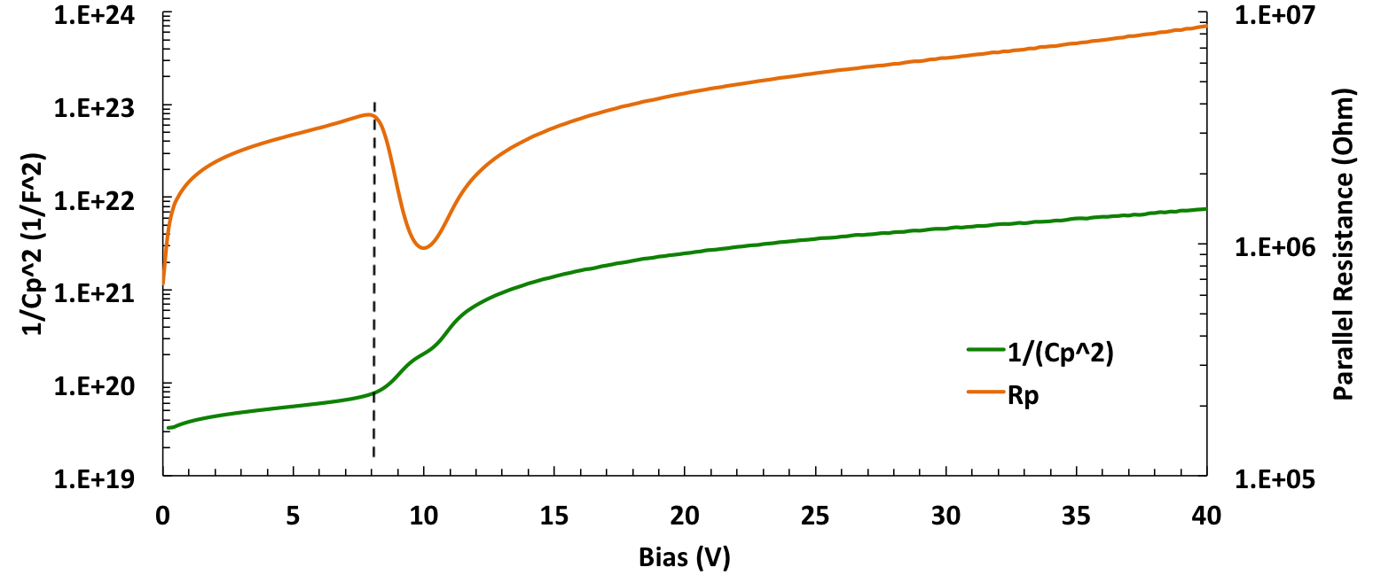
In the following analysis, the gain layer depletion voltage has been determined using a combination of the and values: at low fluences both and are easily identifiable, while for fluences above 1 the position of is easier to identify. The combination of and allows determining with an uncertainty of 0.5 V.
An interesting parameter to understand the acceptor removal mechanism is the spatial extension of the gain layer. Table 2 reports, in arbitrary unit, the measured FWHM of the gain layer implants for the wafers exposed to irradiation. The implant widths have been extracted from the doping profiles obtained from the 1/C2-V curves using the relationship:
| (12) |
where is the doping density at a depth and is the diode’s area.
| Wafer | Dopant | Gain Dose | Width [a.u.] |
|---|---|---|---|
| 1 | B LD | 0.98 | 1 |
| 3 | B | 1.00 | 1.3 |
| 6 | B + C | 1.02 | 1.3 |
| 8 | B | 1.02 | 1.3 |
| 14 | Ga | 1.04 | 2.0 |
| 15 | Ga + C | 1.04 | 1.7 |
These widths are consistent with the observation reported in [20] that carbon co-implantation might yield to narrower implant widths.
3 Irradiation campaign
Table 3 reports the wafers and the irradiation steps used in the irradiation campaign. A set of LGADs was irradiated without bias with neutrons in the JSI research reactor of TRIGA type in Ljubljana. The neutron spectrum and flux are well known [21] and the fluence is quoted in 1 MeV equivalent neutrons per (). A different set of LGADs was irradiated with protons at the IRRAD CERN irradiation facility [22]. The IRRAD proton facility is located on the T8 beam-line at the CERN PS East Hall where the primary proton beam with a momentum of 24 GeV/c is extracted from the PS ring. In IRRAD, irradiation experiments are performed using the primary protons, prior reaching the beam dump located downstream of the T8 beam line. After irradiation, the devices were annealed for 80 min at 60 oC. Afterward, the devices were kept in cold storage at -20 oC. The table reports the actual number of protons: the fluences in can be obtained by multiplying the proton fluences by the NIEL factor (NIEL = 0.6).
| Wafer | Dopant | Gain Dose | n fluence [] | p fluence [] |
|---|---|---|---|---|
| 1 | B LD | 0.98 | 0.2, 0.4, 0.8, 1.5, 3.0, 6.0 | |
| 3 | B | 1.00 | 0.2, 0.9, 3.9 | |
| 6 | B + C | 1.02 | 0.2, 0.4, 0.8, 1.5, 3.0, 6.0 | 0.9, 3.9 |
| 8 | B | 1.02 | 0.2, 0.4, 0.8, 1.5, 3.0, 6.0 | |
| 14 | Ga | 1.04 | 0.2, 0.4, 0.8, 1.5, 3.0, 6.0 | 0.9, 3.9 |
| 15 | Ga + C | 1.04 | 0.2, 0.4, 0.8, 1.5, 3.0, 6.0 | 0.9, 3.9 |
4 Simulation of different initial acceptor removal rate
As reported in equation (1), the initial acceptor removal effect is parametrized by the function . Using the simulation program WF222 2 Shareware at http://cern.ch/nicolo [23], the effect of larger or smaller values of on the reduction of the gain has been simulated. Figure 10 reports the bias voltage needed to keep a constant gain value = 10 as a function of neutron fluence for the situation where the value of is twice, a half or a quarter of the presently measured value of . The simulation has been calculated using the parametrization shown in equation (1), with = 0.02 and the values (in unit of []) shown in the legend. On the plot, the measured points from Hamamatsu LGADs are also reported [5].

As Figure 10 shows, when the gain layer doping is progressively deactivated by irradiation, the bias voltage should be increased to compensate for the reduction of the electric field generated by the gain layer. Smaller values of move the need to increase the bias voltage to progressively higher fluences, making LGAD operation more stable.
5 Results
Figure 11 shows the evolution of the foot position () with increasing neutrons irradiation. The lowest irradiation level is , and the fluence increases by a factor of 2 in each of the following curves.
These plots show clearly that the decrease of as a function of irradiation for carbonated gain layers is smaller than that of non-carbonated gain layers: for equal fluence, carbonated gain layers retain a higher active doping. Comparing the 4 plots in Figure 11, it is evident that the slopes of the 1/C2 curves at equal fluence are similar, indicating, via equation (12), that the doping of the bulk is evolving in the same way for all sensors.
The coefficient can be measured by fitting an exponential function to the fraction of still active gain layer as a function of fluence, as shown in equation (13):
| (13) |
The fractions of active gain layer as a function of fluence are shown in Figure 12 for neutron irradiation and in Figure 13 for proton irradiation, together with the exponential fits.


Table 4 reports the compilation of measured values of for neutron () and proton () irradiation, and their ratios, ordered in decreasing value. The value of each coefficient has been estimated averaging the measurements of 2 irradiated samples. From the spread of the two measurements, and the uncertainty of the fit, an error of has been assigned to the determination of while, given the presence of only one measurement per fluence, the error on has been evaluated to be .
| Gain Layer | |||||
|---|---|---|---|---|---|
| No NIEL | No NIEL | NIEL | NIEL | ||
| Ga | 7.1 | 9. | 0.79 | 15. | 0.47 |
| B | 5.4 | 6.5 | 0.83 | 10.8 | 0.50 |
| B LD | 4.7 | ||||
| Ga + C | 4.0 | 4.2 | 0.95 | 7.0 | 0.57 |
| B + C | 2.1 | 3.3 | 0.63 | 5.5 | 0.38 |
For clarity, Table 5 reports the value of the fluence for neutrons and protons. Since the coefficient represents the flux needed to remove of the initial acceptor, Table 5 shows that a carbonated gain layer can withstand more than twice the radiation of a non-carbonated gain layer.
| Gain Layer | ||
|---|---|---|
| neutrons irrad. | protons irrad. | |
| Ga | 0.14 0.02 | 0.11 0.02 |
| B | 0.18 0.03 | 0.15 0.04 |
| B LD | 0.21 0.05 | |
| Ga + C | 0.25 0.06 | 0.24 0.09 |
| B + C | 0.48 0.23 | 0.30 0.14 |
6 Analysis
Several results can be extracted from Table 4 :
- •
The addition of Carbon improves the radiation resistance: the coefficients are about a factor of two smaller for B+C and Ga+C LGADs with respect of those of B or Ga. Since no other condition besides the addition of Carbon was changed, we can determine that the presence of Carbon reduces the value of the coefficient .
- •
Considering the real value of proton fluences, the measured and coefficients are compatible with each other, albeit the values are consistently higher. This effect indicates that the cross section to remove an acceptor, , is similar for a 1 MeV neutron and a 24 GeV proton.
- •
If the NIEL factor is applied to the protons fluence (NIEL = 0.6 for 24 GeV/c protons), the factors are almost twice .
- •
Narrower and more doped gain layer implants are less prone to initial acceptor removal: B LD has a lower coefficient than B. This is consistent with the expectation from the right pane of Figure 5 that shows that the relative importance of acceptor removal decreases with increasing initial doping density .
- •
The measured coefficients for Gallium doping are larger than those for Boron doping. This difference is partly due to the lower Gallium density used in W14 with respect of the Boron density in W3 and W8, however, the difference is larger than what it would be just due to this effect. This fact might indicate a higher acceptor removal rate of Gallium doping with respect of that of Boron doping. In [15], a lower acceptor removal rate of Gallium has been measured with respect of the data reported in this work, however, the reason might be that the initial Gallium density in [15] was higher than that of this work.
The gain in LGADs is required to be 20 - 30: this fact determines that the total amount of doping in the gain layer is roughly a constant in every LGAD. This given amount of doping can be distributed over narrower or wider implants, varying the doping density: equation (6) predicts that in LGADs with wider and less doped implants the initial acceptor removal mechanism is faster. The values of the coefficients as a function of the implant widths reported in Table 2 are shown in Figure 14: the plot clearly shows that in wider implants the initial acceptor removal mechanism is faster. This effect holds true also for carbonated gain layers.

A compilation of values of for neutron irradiation measured in this work and in [11, 12, 13, 14, 15] is shown in Figure 15. All sensors are 50-micron thick, however, they differ slightly in the doping profile as they don’t all have the same gain. The plot reports measurements for LGADs manufactured by CNM with a Gallium or a Boron gain layer, 4 different types of Boron LGADs manufactured by HPK (indicated with the names 50A, 50B, 50C and 50D in order of increasing gain layer doping levels) and several LGADs manufactured by FBK. The carbonated gain layers have clearly the largest values of , followed by B LD: the 1/e fluence for B+C LGADs is almost .
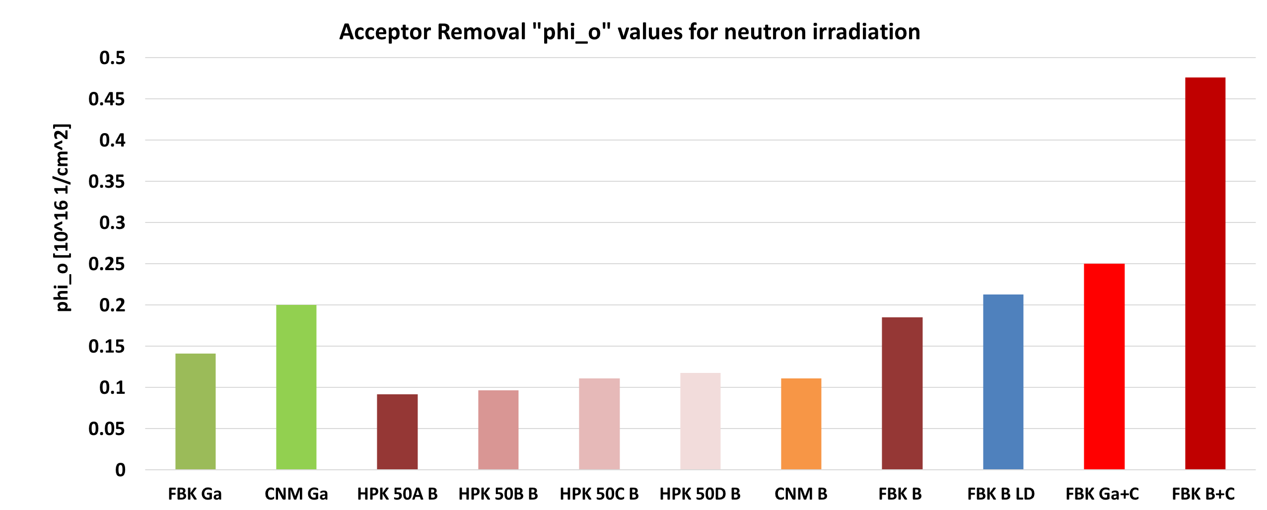
Figure 16 updates Figure 4 including the results obtained in this analysis: the new points cluster around . The value of has been obtained by computing the gain layer doping profile using the relationship, shown in equation (12), between the derivative of the curve and the doping at a depth .

7 Measurement of the gain due to the gain-layer after a fluence of and .
Using a collimated picosecond laser system with a light spot diameter of 20 microns and a wavelength of 1064 nm, the gains of B, B LD, B+C, Ga and Ga+C LGADs were measured as a function of bias voltage for 3 neutron irradiation levels: and . The value of the gain was obtained as the ratio of the signal areas obtained in an LGAD and in a PiN diode irradiated to the same fluence.
The results are shown in Figure 17: the top left plot shows the gain curves before irradiation, while the following 5 plots show the gain normalized to the respective unirradiated gain at Bias = 150V. As expected, B+C is the most radiation resistant LGAD: after a fluence of the gain layer still generate at bias = 500V the same gain as it had when not irradiated at bias = 150V. Likewise, Ga is the weakest retaining at 500V only 10% of the initial gain.

Confirming the results on the values of the coefficient, carbonated gain layers (B+C and Ga+C) show higher gain values than those without Carbon for the same fluence level. Likewise, B LD maintains higher gain values than B; at only B+C gain layer is still active. It is possible that by optimizing the Carbon dose this effect can be further enhanced.
8 Conclusions and outlook
50-micron thick LGADs manufactured by FBK with 5 different types of gain layer doping (B, B+C, Ga, Ga+C and B LD) have been irradiated with neutrons and protons. The results show that (i) carbonated gain layer are at least a factor of two more radiation resistant than the equivalent non-carbonated gain layer, (ii) Gallium doping is less radiation resistant than Boron doping, (iii) narrower gain layer implants are more radiation resistant than wider implants, (iv) considering the true fluence value, protons with 24 GeV/c momentum are similarly harmful than 1 MeV neutrons with respect of the initial acceptor removal mechanism, and that (v) if the fluence of protons with 24 GeV/c momentum is converted using the NIEL factor to 1 MeV equivalent neutrons, proton irradiation is much more harmful than that from 1 MeV neutrons .
Carbonated gain layer holds the possibility of designing silicon sensors with gain with enhanced radiation resistance. We plan to further investigate the property of carbonated gain layer by producing gain layers with several carbon doses, to optimize the radiation resistance of the LGAD design. We are confident that these findings, albeit obtained for LGAD sensors, can be successfully implemented in other silicon sensors with gain such as SiPM and APD.
9 Acknowledgments
We acknowledge the fundamental contributions coming from the discussions, and active collaboration of the RD50 colleagues. We recognize the key contributions of the irradiation facilities at Ljubjiana and IRRAD at CERN. Part of this work has been financed by the European Union’s Horizon 2020 Research and Innovation funding program, under Grant Agreement no. 654168 (AIDA-2020) and Grant Agreement no. 669529 (ERC UFSD669529), and by the Italian Ministero degli Affari Esteri and INFN Gruppo V
References
References
- [1] G. Pellegrini, et al., Technology developments and first measurements of Low Gain Avalanche Detectors (LGAD) for high energy physics applications, Nuclear Instruments and Methods in Physics Research A 765 (2014) 12–16.
- [2]
H. F.-W. Sadrozinski, A. Seiden, N. Cartiglia,
4D tracking with
ultra-fast silicon detectors, Reports on Progress in Physics 81 (2) (2018)
026101.
URL http://stacks.iop.org/0034-4885/81/i=2/a=026101 - [3] W. Maes, K. De Meyer, R. Van Overstraeten, Impact ionization in silicon: A review and update, Solid-State Electronics 33 (1999) 705–718.
- [4] G.Kramberger, et al., Radiation effects in Low Gain Avalanche Detectors after hadron irradiations, Journal of Instrumentation 10 (2015) P07006.
- [5] Z. Galloway, et al., Properties of HPK UFSD after neutron irradiation up to 6E15 n/cm2, (2017) arXiv:1707.04961.
- [6]
S. Terada, et al.,
Proton
irradiation on p-bulk silicon strip detectors using 12 GeV PS at
KEK, Nuclear Instruments and Methods in Physics Research Section A 383 (1)
(1996) 159 – 165.
doi:10.1016/S0168-9002(96)00748-6.
URL http://www.sciencedirect.com/science/article/pii/S0168900296007486 - [7]
M. Mandurrino, et al.,
Numerical
simulation of charge multiplication in ultra-fast silicon detectors (ufsd)
and comparison with experimental data, NSS/MIC IEEE Atlanta, 2017, submitted
to IEEE Nuclear Transaction.
URL https://www.eventclass.org/contxt_ieee2017/download/media?hash=$2y$13$BYBKhVqHCribI5uxmX.JfufYlrAIVzhDJGSQOexR1eteDVyfn8yMK - [8]
J. Balbuena, et al., RD50 Status
Report 2008 - Radiation hard semiconductor devices for very high
luminosity colliders (CERN-LHCC-2010-012. LHCC-SR-003).
URL http://cds.cern.ch/record/1291631 - [9]
B. Henderson, Defects and
Their Structure in Nonmetallic Solids, Nato Science Series B:, Springer US,
2013.
URL https://books.google.it/books?id=w3_rBwAAQBAJ - [10]
R. Wunstorf, et al.,
Investigations
of donor and acceptor removal and long term annealing in silicon with
different boron/phosphorus ratios, Nuclear Instruments and Methods in
Physics Research Section A 377 (2) (1996) 228 – 233, proceedings of the
Seventh European Symposium on Semiconductor.
doi:10.1016/0168-9002(96)00217-3.
URL http://www.sciencedirect.com/science/article/pii/0168900296002173 - [11]
G. Kramberger, et al.,
Radiation effects in
low gain avalanche detectors after hadron irradiations, Journal of
Instrumentation 10 (07) (2015) P07006.
URL http://stacks.iop.org/1748-0221/10/i=07/a=P07006 - [12]
G. Kramberger, et al.,
Radiation
hardness of thin low gain avalanche detectors, Nuclear Instruments and
Methods in Physics Research Section A 891 (2018) 68 – 77.
URL http://www.sciencedirect.com/science/article/pii/S0168900218301682 - [13] G. Kramberger, et al. Overview of sensor radiation tolerance at HL-LHC levels [online] (HSTD11, 2017).
- [14] M. del Mar Carulla Areste, et al. Last measurements and developments on LGAD detectors [online] (TREDI2017, 2017).
- [15]
G. Kramberger, et al.,
Radiation
hardness of gallium doped low gain avalanche detectors, Nuclear Instruments
and Methods in Physics Research Section A: Accelerators, Spectrometers,
Detectors and Associated Equipment 898 (2018) 53 – 59.
doi:https://doi.org/10.1016/j.nima.2018.04.060.
URL http://www.sciencedirect.com/science/article/pii/S0168900218305771 - [16] S. Meroli. Radiation Damage in Silicon Detector [online].
- [17]
M. Huhtinen,
Simulation
of non-ionising energy loss and defect formation in silicon, Nuclear
Instruments and Methods in Physics Research Section A 491 (1) (2002) 194 –
215.
doi:https://doi.org/10.1016/S0168-9002(02)01227-5.
URL http://www.sciencedirect.com/science/article/pii/S0168900202012275 - [18]
A. Khan, et al.,
Strategies
for improving radiation tolerance of Si space solar cells, Solar Energy
Materials and Solar Cells 75 (1) (2003) 271 – 276, pVSEC 12 Part II.
doi:10.1016/S0927-0248(02)00169-1.
URL http://www.sciencedirect.com/science/article/pii/S0927024802001691 - [19]
G. Paternoster,
New
developments in Ultra Fast Silicon Detectors at FBK, 31th RD50
Workshop, CERN, Geneva, 2017.
URL https://indico.cern.ch/event/663851/contributions/2787294/attachments/1562040/2484362/RD50_17_11_ext.pdf - [20]
Y. Shimizu, et al.,
Impact of carbon
co-implantation on boron distribution and activation in silicon studied by
atom probe tomography and spreading resistance measurements, Japanese
Journal of Applied Physics 55 (2) (2016) 026501.
URL http://stacks.iop.org/1347-4065/55/i=2/a=026501 - [21] L. Snoj, G. Zerovnik, A. Trkov, Computational analysis of irradiation facilities at the JSI TRIGA reactor, Applied Radiation and Isotopes 70 (2012) 483–488.
- [22] B. Gkotse, et al. Irradiation Facilities at CERN [online].
- [23] F. Cenna, et al., Weightfield2: A fast simulator for silicon and diamond solid state detector, Nuclear Instruments and Methods in Physics Research Section A 796 (2015) 149 – 153, proceedings of the 10th International Conference on Radiation Effects on Semiconductor Materials Detectors and Devices. doi:10.1016/j.nima.2015.04.015.