Characterizing Complementary Bipolar Junction Transistors by Early Modelling, Image Analysis, and Pattern Recognition
Abstract
This work reports an approach to study complementary pairs of bipolar junction transistors, often used in push-pull circuits typically found at the output stages of operational amplifiers. After the data is acquired and pre-processed, an Early modeling approach is applied to estimate the two respective parameters (the Early voltage and the proportionality parameter ). A voting procedure, inspired on the Hough transform image analysis method, is adopted to improve the identification of . Analytical relationships are derived between the traditional parameters current gain () and output resistance () and the two Early parameters. It is shown that tends to increase with for fixed , while depends only on , varying linearly with this parameter. Several interesting results are obtained with respect to 7 pairs of complementary BJTs, each represented by 10 samples. First, we have that the considered BJTs occupy a restricted band along the Early parameter space, and also that the NPN and PNP groups are mostly segregated into two respective regions in this space. In addition, PNP devices tended to present an intrinsically larger parameter variation. The NPN group tended to have higher magnitude and smaller than PNP devices. NPN transistors yielded comparable and larger than PNP transistors. A pattern recognition method was employed to obtain a linear separatrix between the NPN and PNP groups in the Early space and the respective average parameters were used to estimate respective prototype devices. Two complementary pairs of the real-world BJTs with large and small parameters differences were used in three configurations of push pull circuits, and the respective total harmonic distortions were measured and discussed, indicating a definite influence of parameter matching on the results.
Keywords:
Complementary pair, bipolar junction transistors, Early effect, characterization, linearity, push pull, LDA, Hough transform voting, THD, characteristic surface, current gain, output resistance, LDA, supervised classification, parameter variability.“Unity and complementarity constitute reality.”
W. Heisenberg
I Introduction
Transistors, in their discrete or integrated versions, remain at the heart of modern electronics. While these devices typically operate as switches in digital electronics, they are often used as amplifiers in linear or analog electronics. As implied by its own name, linear electronics usually requires these amplifiers to be as much linear as possible, in order to avoid distortions and preserve the original signal information, except for the changes in amplitude magnification that constitutes the main purpose of amplification (e.g. [16, 5, 24, 23, 27]). As it could be expected, the success in achieving good linearity of transistors depends, to a large extent, on characterizing their electronic properties, as well as modeling these devices, which can then be combined into circuits with improved linearity and other functionalities (e.g. filtering, mixing, etc.).
The beginnings of modern electronics can be traced back to the transistor invention [22]. Bipolar junction transistors – BJTs – followed suit, playing a decisive role in the popularization of electronic equipments. BJTs, still largely used nowadays, are current-controlled devices typically characterized by their current gain and output resistance . One of the problems that initially challenged the applications of BJTs is the fact that tends to vary largely among samples even from the very same lot. Other important properties of a BJT, such as its output resistance , are also subjected to variability. Ultimately, it was the systematic application of negative feedback (e.g. [2]) that paved the way to the widespread application of BJTs in electronics. The principle here is to exchange gain for parameter invariance, linearity and extended bandwidth (e.g. [2, 19, 3]), though it should be reminded that these effects are respective to each of the four types of electronic feedback (e.g. [2, 19, 3]). However, despite its impressive efficacy, there are limits to what can be accomplished with negative feedback. For instance, strong nonlinearities will require more intense negative feedback levels and respectively implied large gain reductions.
One of the simplest amplifying approaches using BJTs is the common emitter circuit operating in classes A (e.g. [5, 18]), in which the operation point is often located near the center of the linear region excursion (assuming symmetric signals) in order to optimize linearity and signal excursion. Unfortunately, this circuit requires substantial constant DC biasing, implying in heating and energy loss. An alternative approach, using a complementary pair of transistors – one PNP and one NPN, is the push-pull configuration (e.g. [24, 23, 27, 14, 16, 5]), operating in B or AB classes. Basically, in the former case, the positive part of the input signal is amplified by the NPN transistor, while the negative feeds the PNP BJT, therefore allowing null biasing and virtually no loss of DC power, also reducing thermal dissipation. The push-pull configuration is particularly important in electronics as it is adopted as output stage for many off-the-shelf operational amplifiers (OpAmps) [21, 26].
Yet, all these circuit types are not completely linear. First, we have the fact that and vary with the input signal magnitude, implying nonlinearities. Shortcomings also arise in the simplest push-pull configuration: (i) it is prone to thermal runaway, so that special care is required to limit the output current, (ii) it incorporates an inherent nonlinearity occurring as the signal of input signal crosses-over the null operation point, and (iii) two power supplies are now required (one positive and another negative). Though negative feedback (e.g. [2, 19, 3]) is typically employed in order to minimize this unwanted distortion, a recent study [10], considering a set of individual NPN BJTs operating in Class A, has suggested that moderate levels of negative feedback may not be enough to guarantee total BJT parameters invariance. Therefore, proper negative feedback action may benefit from starting with a good linearity level.
Though a better understanding of the operation of BJT as building blocks can contribute to devising better circuit configurations, BJTs turn out to be relatively complicated to characterize as a consequence of quantum mechanics effects, variability of fabrication parameters, contamination, among other issues. One of the most interesting manners to better understand a BJT (as well as any other transistor) is by using some modeling approach. A particularly simple, geometrical model based on the Early effect [11] was recently proposed that allows an intuitive representation of the transistor transfer curve (or function) by using only two parameters: the Early voltage () as well as the proportionality parameter (it has been experimentally verified in [11] and in this work that, usually, ). While traditional parameters such as and output resistance vary with the collector voltage () and current (), the two Early model parameters, and remain mostly constant (inside the linear operation region) for a given BJT. Thus, in a sense the Early parameterization seems to be more intrinsic and natural to BJTs.
The main purpose of the present work is to address the questions of modeling and characterization of the properties of complementary small signal transistors. Starting with experimental data corresponding to the voltages and currents of complementary pairs of BJTs subjected to DC scanning, we then applied the Early approach so as to map each device into the Early space, defined by the respective Early voltage () and the proportionality parameter . However, unlike in [11], estimation is herein performed by using a voting scheme inspired on the image analysis technique known as the Hough transform (e.g. [15, 9, 7]). By reducing the interference between the isoline projections into the axis, while emphasizing the coherent isolines, this methodology has potential for improving the accuracy for and estimation. Analytical relationships are also established between the Early parameters and and the more traditional current gain and output resistance parameters of BJTs. It is found that the average values of , namely tend to increase with for fixes . It is also verified that the output resistance increases linearly with the magnitude of and is completely independent of . In principle, however, the relationship between and was unknown, but the reported experimental results demonstrated that they tend to vary so as to keep within a relatively narrow range. These results also corroborated the linear relationship between and , namely ( is the base current) for all considered devices, as had been suggested in a previous work [11]. The estimation errors for and were found to be relatively small, being somewhat larger for the PNP cases than the NPN as a consequence of the larger parameter variation of the former group. The distributions of , , , and the amount of votes obtained for each isoline in the space were estimated and showed several interesting features. Two other parameters, corresponding to the regression offset while estimating the isolines as well as the relationship between and were also discussed in terms of the respective densities. The pairwise relationship between and resulted in two well-separated groups corresponding to the NPN and PNP transistors in both the Early and the spaces. Several additional interesting results were obtained, including the larger parameter variation of PNP devices and other differentiating properties. A pattern recognition method, namely linear discriminant analysis (LDA), was then applied in order to identify an optimal linear separation boundary between the two types of transistores, and the respective average parameters were used to estimate prototypical configurations for the NPN and PNP devices. An analytical development considering the derived equations with respect to total harmonic distortion in simplified common emitter configurations showed that the THD for the considered circumstances does not vary with , being a function of only. In order to illustrate the application potential of the reported methods and results, three pairs with varying parameter similarity were used to build three push pull circuit configurations, and the results confirm the importance of parameter matching for reducing the THD level.
This article starts by briefly presenting the three considered push pull configurations using complementary pairs of BJT, and proceeds by describing the data acquisition system, the experimental procedure, and pre-processing. The Early effect, voltage and modeling is then presented, together with equations for relating the Early parameters locally with the more traditional parameters and . However, these expressions can only characterize these relationships locally, for specific settings. They are here extended to express relationships between and and averages of and estimated through the whole operating region in the space, allowing a direct bridge between these two alternative parametric representations. The enhanced method for Early parameter estimation, based on Hough transform voting, is then described, illustrated, and discussed. The obtained results are reported and discussed next, first by individual densities, then in pairwise fashion between parameters. The definition of a prototypical Early space and NPN/PNP groups is also presented. Two complementary pairs with varying levels of parameter similarity are then employed in three push pull circuit configurations and the respective THDs are measured and discussed. This article concludes by recapitulating its main contributions and relating several prospects for future investigations.
II Three Push-Pull Configurations
Figure 1 depicts the simplest push-pull circuit including a complementary pair of transistors (PNP and NPN), marked as and . The input signal enters the bases of these two transistors, which have their collector-base junctions inversely biased and the base-emitter junctions directly biased. The positive portion of the input signal is amplified at , and the negative part is dealt with by . The outputs of these two transistors are linearly superimposed onto the resistive load (), adding up the positive and negative parts of the amplification. In a sense, the two complementary transistors act in integrated fashion, almost as a single device. Two power supplies are required, typically and . Observe that cross-over noise is implied by the offset voltages (about ) induced by the forward biased base-emitter junctions. It is interesting to notice that the push-pull configuration can be thought of as a combination of two complementary common emitter circuits biased at null voltage, but with the difference that the output sign is inverted as a consequence of deriving it from the emitters rather than the collectors. Observe that the currents entering the collectors have not other option (except for effects such as current leakage) than leaving the transistor and flowing through the load resistance. As in single transistor common emitter configurations, negative feedback (e.g. [2, 19, 3]) will tend to increase the output resistance, which is not desirable when driving reactive loads because it can lead to phase distortion.
Several means can be applied to minimize the unwanted cross-over distortion. Two possible approaches are shown in Figures 2, and Fig. 2. In the first case, two diodes are added so as to compensate the offset (about ) implied by the forward bias of the base-collector junctions. The resistors are added in order to bias the diodes. The circuit in Figure 2 includes an operational amplifier (op amp) for implementing negative feedback. Now, the input signal is driven into the positive lead of the op and, while the negative monitors the output signal at the load resistance .
III The Data Acquisition System
Each of the considered transistors was scanned by a custom-designed microprocessed system, yielding respective voltages and currents. The basic experimental set-up is shown in Figure 4, with respect to measurements of NPN and PNP devices, respectively. Recall that, in these two circuit configurations, all voltages and currents in the PNP are opposite to those in the NPN case. For simplicity’s sake all voltages and currents in the PNP case, which are all negative, are used in the present article in magnitude (positive values)..
DAC-generated voltages are applied at the points and , and the voltages at these points, as well as at the points and , are acquired by respective ADCs. The base and collector currents can be immediately determined from these voltage values, taking into account Ohm’s law and the values of and . The data is obtained by scanning from to at steps and, for each of the values, is scanned from to at steps. The herein reported experiments considered 256 points of resolution for and 128 points for . Thus, the characteristic surface of each transistor can be obtained by sliding the load line with a load resistance , as a consequence of the variable . Other scanning procedures can be used, leading to similar results as the characteristic surface of a transistor does not depend on external compontens. Observe that the value of is not critical and nearly the same characteristic surfaces, which depends only on the device and not on the attached resistances, will be obtained for the same BJT by using different values of , the absolute maximum ratings being observed.
The acquisition system uses a 16-bit microprocessor connected to a host providing mass memory resources (SD card) and internet connection The microprocessor subsystem also includes RAM and ROM memory as well as decoding and buffering circuitry. The microprocessed system is illustrated in Figure 5. A 12-bit twin digital-analog converter (DAC) is used, with respective driving buffers allowing programmable gain and offset. The signal acquisition is performed by a 12-bit quadruple multiplexed input analog-digital converter (ADC), and each channel is provided with separate buffering and sample/hold circuitry. Observe that all sample-and-hold circuits are strobed simultaneously to guarantee a snapshot of the DC voltage state of the monitored circuit, improving the coherence of the measured values. The digital and analog portions of this system occupy separate printed circuit boards for improved noise immunity, with the analog board being cased in a special shielding box. All power supply inputs and voltage rails are thoroughly decoupled. The observed noise level at the experiment portion of the analog board is in the order of the smallest division of the ADCs. The microprocessed subsystem connects to a host computer in order to allow internet access and mass memory (mainly SD card), and the data is analyzed in another, separated off-the-shelf microcomputer.
IV Acquisition and Pre-Processing
The four acquired voltages, , , , and , as well as the derived currents and , are then used in order to obtain the isolines of the transistor characteristic surface, which are illustrated in Figure 19 . This is done as follows: First, the data indices are properly reorganized in order to derived the isolines obtained respectively to each represented as functions of . Next, each isoline is slightly smoothed with an average filter along , in order to reduce eventual acquisition and resolution noise. Then, a linear resampling (actually an undersampling) is applied along these isolines (the interpolation free variable corresponds to ) so as to obtain a fixed, angularly equispaced, number of isolines for every transistor and reinforce the quality of the signals. As a consequence the step isolines from one isoline to the next is not the same for all transistors, but the is covered in a more uniform manner. We have adopted for all reported experiments.
V The Early Modeling Approach
Discovered by James M. Early in 1952 ([13]), the Early effect corresponds to an important phenomenon taking place inside junction transistors. Basically, the width of space charge at the base decreases as collector voltage is increased, yielding an increase of the current gain . This phenomenon is dominant in defining the collector conductance and is used in several BJT modes jointly with several other parameters. Graphically, the Early effect can be simple and neatly identified by a convergence of the isolines at a negative value (the Early voltage) along axis, as illustrated in Figure 6, which also shows the involved variables and the rectangular region of interest (delimited by the axes and the dashed lines) in which our analysis is based. This region is characterized by forward biasing of the base-emitter junction and inverse bias of the collector-base junction. It is argued here that, to a good extent, the electronic properties of a junction transistor (e.g. and ) in the linear region(disregarding the relatively small strips for the cut-off and saturation regions) are to a large extent determined by . For instance, the larger the magnitude value of this voltage, the larger the output resistance . At the same time, larger the magnitude of may also affect , but this depends on how the angle varies with . Henceforth, is given in radians values. A relationship between and the values of average through the region is derived further in this article. Observe that the Early parameterization can be understood as being more intrinsic, natural and effective than the more traditionally used approaches, because the Early parameters and mostly do not vary with or in the linear region. Yet, it is possible to derive other more traditional parameters from the Early formulation, as done in this work.
A simple model of junction transistors by using only the Early effect has been reported recently, [11] which is henceforth adopted. This model, which is restricted to the linear region of operation, involves only two parameters: (i) and (ii) , the latter corresponding to the constant of proportionality between and θ (i.e. ). This linear relationship, which is henceforth adopted in this work, was observed for several real-world BJTs [11] and confirmed for the BJT devices adopte in the present work. Given only these two parameters, and the defining a isoline, , indexed by , can be easy and conveniently obtained as:
| (1) | |||
Observe that acts as a conductance, having (Mho, or Siemens) as unit.
Alternatively, we have that:
| (2) | |||
The value of for which the isolines cross the axis at its maximum value can be immediately calculated as:
| (3) |
which implies .
The main traditional parameters of the junction transistor — namely the current gain , the output resistance , as well as the transresistance — can now be determined as:
| (4) | |||
| (5) | |||
| (6) |
The simplicity and graphical intuition of these equations are a welcomed consequence of the straightforward Early modeling approach.
Table 1 shows the theoretically obtained isolines for several combinations of values of the parameters and . Observe that these parameters are given for the whole first coordinate system quadrant, ignoring the saturation and cut-off region for simplicity’s sake. In real-world transistors, these two regions would limit, to a relatively small extent, the region of linear operation of the junction transistor respectively. These case-examples illustrate the behavior of the Early model parameters and with respect to isolines equispaced by in the space for 9 combinations of values of the and parameters. If is kept constant (as well as the bounding region of the space), BJTs with larger magnitude will have larger . However, it does not necessarily follow that junction transistors with larger will have larger or smaller average . The inference of this dependency is part of the objectives of the current work. Actually, because the average current gain in small signal industrialized transistors tend to be roughly similar, it could be expected that devices having larger magnitude will tend to have smaller (or vice-versa), in order to keep the current gain nearly constant among devices. The relationship between these parameters will be further explored in the experimental sections of this article.
![[Uncaptioned image]](1801.06025v2/plot_-20_3.jpeg) |
![[Uncaptioned image]](1801.06025v2/plot_-20_4.jpeg) |
![[Uncaptioned image]](1801.06025v2/plot_-20_5.jpeg) |
![[Uncaptioned image]](1801.06025v2/plot_-60_3.jpeg) |
![[Uncaptioned image]](1801.06025v2/plot_-60_4.jpeg) |
![[Uncaptioned image]](1801.06025v2/plot_-60_5.jpeg) |
![[Uncaptioned image]](1801.06025v2/plot_-100_3.jpeg) |
![[Uncaptioned image]](1801.06025v2/plot_-100_4.jpeg) |
![[Uncaptioned image]](1801.06025v2/plot_-100_5.jpeg) |
Because BJTs have been traditionally characterized by the and parameters, it is interesting to derive relationships between these parameters and and . One of the disadvantages of the more traditional approach is that and vary along the characteristic space. Indeed, both these parameters will continuously change as the transistor voltages and currents vary during normal operation. So, we need to consider the average values of these two parameters within a given region (operation space), which are henceforth expressed as and . Other regions, or even curves (e.g. load lines), of interest can be taken into account while deriving these averages. These relationships, derived analytically by integrating the two parameters along the operation region , are given as follows:
| (7) | |||
| (8) |
where is the area of the region through which the parameters are integrated. In the present case, it corresponds to the area of the operation region , so that .
It follows from these relationships that varies in a non-linear way with and linearly with . The output resistance, however, does not vary with . Figure 7 depicts the values of in terms of and , for and , respectively. A peak average current gain exceeding 2000 is observed, corresponding to the parameter configuration . Because typical small signal BJTs are known to have average current gain nearly between 50 and 500, only a relatively small region of the space will be populated by real-world devices, which is indeed confirmed in the experimental part of this work.

The linear relationship between and is presented in Figure 8. It follows that increased output resistances will be obtained for large magnitude values of .

VI Numerical Estimation of Early Model Parameters
So far we have discussed the characteristics and implications of the Early modeling of BJTs on a purely analytical basis. In order to extend the Early-based analysis to real-world devices, so as to better understand the statistical properties of the transistors parameters and their interrelationship, it is necessary to resource to experimental approaches, which constitutes one of the objectives of the current work. More specifically, we need the means for, given a set of real-world devices, deriving their isolines (level-sets) and estimating the respective Early parameters and , as well as the more traditional and . We have already discussed in Section IV how the adopted acquisition system is capable of obtaining the voltages , , and and the currents and , as well as the pre-processing that is applied in order to obtain angularly equispaced isolines and reduce acquisition and other types of noise. These isolines can now be numerically handled in order to estimate the Early parameters. An experimental approach to Early modeling has been described [11] (see also [10] for the estimation of Early voltage) which involves linear regression of the isolines and respective identification of the intersections of prolongations until crossing the axis by considering averages or peaks of the density of crossings along the axis. Though that approach has provided several useful results, here we adopt a different procedure intended to minimize the interference between the isoline prolongations as would be the case while taking the average of the intersection voltage values in order to estimate . Instead, we use an adaptation of the voting (or accumulating) principle which has traditionally been one of the stages of the Hough transform for detection of straight lines (e.g. [15, 7, 9]). The Hough transform is an image analysis method capable of identifying the presence of multiple lines (or other types of curves) in an image even in presence of noisy and occlusion. This method, when applied for straight lines, involves mapping each of the foreground image pixels into a curve (e.g. a sinusoidal or straight line) in a respective two-dimensional parameter space, discretely represented as the accumulator array. Each point of this array covered by one of the mapping curves is incremented (voting), so that peaks in the accumulator array indicate the putative presence of respective straight lines in the image, with the coordinates of these peaks corresponding to the respective straight line parameters. This accumulating, or voting, principle is adopted here in order to identify intersections between isolines among themselves, and not necessarily with the axis. It has been experimentally verified that such intersections sometimes appear in the case of real-world BJTs. In addition to generalizing the identification of intersections out of the axis, this accumulating approach also allows less interference between the isolines, as would be otherwise obtained by taking averages of the intersections with the axis. Another advantage of this approach is that it becomes less critical and easier to restrict the isolines in order to avoid the saturation and cut-off effects on the straight portions of these curves.
The Hough transform-inspired method to detect and is presented as follows. First, we adopt straight parameterization, instead of the polar parameterization commonly used in the Hough transform. This parameterization of straight lines is suitable for our purposes here, because the straight lines to be detected (the prolongations of the straight portions of the isolines) can be geometrically normalized so as to keep the magnitude of the slope parameter small (problems are implied when the slope reaches 1). The accumulator array is chosen to be nearly square (in the sense of having the comparable vertical and horizontal divisions) in order to allow for better separation between the straight lines. Figure 9 illustrates the accumulator structure , corresponding to the parameter space region defined by and , with for ensuring symmetry. We henceforth take , , The resolution along the and axes are identified as and , respectively.
Each isoline identified as described in Section IV has its parameters represented as . So, the accumulation can proceed by calculating, for , the value as:
| (9) |
The respective accumulator cell is incremented for each obtained pair . Several methods have been proposed (e.g. [8, 6, 7]) in order to improve the voting scheme, such as updating also neighboring accumulator cells around and using interval arithmetics. Thus, each intersection between two or more isoline prolongations will result in a count value larger than 1. Once the accumulating procedure is complete, we seek for the maximum count in the accumulator and takes the respective coordinate as an estimation of . Figure 12 illustrates an example of the procedure considering the isolines obtained for a real-world BJT, with in Volts and in . The prolongations of the isolines of this real-world BJT converge at a point which is emphasized in white. Observe that, as observed above, sometimes the convergence point results with , but this value has been found to be typically very small, in the order of .
VII Results and Discussion
This section reports and discusses the main experimental results obtained in this article. We henceforth assume , , , and angularly equispaced isolines.
VII.1 Experimental BJTs
The experiments reported in this work employied 7 BJT complementary pairs, each of them represented as , , respectively to the NPN and PNP cases. These devices were chosen as they are frequently used in practice. Ten samples of each transistor type were considered, all from the same lot. Pairs to are members of a same family, as well as and . Table 2 gives some of the main electronic features of the chosen BJT pairs.
| BJT pair | relative features | ||||
|---|---|---|---|---|---|
| 300 | 100 | 60 | 150 | large | |
| 450 | 100 | 40 | 150 | – | |
| 300 | 500 | 30 | 300 | large | |
| 300 | 100 | 30 | 250 | linearity, low noise | |
| 350 | 800 | 40 | 200 | large | |
| 350 | 800 | 20 | 200 | large | |
| 200 | 200 | 40 | 65 | – |
The signals of these devices were obtained by the acquisition system, and the above described procedures were applied to each of them. The experiments were performed for and for the NPN devices, and for and otherwise. A total of 100 angularly equispaced isolines were obtained for each device out of the original 256 values of , while was sampled with 128 values. The last 80 values of each isoline were used for obtaining the isolines prolongations onto the axis, which is done by minimum squares linear regression (e.g. [7]). The Hough voting scheme was performed with , , , , and . The voting scheme was applied not only for each generated point , but also for the 8 nearest neighboring cells, as this procedure allows additional tolerance to eventual noise in the isolines.
We now proceed to illustrate the main data and results, as derived for one of the considered BJTs (). Figure 10 shows the angularly equispaced isolines obtained for this device, together with a load line obtained for and the resistance , the latter being used for scanning the device voltages and currents. The saturation region can be identified at the righthand side of the figure.

The obtained prolongations of the isolines, shown in Figure 11, tend to intersect at a well-defined point close to the axis.

Figure 12 illustrates the accumulator array obtained for the considered device. Observe that the isolines tend to form groups, such as that emanating from the upper portion of the characteristic surface. The adopted voting scheme allows the identification of the most likely intersection, reducing the interference between the diverging isolines, which often are obtained for the most extreme isolines in the characteristic space. Observe also that the resulting accumulation peak has non-null, though very small, value, which is henceforth denominated the Early current .

The linear relationship between and generally observed for the considered devices are shown in Figure 13. The proportionality parameter can be estimated by performing linear regression on this scatterplot, yielding also the intersection value of the line with the axis, which is henceforth denoted as .

The accuracy of the estimation of the Early parameters was quantified in terms of the residual standard deviation sigma for each case. Figure 14 shows the sigma for estimating the isoline prolongations (obtained by linear regression of the respective isolines), and 15 gives the sigma for estimating the relationship between and . In both these figures, normal fitting s are included with respect to all the BJTs as well as the two groups NPN and PNP. The obtained values are small and corroborate the accuracy of the estimations. Interestingly, larger errors are typically obtained for the PNP transistors, as these tend to present larger parameter variability.


VIII BJT Individual Analysis
Tables 3 presents the values obtained for each of the 140 considered BJTs, and table 4 gives the respective values.
| BJT | 1 | 2 | 3 | 4 | 5 | 6 | 7 | 8 | 9 | 10 |
|---|---|---|---|---|---|---|---|---|---|---|
| N1 | -76 | -93 | -91 | -90 | -72 | -71 | -83 | -86 | -83 | -78 |
| P1 | -39 | -35 | -38 | -39 | -38 | -58 | -46 | -48 | -43 | -45 |
| N2 | -99 | -91 | -84 | -95 | -90 | -94 | -90 | -95 | -99 | -89 |
| P2 | -62 | -50 | -37 | -40 | -41 | -21 | -56 | -50 | -38 | -57 |
| N3 | -94 | -97 | -95 | -98 | -96 | -94 | -96 | -89 | -91 | -95 |
| P3 | -57 | -48 | -59 | -52 | -35 | -54 | -20 | -60 | -55 | -57 |
| N4 | -125 | -86 | -78 | -101 | -96 | -104 | -79 | -73 | -68 | -94 |
| P4 | -36 | -30 | -40 | -43 | -42 | -42 | -46 | -43 | -39 | -39 |
| N5 | -100 | -102 | -112 | -103 | -113 | -93 | -109 | -102 | -109 | -112 |
| P5 | -61 | -58 | -68 | -79 | -61 | -63 | -61 | -73 | -66 | -63 |
| N6 | -96 | -90 | -92 | -90 | -98 | -97 | -92 | -91 | -99 | -96 |
| P6 | -51 | -22 | -48 | -23 | -37 | -38 | -29 | -34 | -36 | -35 |
| N7 | -114 | -120 | -115 | -109 | -131 | -109 | -107 | -136 | -110 | -104 |
| P7 | -25 | -37 | -48 | -46 | -60 | -29 | -36 | -24 | -32 | -28 |
| BJT | 1 | 2 | 3 | 4 | 5 | 6 | 7 | 8 | 9 | 10 |
|---|---|---|---|---|---|---|---|---|---|---|
| N1 | 3.67 | 3.17 | 3.22 | 3.26 | 3.31 | 4.16 | 3.21 | 3.32 | 3.44 | 3.56 |
| P1 | 4.68 | 5.52 | 6.58 | 4.89 | 7.1 | 3.08 | 3.36 | 4.15 | 4.59 | 5.56 |
| N2 | 2.47 | 2.60 | 2.86 | 2.42 | 2.68 | 2.58 | 2.7 | 2.56 | 2.52 | 2.67 |
| P2 | 3.43 | 4.27 | 6.48 | 5.59 | 4.9 | 14.46 | 3.68 | 4.27 | 6.01 | 3.67 |
| N3 | 2.54 | 2.46 | 2.58 | 2.48 | 2.56 | 2.61 | 2.54 | 2.71 | 2.67 | 2.53 |
| P3 | 3.33 | 4.34 | 2.84 | 3.61 | 4.65 | 3.45 | 14.01 | 2.73 | 3.38 | 3.17 |
| N4 | 0.85 | 2.15 | 3.28 | 1.96 | 2.19 | 2.04 | 3.41 | 4.2 | 3.52 | 2.08 |
| P4 | 6.67 | 8.18 | 6.02 | 4.97 | 5.97 | 5.83 | 5.28 | 5.73 | 6.24 | 6.11 |
| N5 | 2.24 | 2.56 | 2.55 | 2.62 | 2.29 | 2.95 | 2.51 | 2.55 | 2.56 | 2.59 |
| P5 | 3.78 | 4.15 | 2.57 | 2.60 | 3.87 | 3.35 | 4.05 | 2.96 | 3.34 | 3.00 |
| N6 | 2.32 | 3.80 | 2.53 | 2.42 | 2.27 | 2.39 | 2.45 | 2.54 | 2.33 | 2.45 |
| P6 | 3.65 | 12.8 | 2.39 | 11.32 | 6.16 | 5.18 | 8.97 | 8.07 | 6.69 | 7.11 |
| N7 | 1.24 | 1.35 | 1.43 | 1.67 | 1.13 | 1.62 | 1.82 | 1.05 | 1.12 | 1.34 |
| P7 | 6.29 | 3.60 | 2.75 | 3.00 | 2.34 | 6.01 | 3.34 | 7.27 | 5.13 | 5.89 |
Each of the considered parameters (i.e. , , , , ) had their histograms (densities) estimated considering all pairs and by NPN or PNP type. The results are presented in Figure 16. These densities provide valuabl information about the behavior and parameter variability of the considered BJTs.


In Figure 16(a), it is showed the distribution of the estimated Early voltages . It follows from this result that the two groups of transistors, NPN and PNP, are markedly distinct one another with respect to this parameter, with the latter devices being characterized by smaller magnitude of , implying in smaller output resistance but also less linearity and possibly smaller gain than the NPN transistors. This observed tendency is probably related to the fact that NPN are typically employed in practice more often than PNP devices.
The distribution of the values of the Early parameter obtained for the chosen BJTs are shown in Figure 16(b). Differently from what was observed for , the distribution of is considerably narrower for the NPN transistors, suggesting that this type of devices has an inherently smaller parameter variability. Overall, BJTs tend to have their parameter values near 3, where the density peaks.
The parameter that we have called Early current, namely , has its distribution shown in Figure 16(c). This density function demonstrates that this parameter has very small values, with a well-defined peak near . These results suggest that PNP transistors tend to have larger values.
The distribution of values, pertaining to the intersection parameter obtained in the linear regression used for estimating the relationship between and are presented in Figure 16(d). The NPN devices has a very sharp peak near , indicating almost no offset in the relationship observed for the considered BJTs. A much wider distribution is verified for the PNP devices, possibly as a consequence of their larger parameter variability.
Figure 16(e) presents the accumulation values obtained while estimating each of the pairs of parameter for the 140 considered transistors. Very similar densities were obtained for both NPN and PNP, with the most common number of counts corresponding to 250 votes, which corroborates the stability of the method.
VIII.1 Relationships among Early Parameters
We now proceed to analyzing the obtained results in pairwise fashion, so as to better characterize parameter variability and to identify possible relationships.
Figure 17, which is probably one the most important contributions of the present work. shows the scatterplot defined by the Early voltage and proportionality parameter obtained for all the considered BJTs. Several remarkable results can be identified. First, we have that all the considered BJTs occupy a relatively narrow like strip along the Early space. This region progresses from smaller values of of about 2, verified for the NPN transistors, to ever increasing parameters observed for the PNP devices at larger values of . Second, the two main types of transistors, NPN and PNP, are almost perfectly segregated one another, with the former exhibiting larger magnitude of and smaller , which favors linearity but also implies larger output resistance. An opposite trend is observed for the PNP transistors. In addition, because the latter type has broader variation of and similar range of , this group is characterized by larger parameter variability. Observe the intense overlap between several of the considered NPN devices near the center of the respective cluster.

Interestingly, the curve narrow band defined by the isolines in the Early space and obeyed by the real-world BJTs are remindful of a similar pattern found in a linear discriminant analysis (LDA) of traditional parameters of arrays of NPN transistors [12]. If that is so, it would corroborate further the usefulness of using pattern recognition approaches to study semiconductor devices and circuits, which allowed that prediction of the interesting relationship between the Early parameters.
Figure 18 shows the pairwise relationship between and . At least for the considered BJTs, no discernible relationship between these two parameters are observed, with a small Pearson cross-correlation of just 0.33. Observe that the NPN and PNP groups are well-separated in this scatterplot, exhibiting a more circular distribution.

The relationship between the parameters and , shown in Figure 19, presented a strong negative correlation. This correlation indicates that offset in the relationship between and (i.e. ) tends to decrease in magnitude as increases. Further investigation is required in order to better understand this effect.

Equations 7 and 8 can now be applied to transform the scatterplot obtained for the real-world transistors into the more traditional and electronically related space, which is shown in Figure 20. The NPN and PNP groups are now much more dispersed, but remaining almost completely separated. Interestingly, the parameter variations for these groups in the are more comparable one another, though the PNP is still more scattered than the NPN. The latter type of transistors also resulted with higher , while the values of the two groups have strong overlap, with comparable averages. Also, the subgroups corresponding to the 14 types of transistors are much more separate in this space than in the Early mapping, corroborating previously similar results obtained for NPN devices [10]. Most of these subgroups also tend to present a similar orientation, being in agreement with the similar cluster orientations observed for NPN BJTs in [10].

VIII.2 The Prototypical NPN-PNP Early Space
By combining the experimental results and analytical expressions derived in this work with pattern recognition concepts, namely the supervised method of Linear Discriminant Analysis – LDA(e.g. [17, 7, 1]), it has been possible to derive a prototype NPN-PNP Early space. As it will be shown, this prototype space shows with simplicity and objectively the overall properties and parameter variation of these devices.
We start by obtaining isoline curves in the Early space by using Equation 10, derived from Equation 7.
| (10) |
By using this equation, it is possible to draw level-sets of fixed in the Early space . Also, we apply LDA in order to find the optimal linear separation border between the NPN and PNP groups of considered BJTs. LDA is a multivariate statistics-based methodology capable of identifying, given a dataset of objects and respective measurements and categories, the orientations along which the categories are maximally separated according to a criterion based on the scattering of the overall and category measurements.
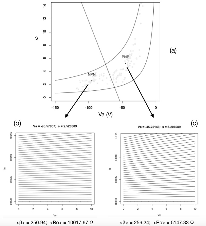
The obtained results are shown in Figure 21(a), which also includes a diluted representation of the devices. Remarkably, all the considered transistors resulted between the two isolines, which correspond to (lower curve) and (upper curve). The oblique line corresponds to the separatrix between the two groups according to the LDA optimality criterion (based on the distance and dispersion of the features of the devices n the two groups). The average values of and are identified for each group. The NPN group has overall variance (trace of the respective intra-class dispersion matrix [7]) equal to while the dispersion obtained for the PNP devices is equal to . This indicates that the used PNP devices have considerably large parameter variation than the NPN transistors.
The centers of mass (averages) of the and of the NPN and PNP groups are also identified in this figure, and the respective theoretical isolines characterizing the electronic operation of the NPN and PNP prototypical devices in the linear operation region are shown as (b) and (c), respectively. Observe the markedly more inclined isolines obtained for the PNP transistors, implying in smaller output resistance. Interestingly, these two prototype characteristic spaces are characterized by similar . However, the prototype PNP device has about twice as large output resistance .
VIII.3 Theoretical THD Analysis Reveals a Surprising Feature of BJTs
In this section, the obtained Early modeling analytical relationships are considered in a theoretical THD analysis. More specifically, we aim at quantifying THD levels in terms of the Early parameters and , as well as their mapping into the space.
We start by deriving some general results regarding THD of signals given in terms of input and output functions. Let the input signal be a perfect sinusoidal , where is the signal amplitude, is its frequency, and is time. In order to determine the THD implied by a system that produces an output signal , where is a generic function, we obtain , calculate its Fourier transform, and apply the traditional THD definition:
| (11) |
where is the RMS voltage of the harmonic of .
Now, the first interesting property to notice is that the THD does not depend on constant terms () or proportionality constants (), i.e.
| (12) |
The second interesting property of THD is that it does not depend on time scalings of the original signal , i.e.:
| (13) |
provided complete periods of are used in both cases.
Now, it has been shown [11] that, for a common emitter with null emitter resistance and the load attached between the collector and of an NPN transistor, we have:
| (14) | |||
| (15) |
A third equation can be added to express the power dissipated:
| (16) |
The THD implied by the mapping of into can be expressed by using Equation 14 and imposing :
| (17) |
By considering the property in Equation 12, we have:
| (18) |
Surprisingly, it can be immediately verified that the current THD of the considered common emitter NPN configuration operating in linear region (Class A), does not depend on , but only on . Property in Equation 13 extends this remarkable result to any input frequency , considering absence of reactive effects.
This result, combined with Equation 7 and the application of numerical Fourier transform over finely sampled signal versions (it does not seem possible to derive aan nalytical expression for the THD in this case), allow us to draw the lines in the where the THD will be constant, as defined by fixed values of . Figure 22 depicts the so obtained results. Given a THD level, determined by the respective Early parameter , the transistors allowing that level will have directly proportional to with a constant of proportionality that decreases in a non-linear fashion with . Among the considered BJTs, the most linear operation — as far as THD in the adopted configuration is concerned, — is allowed by and . The PNP transistors tend to be particularly non-linear in the considered circumstances. Most of the adopted devices resulted comprised between the THD lines ranging from to , which is a relatively large distortion range. In other words, great distortion variation can be potentially implied by not considering the Early parameter of the chosen transistors.

VIII.4 Experimental THD Analysis with Resistive Loads
The complementary pairs having the smallest and largest parameter differences were considered for experiments taking into account the three push pull amplifier configurations discussed in Section II. These two pairs of transistors are (smallest parameter difference) and , respectively. A purely resistive load was adopted throughout, and . The total harmonic distortion, THD (e.g. [5]), was estimated by using a high quality THD analyzer. The input signals consisted of purely sinusoidal waves with peak-to-peak amplitudes . Table 5 presents the THD values (in %) obtained for each configuration of transistor pair and push pull circuit. As could be expected, considerably large THD values were obtained as a consequence of the simplicity of the considered circuits.
In the case of the simplest push pull configuration, implying large cross-over distortion, the THD values tend to decrease with the input voltage amplitude, because the cross-over effect becomes relatively smaller with respect to the total output voltage. As expected, the THD tends to increase with in the diode push pull configuration. A variable trend was observed for the negative feedback circuit.
Remarkably, and with only two exceptions, the THD values obtained in the three types of push pull circuits were smaller in the BJT pair with more similar parameters, namely . The exceptions were observed for the negative feedback configuration for and . These results tend to confirm two important trends, namely that better results are obtained with complementary pairs having similar parameters, and that negative feedback may not be enough to completely eliminate the effects of parameter variability [10].
| Pair (push pull config.) | 1V | 2V | 3V | 4V | 5V |
|---|---|---|---|---|---|
| (simple) | 32.03 | 15.59 | 10.38 | 7.01 | 5.62 |
| (simple) | 34.05 | 17.15 | 11.15 | 7.83 | 6.25 |
| (diodes) | 0.27 | 0.56 | 0.69 | 0.72 | 0.73 |
| (diodes) | 0.62 | 1.03 | 1.15 | 1.05 | 1.03 |
| (neg. feed.) | 0.29 | 0.82 | 0.59 | 0.64 | 0.65 |
| (neg. feed.) | 0.36 | 0.91 | 0.68 | 0.61 | 0.62 |
It is interesting to observe that push pull configurations can be conceptualized as a single device in the Early modeling, which is achieved by reflecting the PNP portion and merging it into the NPN Early diagram in Figure 6. This combined representation is illustrated in Figure 23. The use of complementary pairs with unmatched parameters will imply the two quadrants respective to the NPN and PNP operation to be asymmetric, resulting in larger distortions, as observed in the reported experiments.
IX Concluding Remarks
Reproducibility, stability, and linearity are most desired properties in BJT amplifying circuits. The former property is limited by the inherent large variability of the characteristic parameters of junction transistors, and the latter is a consequence of several effects, including the dependence of the transistor parameters with the operating voltages and currents, intrinsic non-linearities implied by quantum mechanics, as well as circuit design issues (e.g. the cross-over distortion in push pull configurations). Since the introduction of BJTs in the mid 40’s, much effort has been invested in better understanding and controlling the intrinsic properties, often expressed as parameters, of this important class of transistors, responsible for the onset of modern Electronics. Many models of BJTs and circuit configurations have been proposed, several of them involving the current gain or and the collector output resistance . Despite corresponding to quantities of more intuitive applicability and significance, these parameters have an intrinsic limitation in the sense that they constantly depend on the and even under normal circuit operation. So, oftentimes BJTs are characterized in terms of averages of these parameters, or values taken at a specific operation point.
One of the resources that has been applied in order to reduce power consumption in BJT amplifiers involve the application of a complementary pair operating in push pull configuration classes B or AB. This operation can imply in cross-over distortion, which has to be controlled by some effective means such as diode-induced base biasing and negative feedback. The push pull configuration is particularly appealing from the theoretical point of view because of its symmetry and complementarity, which characterize the unified operation of this configuration. This configuration is particularly important because it is often employed as output stage of many off-the-shelf operational amplifiers. One particularly interesting issue with push pull operation is the inherent difference between NPN and PNP devices, which is mostly a consequence of different mobilities in the N and P semiconductors, and geometrical parameters [20, 18]. Therefore, it would be interesting to achieve a better understanding, if possible in simple and intuitive fashion, of the characteristics and variability intrinsic to each of the two main transistors types. Actually, NPN BJTs tend to be more often used in practice than the PNP counterparts as a consequence of differentiating properties between these two categories.
Advances in instrumentation, pattern recognition, image analysis, and transistor modeling have jointly paved the way to more comprehensive integrated studies of semiconductor devices and circuits. In particular, a recently introduced Early modeling for BJTs [11] provided a simple and intuitive framework for investigating devices and circuit configurations. Of special interest is the fact that the two main involved parameters, namely the Early voltage and the proportionality parameter largely do not depend on and during normal circuit operation, being almost constant and intrinsic to each individual BJT. In addition, the Early model provides a simple and elegant geometrical understanding of BJT operation and parameters. In the present work, we used an improved version of the Early modeling approach reported inc̃itecostaearly:2017 in order to investigate the properties of complementary pairs of BJTs. In particular, the estimation of is performed by a voting scheme motivated by the image analysis technique known as the Hough transform, capable of reducing the interference between the isolines. This modification corresponds to the first main contribution of the present work. In addition, we derive relationships between the Early parameters and with the more traditionally applied current gain and output resistance . Because these two latter parameters depend on and , their average value in the operation region had to be taken into account in the derived relationships with the Early parameters. These relationships, which can be adapted to more general operation regions than the first quadrant , constitute another contribution of the present article, which allowed the Early approach and results to be related and interpreted in terms of the more traditional and intuitive parameters and . The whole procedure for estimating the Early parameters, including signal capture, pre-processing, adherence residuals, as well as the numeric estimation procedure were described, discussed and illustrated. The acquisition system, build exclusively for the reported experiments, was also briefly described.
Th reported theoretic-experimental framework was then applied for the characterization of 7 types of complementary BJT pairs, each represented by 10 respective samples, totaling 140 real-world small signal devices. Several interesting results were identified and discussed. When mapped onto the Early space, the real-world devices resulted comprised within a relatively narrow band with increasing values of for larger values of . The NPN and PNP groups of devices resulted markedly separated in the Early space, with the former exhibiting improved linearity at the cost of larger output resistance. The PNP group was also characterized by larger parameter variation, especially in which concerns the proportionality parameter . The region defined by bounding isolines of for constant values of 100 and 400, obtained by using the theoretically derived relationship between the Early parameters and the more traditionally used , was found to neatly contain all the experimental devices mapped in the Early space. These results regarding the two main transistor types constitute another of the main contributions of the present work.
The variability and relationships between the other parameters, namely , and , were also considered and discussed. By incorporating linear discriminante analysis, it was possible to identify an optimal separatrix between the NPN and PNP groups. A prototype NPN-PNP Early space was then derived by combining this separatrix with the 100 and 400 isolines, and the average Early parameters. This space summarizes in an effective and yet comprehensive way the main properties and respective variability of the two main types of BJTs. The theoretical isolines corresponding to the averages obtained for the NPN and PNP groups were also derived and illustrated, corresponding to prototypical isoline respective configurations in the space. Remarkably, the obtained prototype NPN and PNP devices resulted with similar values, but considerably different and , as well as . This suggests that NPN and PNP tend to be, in the average, matched regarding the current gain . The divergence of characteristics would therefore be accounted by differences between the other parameters, such as . The obtained relationships between the Early parameters and and were then used to map the considered real-world BJTs into the space defined by the latter pair of parameters. The results are particularly interesting, with the two groups resulting again almost completely apart, and with PNP still exhibiting larger parameter variability, though to a smaller extent, than NPN counterparts. In addition, as in [10], well-defined groups were obtained for each of the 14 experimentally characterized transistor types, which substantiates the fact that the variability within each transistor type tends to be smaller than the variation between the different types. These results also indicated that the similar cluster orientations obtained in [10] are defined by the narrow curved band occupied by the respective devices in the Early space.
The obtained relationship between the Early parameters and the more commonly used and parameters also allowed the THD of BJTs to be analytically investigated. By using THD properties and the obtained relationships, considering a simplified common emitter configuration [11], a remarkable result, which constitutes another of the main contributions of the present work, was achieve in which the THD, for a fixed circuit configuration, does not depend on , but only on . By mapping the lines defined in the Early space for , it was possible to identify that oblique lines with positive slopes are defined in the more traditional space. Thus, for a fixed THD level indexed by , if a transistor with that level has higher , it will have proportionally higher . The considered BJTs were observed to have their THD levels to vary significantly among the samples of the same transistor type, with interesting practical implications.
To conclude the reported investigation, two hybrid (in the sense of involving transistors from different types) complementary pairs, one with the closest parameter configuration and the other with the most diverging parameters, were taken back to the bench and used in three push pull configurations amplifying sinusoidal signals with progressively increasing voltage amplitudes onto a resistive load. In the greatest majority of cases, the use of the better matched pair led to improved THD values, even in the presence of negative feedback. These results corroborate, at least for the considered devices and circuits, the validity of using complementary transistors with similar parameter values whenever possible. Interestingly, it turns out to be a particularly challenging task because, as indicated in the reported experimental results, NPN transistors tend to occupy rather distinction positions in the Early space, implying in markedly divergent electronic properties.
The efficacy of the reported methodology, as well as the several results obtained regarding NPN and PNP characteristics and parameters variation pave the way to a number of future related works, which are discussed as follows.
First, it would be interesting to extend theoretically and experimentally the reported approaches to other families of transistors, such as FET and MOS, as well as to high frequency and high power BJTs. Also promising would be to experimentally map older device technologies, in particular those based on germanium, in order to compare their parametric features with the more modern silicon counterparts. Preliminary experiments performed by the author, considering an old new stock (NOS) lot of a type of NPN germanium junction transistors, suggested that these devices are characterized by very small values and small values, the latter being comparable to those of silicon PNP devices. Another intriguing question concerns if the Early approach can be eventually applied to other types of amplifiers, such as optical, mechanical, acoustical, etc.
Regarding complementary pairs, it would be of interest to consider, in a similar fashion as in [12], off-the-shelf transistor arrays containing matched NPN and PNP transistors. Further investigations are also required in order to possibly extend the obtained results to other models of transistors operating in different circuit configurations, not to mention transistor arrangements such as Darlington tandem and in parallel. Also, the proposed methodology can be applied to infer the effects of negative feedback in the resulting Early parameters, such as in common emitter and push pull configurations. Of special interest would be the consideration of reactive loads typically found in practice. It is believe that the results reported presently can be directly extended to this type of loads.
It would also be interesting to consider the here identified parametric relationships in terms of conformal mappings [4]. It is also believed that, with simple adaptations, the proposed framework can be extended to the characterization and analysis of sensors and transducers. In this respect, it is believed that interesting experiments can be performed with off-the-shelf optocouplers. Needless to say, all the concepts, methods and results presented in this work can be natural and effectively extended to transistors in integrated circuits at their progressive integration levels. Also, It would be worth investigating in which sense the results reported in this work could be applied to digital electronics, especially concerning the switching time.
At the level of the physics of semiconductors devices, it would be promising to use the reported methods in order to identify possible relationships between the Early parameters and other properties characteristics of PNP and NPN materials. In particular, it would be to check the effects of temperature over the Early parameters.
Several of the above mentioned venues for further research are being currently investigated and results should be reported opportunely. It should be also observed that the Early approach to modeling and characterizing transistors is particularly simple and has good potential for being used for didactic purposes regarding device and circuit theory and practice.
All in all, the Early effect provides a simple and efficient geometrical framework for approaching analog electronic devices and circuits, ranging from discrete devices to VLSI. It remains an additional interesting question, worth of further study, wether the convergence of isolines observed for BJTs (and also other families such as MOSFETs) constitutes a type of universal feature exhibited by most amplifying and modulating devices of several natures and technologies..
Acknowledgments.
Luciano da F. Costa thanks CNPq (grant no. 307333/2013-2) for sponsorship. This work has been supported also by FAPESP grants 11/50761-2 and 2015/22308-2.
References
- [1] D. R Amancio, C. H. Comin, D. Casanova, G. Travieso, O. M. Bruno, F. A. Rodrigues, and L. da F. Costa. A systematic comparison of supervised classifiers. PLOS ONE, 2014.
- [2] H. S. Black. Stabilized feedback amplifiers. Bell System Technical Journal, (1):1–18, 1934.
- [3] W. K. Chen. Feedback Amplifier Theory. World Scientific, 2016.
- [4] R. V. Churchill and J. W. Brown. Complex Variables and Applications. McGraw Hill, 1984.
- [5] R. Cordell. Designing Audio Power Amplifiers. McGraw-Hill, 2011.
- [6] L. da F. Costa, D. Ben-Tzvi, and M. B. Sandler. Performance improvements to the Hough transform. In UK IT Conference, Southampton, UK, March 1990.
- [7] L. da F. Costa and R. M. C. Cesar Jr. Shape Classification and Analysis: Theory and Practice. CRC Press, Boca Raton, 2nd edition, 2009.
- [8] L. da F. Costa and M. B. Sandler. Improving parameter space for Hough transform. Electronics Letters, (2):134–136, 1989.
- [9] L. da F. Costa and M. B. Sandler. CVGIP: Graphical Models and Image Processing, (3):180–191, 1993.
- [10] L. da F. Costa, F. N. Silva, and C. H. Comin. Electrical Engineering, (3):1139, 2017.
- [11] L. da F. Costa, F.N. Silva, and C.H. Comin. An Early model of transistors and circuits, 2017. arXiv preprint arXiv:1701.02269.
- [12] L. da F. Costa, F.N. Silva, and C.H. Comin. A pattern recognition approach to transistor array parameter variance, 2017. arXiv preprint arXiv:1708.00469.
- [13] J.M. Early. Effects of space-charge layer widening in junction transistors. Proceedings of the IRE, (11):1401–1406, 1952.
- [14] P. R. Gray and R. G. Meyer. Analysis and design of analog integrated circuits. John Wiley & Sons, Inc., 1990.
- [15] P.V.C. Hough. Method and means for recognizing complex patterns, December 18 1962. US Patent 3,069,654.
- [16] R. C. Jaeger and T. N. Blalock. Microelectronic Circuit Design. McGraw-Hill New York, 1997.
- [17] R. A. Johnson and D.W. Wichern. Applied multivariate statistical analysis. Prentice Hall, 2002.
- [18] Boylestad R. L and L. Nashelsky. Electronic Devices and Circuit Theory. Pearson, 2008.
- [19] A. Ochoa. Feedback in Analog Circuits. Springer Verlag, 2016.
- [20] G Parker. Introductory Semiconductor Device Physics. Taylor & Francis, 2004.
- [21] G. Raikos and C. Psychalinos. Low-voltage current feedback operational amplifiers. Circuits, Systems & Signal Processing, (3):377–388, 2009.
- [22] M. Riordan and L. Hoddeson. Crystal Fire – The Birth of the Information Age. W. W. Norton & Co., 1997.
- [23] A. Sedra and K. Carless Smith. Microelectronic circuits. Oxford University Press, New York, 1998.
- [24] D. Self. Audio power amplifier design. Taylor & Francis, 2013.
- [25] F.N. Silva, C. H. Comin, and L. da F. Costa. Seeking maximum linearity of transfer functions. Rev. Sci. Instrums., 87(124701), 2016.
- [26] G. E. Tobey. Operational Amplifiers: Design and Applications. McGraw Hill, 1971.
- [27] J Williams. Analog circuit design: art, science, and personalities. Newnes, 1991.