]e1Corresponding author: paolo.cattaneo@pv.infn.it 22 2 †]e2Deceased
The design of the MEG II experiment
Abstract
The MEG experiment, designed to search for the decay at a sensitivity level, completed data-taking in 2013. In order to increase the sensitivity reach of the experiment by an order of magnitude to the level of for the branching ratio, a total upgrade, involving substantial changes to the experiment, has been undertaken, known as MEG II. We present both the motivation for the upgrade and a detailed overview of the design of the experiment and of the expected detector performance.
1 Introduction
1.1 Status of the MEG experiment in the framework of charged Lepton Flavour Violation (cLFV) searches
The experimental upper limits established in searching for cLFV processes with muons, including the decay, are shown in Fig. 1 versus the year of the result publication. Historically, the negative results of these experiments led to the formulation of the Standard Model (SM) of elementary particles interactions, in which lepton flavour conservation was empirically included. During the past 35 years the experimental sensitivity to the decay has improved by almost three orders of magnitude, mainly due to improvements in detector and beam technologies. In particular, ‘surface’ muon beams (i.e. beams of muons originating from stopped s decay in the surface layers of the pion production target) with virtually monochromatic momenta of , offer the highest muon stop densities obtainable at present in low-mass targets, allowing ultimate resolution in positron momentum and emission angle and suppressing the photon background production.
The signal of the two-body decay at rest can be distinguished from the background by measuring the photon energy , the positron momentum , their relative angle and timing with the best possible resolutions.
The background comes either from radiative muon decays (RMD) in which the neutrinos carry away a small amount of energy or from an accidental coincidence of an energetic positron from Michel decay with a photon coming from RMD, bremsstrahlung or positron annihilation-in-flight (AIF) . In experiments using high intensity beams, such as MEG, this latter background is dominant.
The keys for search experiments achieving high sensitivities can be summarised as
- 1.
A high intensity continuous surface muon beam to gain the data statistics with minimising the accidental background rate (cf. Eq. (2) below).
- 2.
A low-mass positron detector with high rate capability to deal with the abundant positrons from muon decays.
- 3.
A high-resolution photon detector, especially in the energy measurement, to suppress the high-energy random photon background.
The MEG experiment [1] at the Paul Scherrer Institute (PSI, Switzerland) uses one of the world’s most intense (maximum rate higher than continuous surface muon beams, but, for reasons explained in the following, the stopping intensity is limited to . The muons are stopped in a thin () polyethylene target, placed at the centre of the experimental set-up which includes a positron spectrometer and a photon detector, as shown schematically in Fig. 2.

The positron spectrometer consists of a set of drift chambers and scintillating timing counters located inside a superconducting solenoid COBRA (COnstant Bending RAdius) with a gradient magnetic field along the beam axis, ranging from at the centre to at either end, that guarantees a bending radius of positrons weakly dependent on the polar angle. The gradient field is also designed to remove quickly spiralling positrons sweeping them outside the spectrometer to reduce the track density inside the tracking volume.
The photon detector, located outside of the solenoid, is a homogeneous volume () of liquid xenon (LXe) viewed by 846 UV-sensitive photomultiplier tubes (PMTs) submerged in the liquid, that read the scintillating light from the LXe. The spectrometer measures the positron momentum vector and timing, while the LXe photon detector measures the photon energy as well as the position and time of its interaction in LXe. The photon direction is measured connecting the interaction vertex in the LXe photon detector with the positron vertex in the target obtained by extrapolating the positron track. All the signals are individually digitised by in-house designed waveform digitisers (DRS4) [2].
The number of expected signal events for a given branching ratio is related to the rate of stopping muons , the measurement time , the solid angle subtended by the photon and positron detectors, the efficiencies of these detectors () and the efficiency of the selection criteria :33 3 An usual selection criterion is to choose 90% efficient cuts on each of the variables (, , , ) around the values expected for the signal: this criterion defines the selection efficiency to be . This kind of analysis in which one counts the number of events within some selection cuts and compares the number found with predictions for the background is named “box analysis”. MEG/MEG II adopt more refined analyses which take into account the different distributions of (, , , ) for background and signal type events by using maximum likelihood methods.
| (1) |
The single event sensitivity (SES) is defined as the for which the experiment would see one event. In principle the lowest SES, and therefore the largest possible , is desirable in order to be sensitive to the lowest possible . The number of accidental coincidences , for given selection criteria, depends on the experimental resolutions (indicated as in Eq. 2) with which the four relevant quantities (, , , ) are measured. By integrating the RMD photon and Michel positron spectra over respectively the photon energy and positron momentum resolution intervals, it can be shown that:
| (2) |
Due to the quadratic dependence on , the accidental coincidences largely dominate over the background coming from RMD (which is linearly dependent on ). It is clear from Eqs. (1) and (2) that, for fixed experimental resolutions, the muon stopping rate cannot be increased arbitrarily but must be chosen in order to keep a reasonable signal to background ratio.
The current published MEG limits of at 90% confidence level (CL), based on the full data-set [3] is currently the most stringent limit on this decay. Given that the background (accidental) extends into the signal region, only a limited gain in sensitivity could be achieved with further statistics, hence data-taking ceased in 2013, allowing the upgrade program to proceed with full impetus.
Other cLFV channels, complementary to and being actively pursued are: , , and ( or ). In the conversion experiments, negative muons are stopped in a thin target and form muonic atoms. The conversion of the muon into an electron in the field of the nucleus results in the emission of a monochromatic electron of momentum , depending on the target nucleus used. Here the backgrounds to be rejected are totally different from the case. The dominant examples are muon decay-in-orbit and those correlated with the presence of beam impurities, such as pions. In order to reduce these backgrounds the experiments planned at Fermilab (Mu2e) [4, 5] and J-PARC (COMET [6, 7] and DeeMe [8]) will use pulsed proton beams to produce their muons.
Since muonic atoms have lifetimes ranging from hundreds of nanoseconds up to the free muon lifetime at low Z, the conversion electrons are therefore searched for in the intrabunch intervals.
The COMET collaboration plans to start the first phase of the experiment in 2018 with a sensitivity reach better than followed by the second phase aiming for a goal sensitivity of , while the Mu2e experiment is foreseen to start in 2021 with a first phase sensitivity goal of . These experiments can in principle reach sensitivities below [9, 10].
The decay search is being pursued in a new experiment, proposed at PSI: Mu3e [11]. This plans a staged approach to reach its target a sensitivity of . The initial stage involves sharing part of the MEG beam line and seeks a three orders-of-magnitude increase in sensitivity over the current limit, its goal being . The final stage foresees muon stopping rates of the order of .
and will be explored by the Belle II experiment at SuperKEKB [12, 13] and a proposed experiment at the super Charm-Tau factory [14, 15] where sensitivities of the order of to the branching ratios for these channels are expected.
A comparison between the sensitivity planned for MEG II and that envisaged for the other above mentioned cLFV processes will be discussed in the next section after a very short introduction to cLFV predictions in theories beyond the SM.
1.2 Scientific merits of the MEG II experiment
Although the SM has proved to be extremely successful in explaining a wide variety of phenomena in the energy scale from sub- to , it is widely considered a low energy approximation of a more general theory. One of the attractive candidates for such theory is the grand-unified theory (GUT) [16] which unifies all the SM gauge groups into a single group as well as quarks and leptons into common multiplets of the group. In particular, the supersymmetric version (SUSY-GUT) has received a great amount of attention after the LEP experiments showed that a proper unification of the forces can be achieved at around a scale if SUSY particles exist at a scale [17]. The search for TeV-scale SUSY particles has been one of the goals of the LHC program. Results so far have been negative for masses up to [18, 19].
The experimentally measured phenomenon of neutrino oscillations [20, 21, 22] requires an extension of the SM. It demonstrates that lepton flavour is violated, and neutrinos have masses but they are orders of magnitude smaller than those of quarks and charged leptons. An appealing extension of the SM consists in introducing Majorana masses for neutrinos to naturally account for the tiny neutrino masses via the seesaw mechanism [23, 24, 25, 26]. This approach predicts the existence of heavy right-handed Majorana neutrinos44 4 This is called Type-I seesaw. Other types of the seesaw mechanism have also been invented; see [27] for a review. in the range of . This ultra-high mass scale may be indicative of their connection to SUSY-GUT (e.g. all the SM fermions plus the right-handed neutrino in a generation can fit into a single multiplet in SO(10) GUT). The Majorana neutrinos violate the lepton number, and may account for the matter–antimatter asymmetry in the Universe [28].
It is generally difficult to detect, even indirectly, the effects of such ultra-high energy scale physics. However, the situation changes with SUSY, and cLFV signals provide a general test of SUSY-GUT and SUSY-seesaw as discussed below.
It is well known that cLFV is sensitive to SUSY [29, 30, 31]; in fact the parameter space for the minimal SUSY extension of the SM (MSSM) has largely been constrained by flavour- and CP-violation processes involving charged leptons and quarks [32, 33, 34, 35]. These experimental observations lead to considering special mechanisms of SUSY breaking, requiring e.g. the universal condition of SUSY particles’ masses at some high scale. It was however shown that mixing in sleptons emerges unavoidably at low energy in SUSY-GUT [36] and SUSY-seesaw [37] models even if the lepton flavour is conserved at high scale. This is because flavour-violation sources, i.e. at least the quark and/or neutrino Yukawa interactions, do exist in the theory and radiatively contribute to the mass-squared matrices of sleptons during the evolution of the renormalisation-group equation.55 5 This effect is enhanced by large Yukawa couplings. The large top Yukawa coupling does it in SUSY-GUT models. The neutrino Yukawa couplings can be the same order as those for quarks and charged leptons in the seesaw mechanism. In particular, in SO(10) GUT, neutrino Yukawa couplings are related to up-type ones and at least one of them should be as large as the top one [38]. As a result, is predicted at an observable level [39, 40, 41, 42, 43, 44, 45, 46]. This theoretical framework motivated the MEG and MEG II experiment.
In order to appreciate this, we recall that the SM, even introducing massive neutrinos, practically forbids any observable rate of cLFV () [47, 48]. Processes with cLFV are therefore clean channels to look for possible new physics beyond the SM, for which a positive signal would be unambiguous evidence.
Over the last five years, two epoch-making developments took place in particle physics: the discovery of Higgs boson [49, 50] and the measurement of the last unknown neutrino mixing angle [51, 52, 53, 54]. The mass of Higgs boson at [55], rather light, on one hand supports the SUSY-GUT scenario since it is actually in the predicted region [56]. On the other hand, it is relatively heavy in MSSM and suggests, together with the null results in the direct searches at LHC, that the SUSY particles would be heavier than expected. This implies that a smaller is expected because of the approximate dependence . This might explain why MEG was not able to detect the signal as well as why other flavour observables, particularly [57] and [58], have been measured to be consistent with the SM so far. In contrast, the observed large mixing angle [22] suggests higher in many physics scenarios such as SUSY-seesaw.
Updated studies of SUSY-GUT/seesaw models taking those recent experimental results into account show that – is possible up to SUSY particles’ masses around [59, 60, 61, 62, 63, 64, 65, 66, 67], well above the region where LHC (including HL-LHC) direct searches can reach. In addition, cLFV searches are sensitive to components which do not strongly interact (e.g. sleptons and electroweakinos in MSSM) and thus are not much constrained by the LHC results. Considering these situations, further exploration of the range in coincidence with the 14- LHC run provides a unique and powerful probe, complementary and synergistic to LHC, to explore new physics.
So far, we discussed SUSY scenarios, the main motivation of MEG II, but many other scenarios, such as models with extra-dimensions [68, 69, 70], left-right symmetry [71, 72, 73, 74], leptoquarks [75, 76, 77, 78], and little Higgs [79, 80, 81, 82], also predict observable rates of within the reach of MEG II.
Comparison between different transition processes can be done model independently by an effective-field-theory approach. Considering new physics, cLFV processes are generated by higher-dimensional operators; the lowest one that directly contributes to is the following dimension-six (dipole-type) operator,
| (3) |
where is the vacuum expectation value of the Higgs field and is the field-strength tensor of photon. This operator also induces and via the propagation of a virtual photon. There are several other dimension-six operators which cause the transitions, and their amplitudes to each of the three processes are model-dependent.66 6 Recent effective-field-theory analyses have shown that those operators valid at some high scale mix at the low energy scale where the experiments take place via the evolution of renormalisation-group equation [83]. Due to this mixing effect as well as higher order contributions, the limit on provides severe constraints also on operators other than (3).
In many models, especially most of SUSY models including the above mentioned SUSY-GUT/seesaw models, the operator (3) dominates the transitions. In such a case, the following relations hold independently of the parameters in the models [84, 85]:
| (4) | ||||
| (5) |
Therefore, a search for with a sensitivity of , which is the target of MEG II, with a much shorter timescale and a far lower budget than other future projects, is competitive not only with the second phase of the Mu3e experiment [11] but also with the COMET [6] and Mu2e [5] experiments. On the other hand, in case of discovery, we can benefit from a synergistic effect by the results from these experiments, providing a strong model-discriminant power; any observations of discrepancy from the relations (4) (5) would suggest the existence of the contributions from operators other than (3).
The comparison between and processes is more model dependent. In the SUSY-seesaw models with and without GUT relations, the ratio roughly ranges from .77 7 and are typically orders of magnitude smaller than in these models. Therefore, the present MEG bound on already sets strong constraints on to be measured in the coming experiments [13]. If will be detected in these experiments without a discovery of in MEG II, such models will be strongly disfavoured.
We finally note that MEG II will represent the best effort to address the search of the rare decay with the available detector technology coupled with the most intense continuous muon beam in the world. Experience shows that to achieve any significant improvement in this field several years are required (more than one decade was necessary to pass from MEGA to MEG) and therefore we feel committed to push the sensitivity of the search to the ultimate limits.
1.3 Overview of the MEG II experiment
The MEG II experiment plans to continue the search for the decay, aiming for a sensitivity enhancement of one order of magnitude compared to the final MEG result, i.e. down to for . Our proposal for upgrading MEG [86] was approved by the PSI research committee in 2013 and then, the details of the technical design has been fixed after intensive R&D and is reported in this paper.
The basic idea of the MEG II experiment is to achieve the highest possible sensitivity by making maximum use of the available muon intensity at PSI with the basic principle of the MEG experiment but with improved detectors. A schematic view of MEG II is shown in Fig. 3.

A beam of surface is extracted from the E5 channel of the PSI high-intensity proton accelerator complex, as in MEG, but the intensity is increased to the maximum. After the MEG beam transport system, the muons are stopped in a target, which is thinner than the MEG one to reduce both multiple Coulomb scattering of the emitted positrons and photon background generated by them. The stopping rate becomes , more than twice that of MEG (see Sect. 2).
The positron spectrometer uses the gradient magnetic field to sweep away the low-momentum . The COBRA magnet is retained from MEG, while the positron detectors inside are replaced by new ones. Positron tracks are measured by a newly designed single-volume cylindrical drift chamber (CDCH) able to sustain the required high rate. The resolution for the momentum vector is improved with more hits per track by the high density of drift cells (see Sect. 4). The positron time is measured with improved accuracy by a new pixelated timing counter (pTC) based on scintillator tiles read out by SiPMs (see Sect. 5). The new design of the spectrometer increases the signal acceptance by more than a factor 2 due to the reduction of inactive materials between CDCH and pTC.
The photon energy, interaction point position and time are measured by an upgraded LXe photon detector. The energy and position resolutions are improved with a more uniform collection of scintillation light achieved by replacing the PMTs on the photon entrance face with new vacuum-ultraviolet (VUV) sensitive SiPMs (see Sect. 6).
A novel device for an active background suppression is newly introduced: the Radiative Decay Counter (RDC) which employs plastic scintillators for timing and scintillating crystals for energy measurement in order to identify low-momentum associated to high-energy RMD photons (see Sect. 7).
The trigger and data-acquisition system (TDAQ) is also upgraded to meet the stringent requirements of an increased number of read-out channels and to cope with the required bandwidth by integrating the various functions of analogue signal processing, biasing for SiPMs, high-speed waveform digitisation, and trigger capability into one condensed unit (see Sect. 8).
In rare decay searches the capability of improving the experimental sensitivity depends on the use of intense beams and high performance detectors, accurately calibrated and monitored. This is the only way to ensure that the beam characteristics and the detector performances are reached and maintained over the experiment lifetime. To that purpose several complementary approaches have been developed with some of the methods requiring dedicated beams and/or auxiliary detectors. Many of them have been introduced and commissioned in MEG and will be inherited by MEG II with some modifications to match the upgrade. In addition new methods are introduced to meet the increased complexity of the new experiment.
Finally, the sensitivity of MEG II with a running time of three years is estimated in Sect. 9.
2 Beam line
2.1 MEG beam line layout
The main beam requirements for a high rate, high sensitivity, ultra-rare decay coincidence experiment such as MEG are:
- •
high stopping intensity () on target with high transmission optics,
- •
small beam spot to minimise the stopping target size,
- •
large momentum-byte (FWHM) with an achromatic final focus, yielding an almost monochromatic beam with a high stop density for a thin target,
- •
minimal and well separated beam-correlated backgrounds such as positrons from Michel decay or -decay in the production target or decay particles from along the beam line and
- •
minimisation of material budget along the beam line to suppress multiple scattering and photon production, use of vacuum or helium environments as far as possible.
Coupling the MEG COBRA spectrometer and LXe photon detector to the E5 channel, which ends with the last dipole magnet ASC41 in the shielding wall, is achieved with a Wien-filter (cross-field separator) and two sets of quadrupole triplet magnets, as shown in Fig. 4. These front-elements of the MEG beam line allow a maximal transmission optics through the separator, followed by an achromatic focus at the intermediate collimator system. Here an optimal separation quality between surface muons and the eight-fold higher beam positron contamination from Michel positrons or positrons derived from -decay in the target and having the correct momentum, can be achieved (see Fig. 5) [1]. The muon range-momentum adjustment is made at the centre of the superconducting beam transport solenoid BTS where a Mylar® degrader system is placed at the central focus to minimise multiple scattering. The degrader thickness of takes into account the remaining material budget of the vacuum window at the entrance to the COBRA magnet and the helium atmosphere inside, so adjusting the residual range of the muons to stop at the centre of a thick polyethylene target placed at to the axis.
The residual polarisation of the initially 100% polarised muons at production has been estimated by considering depolarising effect at production, during propagation and due to moderation in the stopping target. The net polarisation is seen in the asymmetry of the angular distribution of decay Michel positrons from the target. The estimate is consistent with measurements made using Michel positrons at the centre of the COBRA spectrometer [87], where the energy-dependent angular distributions were analysed. A high residual polarisation of was found, with the single largest depolarising contribution coming from the cloud muon content of the beam. These are muons derived from pion decay-in-flight in and around the target and inherently have a low polarisation due to the widely differing acceptance kinematics. The cloud muon content in the surface muon beam was derived from measurements where the muon momentum spectrum was fitted with a constant cloud muon content over the limited region of the kinematic edge of the spectrum at . This was cross-checked against measurements at using a negative muon beam. In this case, there are no such surface muons (due to the formation of pionic atoms on stopping) and hence a clear cloud muon signal can be measured. When comparing the cross-sections and the kinematics of pions of both charge signs consistency is found, with a ratio of % of negative cloud muons to surface muons at . This situation is not expected to change significantly for MEG II, apart from the slightly higher divergences expected due to the increased and a possible difference in the polarisation quenching properties of the target material in a magnetic field [88], which is still under investigation.

2.2 Upgrade concept

The increased sensitivity sought in MEG II will partially be realised by the full exploitation of the available beam intensity and partially by the increased detector performances, allowing the most significant contribution to the background from overlapping accidental events, to be managed, at the level of an order of magnitude higher sensitivity for the experiment. As outlined in Sect. 1.1 the accidental background has a quadratic dependence on the muon beam stopping rate, whereas the signal is directly proportional to the stopping rate. This puts stringent limits on the material budget and the suppression of beam-correlated backgrounds in the beam line, while having to allow for the flexibility and versatility of different beam modes required for calibration purposes. The three main modes required are:
For MEG II, the beam line components and optics will stay the same, apart from the introduction of extra beam monitoring tools (cf. Sect. 2.3.2). However, the increased muon rate for MEG II, while maintaining the high transmission optics, can only be achieved by an increase in the momentum-byte i.e. by means of opening the E5 channel momentum slits to their full extent. An increased however, implies an increased range straggling of the beam. A study undertaken for the MEG II upgrade proposal [86] looked at various beam/target scenarios comparing the use of a surface muon beam of (mean range ) to that of a sub-surface beam of (mean range ). As the name implies, these are muons with a unique momentum of from stopped pion decay, which are selected from deeper within the target and lose some of their energy on exiting.
The potential advantage of such a sub-surface beam is then the reduced range straggling which is comprised of two components (cf. Eq. (6)). The first factor from energy-loss straggling of the intervening material, which at these momenta amounts to about 9% (FWHM) of the range [89] and the second from the momentum-byte . However, the range and the straggling vary most strongly with momentum, being proportional to , where ‘’ is a material constant,
| (6) |
Therefore, the most efficient way to reduce the range straggling is by reducing the momentum rather than the .

A momentum change has a direct impact on the target thickness, which is a balance between maximising the stop density and minimising the multiple scattering of the out-going Michel positrons and the photon background produced in the target. Furthermore, the surface muon rate also decreases with and therefore ultimately limits how low one can go down in momentum. This behaviour is shown in Fig. 6, where the measured muon momentum spectrum is fitted with a power-law, folded with a Gaussian momentum resolution equivalent to the momentum-byte, plus a constant cloud muon content. The blue and the red (truncated) boxes show the momentum acceptance for the surface/sub-surface beams, corresponding respectively to (/) . The optimal momentum yielding the highest intensity within the full momentum-byte is centred around . For each data-point the whole beam line must be optimised. The upgrade study [86] investigated various combinations of beam momentum and target parameters such as thickness which varied between and orientation angle varying between . This resulted in only one really viable solution that could yield the required muon stopping intensity of suitable for achieving the goal sensitivity within a measuring period of years: a surface muon beam of with a polyethylene target of thickness, placed at an angle of to the axis.
A sub-surface beam solution was only able to meet the criteria by scaling-up the target thickness to , which negated the principle. Hence the baseline solution chosen for MEG II was the surface muon beam solution due to the thinner target and higher achievable rate as well as its beneficial impact on the resolutions and background.
2.3 Beam monitoring
Two new detectors have been developed to measure the beam profile and rate: the sampling scintillating fibre beam monitoring (sampling SciFi) mounted at the entrance to the spectrometer and the luminophore foil detector (CsI on a Mylar support) coupled with a CCD camera installed at the intermediate focus collimator system.
2.3.1 The sampling SciFi beam monitoring detector
This detector is a quasi non-invasive, high rate sustainable beam monitoring tool, able to provide beam rate, profile measurements and particle identification in real time. It is based on scintillating fibres (SciFi) coupled to SiPMs; the usage of SiPMs allows for a detector able to work in high magnetic fields.
It consists of a grid of two orthogonal fibre layers: one with the fibres running along the -axis and the other with the fibres along the -axis. The detector is expected to be located at the end of the vacuum beam line, just in front of the spectrometer. A movable configuration allows the remote removal/insertion of the detector into the beam.
Figure 7 shows the built and tested full scale prototype. We used Saint-Gobain BCF-12, double-cladding fibres [90], each one independently coupled at both ends to Hamamatsu S13360-1350CS SiPMs (with an active area of and a pixel size of ) [91]. The relative distance between adjacent fibres mounted in the same layer is equal to , a pitch which satisfies the requirements for a precise measurement of the beam profile and rate. Furthermore a large detector transparency (where particles hitting the fibres / total incident particles) is achieved with a relatively small number of channels (). In fact for this prototype we mounted 21 fibres per layer giving a total number of 84 channels. The signals are sent to the TDAQ prototype (see Sect. 8) that includes also the preamplifiers (with adjustable gain up to 100, which is what we used here) and the power supplies for the SiPMs (operated at ). The trigger used for the beam profile and rate measurements is the “OR” of all the “AND”s of the SiPMs coupled to the same fibre, with a common threshold for all channels photoelectrons.

Figure 8 shows the beam profile as measured with the detector mounted along the E5 beam line. The incident particles are positive muons with an initial momentum of , after having left the Mylar window at the end of the vacuum beam line and travelling some in air before traversing the of Tedlar® used as a light tight shield. The corresponding total rate and beam profiles were and , respectively. These measured numbers are consistent to within 5% or better with those provided by our “standard” beam monitoring tools (methods based on a 2D x-y scanner using a large depletion layer APD or a pill scintillator coupled to a miniature PMT). One of the most attractive features of this detector is its capability of providing the full beam characterisation in just tens of seconds with all the associated benefits (faster beam tuning, real time feedback about a malfunctioning of the beam/apparatus, reduced systematic uncertainties etc.).
Figure 9 shows the detected charge associated with positrons of and stopping muons in the fibres. A clear separation between the positrons (which are minimum ionising particles m.i.p.) and the low energy muons can be seen.
Figure 10, finally, shows the capability of the detector to distinguish between high momentum particles () by plotting the measured charge associated to them versus their time-of-flight (the radio frequency of the main accelerator is used as a time reference). From left to right we have positrons, pions and muons.
2.3.2 An ultra-thin CsI(Tl) luminophore foil beam monitor
A new in-situ, high rate and non-destructive beam monitoring system based on a thin CsI(Tl) scintillation foil (luminophore) and a CCD camera system has been developed for MEG II. Initial tests as an external device able to measure both the beam intensity as well as giving a quantitative measure of the beam spot size have led to a permanent installation incorporated into the beam line vacuum at the MEG intermediate focus collimator system.
The advantages of such a system over the standard MEG pill-scintillator 2D x-y scanner system are four-fold: in-situ, non-destructive measurement of the beam characteristics, no dismantling of beam line components necessary, as in the case of the pill-scintillator scanner system; in vacuum measurement, no corrections needed for multiple scattering in the vacuum window or air; comparatively fast measurement, multiple exposures each of compared with a pill-scintillator 2D “cross-scan” of or a 2D “raster-scan” of ; continuous monitoring possible allowing online centring in the event of beam steering due to changes of the proton beam position on the muon production target E.
2.3.2.1 CsI(Tl) foils and CCD camera system
CsI(Tl) is a well known and common inorganic scintillator with a relatively high light yield at more than of deposited energy. The peak emission of CsI(Tl) is approximately and well suited for use in visible light imaging systems such as a CCD. The scintillation light decay constants () are rather long compared to fast organic scintillators though not problematic for this application due to the much longer exposure times.
Four foils were constructed using a Lavsan (Mylar® equivalent) base structure, where a thin layer of CsI(Tl) was applied using chemical vapour deposition. The precise CsI(Tl) layer thickness was varied between and , allowing for the comparison and possible optimisation of layer thickness.
The imaging system used was a Hamamatsu ORCA FLASH4.0 camera providing 4.19 megapixels along with pixel depth. An internal Peltier cooling device as well as an external water cooling system allow the sensor temperature to be reduced to and hence significantly reducing the thermal noise. The sensor’s peak quantum efficiency matches well to the CsI(Tl) peak emission near .
2.3.2.2 Beam image analysis
Beam profile imaging consists of multi-frame (typically 10) exposures each of length together with an equivalent set of background exposures taken with the beam-blocker closed, enabling stray ambient light and the inherent thermal noise of the sensor to be eliminated on subtraction.
All signal and background images are first summed and averaged and then subtracted to generate a calibrated signal image, from which a central region of interest is selected. This image is then fitted using a 2D correlated Gaussian function to obtain the beam position and widths in and as well as their correlations. The summed image intensity is normalised by the total proton current during the exposure period. The current measurement is initiated by a simultaneous external trigger of the proton signal scalar and the camera shutter. A typical image after processing is shown in Fig. 11.

2.3.2.3 Beam width
A comparison of the beam spots as measured by the pill-scintillator to those obtained from projections of the luminophore foil image are shown in Fig. 12 with good agreement within the fit widths. The difference in centroids is due to the difference in alignment between the two setups.


The spatial resolution of the luminophore foil system was determined by placing an Al grid just upstream of the foil, while irradiating with the muon beam. The grid edges of the resultant picture image, when fitted with a step-function convoluted with a Gaussian resolution function, yield an upper limit on the combined foil, camera and beam resolution of which includes beam divergence and range straggling effects, so that the intrinsic spatial resolution of the foil is much smaller.
2.3.2.4 Beam intensity
A beam intensity comparison between the luminophore system and the pill-scintillator system was made by symmetrically opening the E5 FS41L/R slit system in small steps, so scanning the full beam intensity over an order of magnitude. The comparative plot of relative intensity normalised to the proton beam intensity is shown in Fig. 13. Good agreement can be seen at the 5 level which can be understood as being due to the difference in technique. The pill-scintillator measurement samples only a diameter portion of the beam on the beam-axis, whereas the luminophore samples the entire beam spot which changes in size with slit opening, at the 10 level over the entire range.

2.3.2.5 Beam line setup
The initially developed external system has since been incorporated into the beam line vacuum as part of the intermediate focus collimator system shown in Fig. 14. The foil frame is attached to a drive shaft and pulley system that allows the foil to be rotated in and out of the beam while under vacuum. A calibration grid is attached to the surface of the frame to allow for a pixel-to-millimetre conversion. The foil and frame are viewed inside the beam pipe, under vacuum and imaged with the CCD camera via a mirror system and glass window on a side port. The interior of the vacuum pipe can be illuminated with a UV LED to conduct calibration measurements of the foil and CCD system within the light-tight region.

An example of the usefulness of such a system can be seen in Fig. 15, which shows the separation quality between muon and positron beam spots imaged at the collimator system with the luminophore foil. The separation quality has purposely been reduced by adjusting the parameters of the Wien filter in order that both spots can be seen simultaneously on the picture. The use of the luminophore allows a calibration of the spatial separation to be made effectively online.

2.3.2.6 Conclusions
Thin CsI(Tl) luminophore foils offer fast, in-situ beam monitoring possibilities, with negligible impact on beam rate and emittance. The foils combined with a cooled camera system with sufficient resolution reproduces beam profile and rate measurements conducted with the scanning pill-scintillator. Full 2D beam measurement can be made approximately ten times faster while providing long-term non-destructive beam information. Furthermore, it allows a direct measure of beam parameters without the need for multiple scattering corrections due to air or vacuum windows and allows direct feedback on external influences on the beam position or intensity.
3 Target
The basic requirements for a MEG stopping target are six-fold:
- •
a high muon stopping density over a limited axial region centred on the COBRA fiducial volume,
- •
minimisation of multiple scattering for the outgoing positrons,
- •
minimisation of photon conversions from RMD in the target,
- •
minimisation of positron AIF or bremsstrahlung with photons entering the detector acceptance,
- •
allow reconstruction of the positron decay vertex and initial direction at the vertex, onto the target plane and
- •
mechanically stable with good planarity and remotely movable for compatibility with calibrations requiring other targets.
Owing to the thinner target, smaller angle for MEG II and the increased , the remaining variable material budget consisting of degrader and COBRA helium environment, must then be matched to give an optimal residual range at the target. Figure 16 shows the simulation results for the optimal stopping efficiency versus degrader thickness for the previous MEG thick polyethylene target. Two different He-concentrations are shown, from which can be seen that 1% of air is equivalent to of Mylar.

For MEG II a separate target study was also undertaken to examine the material possibilities for a target equivalent to the baseline polyethylene (CH2) target, placed at to the axis. The resulting set of candidate targets are listed in Table 1 below. Since the material thickness for each target is equivalent in terms of the surface density , the residual range and hence the degrader thickness is therefore also the same.
| Material | Degrader | Thickness | Thickness | Inclination | Density | Stop Efficiency | Multiple Scattering | |
|---|---|---|---|---|---|---|---|---|
| () | () | (X0) | (deg) | () | (%) | () | ||
| [] | [] | |||||||
| CH2 | 350 | 140 | 15.0 | 0.893 | 83 | 52.0 | 3.0 | |
| Be | 350 | 90 | 15.0 | 1.848 | 83 | 49.3 | 2.9 | |
| Mylar | 350 | 100 | 15.0 | 1.390 | 84 | 58.5 | 3.4 | |
| Scint. PVT | 350 | 130 | 15.0 | 1.032 | 84 | 54.5 | 3.2 | |
| Diamond | 350 | 40 | 15.0 | 3.515 | 81 | 56.8 | 3.3 | |
The main properties affecting tracking and background production, as well as the target stopping efficiency show that there are no dramatic differences between the candidates, with multiple scattering estimates varying less than 10% from the average, while the equivalent thickness in radiation lengths varies by about 15% from the average. A separate background study to estimate the number of background photons with energy produced in the fiducial volume of COBRA per incident muon and entering the LXe photon detector gave values between for the scintillation target and for the Mylar target. The equivalent simulated optimised stopping efficiency in the case of the MEG II polyethylene target is shown in Fig. 17.

Table 1 shows that different materials outperform each other in different categories. In general, the beryllium target shows an overall good performance, though from the thickness and size required, as well as from the safety aspects it is not favoured. Diamond, which is mechanically stable and known to be more radiation tolerant has the smallest radiation length, as well as having scintillation properties. However, it is currently not commercially available in the size required for a MEG II target. The scintillation target (BC400B) from Saint-Gobain lies in the mid-range of the performance span, though with the lowest number of accepted background photons per muon of all targets. A very important and added advantage over the other non-scintillating targets is, the possibility of non-destructive beam intensity and profile measurements, using a CCD camera and optical system. This would allow corrections, caused by proton beam shifts on the main pion production target, to be made to the beam centring on the MEG muon target during data-taking. Two prototype targets have so far been implemented for the Pre-Engineering Runs 2015/16, a polyethylene (PE) and a polyvinyltoluene (PVT) one. The prototype scintillation target (PVT) is seen in Fig. 18.
3.1 Scintillation target prototype

Figure 18 shows the two sides of the prototype target used in the 2016 Pre-Engineering Run, the downstream CCD viewing side has a calibration grid as part of the frame to ensure a correct perspective transformation of the beam image. The frame is a sandwich of carbon-fibre and Rohacell foam ensuring a lightweight construction and strength, as can be seen from the lower image in Fig. 18 (left). The fiducial size of the scintillator, excluding the frame is .
The bare setup including CCD camera, lens and thin Mylar mirror system placed away from the target, on the downstream-side (DS) of the COBRA magnet is shown in Fig. 18 (right). Analysed background subtracted, perspective corrected and 2D Gaussian fitted beam images (see Fig. 19) show that even with a non-ideal CCD camera (no cooling), and exposures of in a strong gradient magnetic field of several , comparable results, at the sub-millimetre level, to the usual 2D APD “raster scans” performed at the centre of COBRA, can be obtained, in a fraction of the time. Furthermore, it was demonstrated that the beam intensity could be measured over the range of a factor of 50 and reproduce results measured independently with the “pill scintillator” scanner system as shown in Fig. 20. The measurements were made by adjusting the opening of the FS41L/R momentum slits of the channel, so changing the intensity. Good agreement is seen.


Finally, a first radiation damage study was also undertaken during the 2016 run with about integrated, corresponding to an integrated dose of (). A loss in light yield was seen, though less than expected [92], which may be understood by the way in which the scintillation light is collected namely, through the very thin scintillator thickness thereby being less sensitive to attenuation. A fit to the data with an exponential decay law gives a decay constant of as shown in Fig. 21. Extrapolating this to the longest MEG beam run of 2012 at the MEG II beam intensity as measured above, would lead to a light yield of % at the end of a 1-year period however, still yielding measurable profiles and intensities as demonstrated above. Normalising UV-LED measurements would be however required for a corrected intensity measurement. Furthermore, this would necessitate a new target for each year. Further radiation tests are envisaged to study the effect on the mechanical properties such as planarity, before a final decision on the target material is taken. A new CCD camera system for imaging the beam on target has now been procured, including cooling and a mechanical shutter which should significantly improve the image quality and the analysis procedure.

3.1.1 Target alignment
An important consideration for the target implementation is the accurate knowledge of the target position, in particular the knowledge of the target planarity and its perpendicular distance from its nominal position. Errors in this coordinate introduce a systematic error in the positron direction at the target due to the error in the path length of the curved positron trajectory projected on to the target plane. An offset of in the target plane introduces a systematic error in the positron -angle of , comparable to the angular resolution achieved by MEG [3]. In MEG, this position was monitored by imaging small holes in the target foil. This monitoring was statistics limited in its ability to monitor deformation of the target foil during the run; lack of precise target position and shape information introduced a significant contribution to the systematic uncertainties in the positron angle measurement. With the anticipated improved angular resolution in MEG II, improved monitoring of the target position and shape is required, with a goal of monitoring the target planarity and transverse position to a precision and the axial position to precision .
It is envisaged, as in MEG, to implement both an optical survey for the determination of the target position, orientation, and shape and the software alignment method introduced above. The perpendicular distance of the target plane from the origin is determined by imaging the -positions of a number of holes; there is a deficit of trajectories originating from the position of the holes. Any error in the perpendicular distance of the target from its nominal position results in the hole images varying in a systematic way depending on the value of (see [1] for a full description of this technique). An example of a reconstructed vertex plot of the target is shown in Fig. 22 corresponding to the 2011 run data. As in MEG, this technique will be statistics limited and not allow continuous monitoring of the target position and planarity.


A number of further improvements to the target and its optical imagery are planned and under study:
- •
a distortion-free/distortion minimising target suspension system allowing minimal impact of the target frame on the target foil;
- •
further investigations to understand the origin of the previous MEG target distortion (e.g. radiation damage, brittleness due to dry He-environment);
- •
measurement of the target planarity both before and after exposure using a coordinate measuring machine with a precision better than ;
- •
determination of the target frame position in the experiment to a precision of using a laser survey technique with low-mass corner-cube reflectors mounted on the target frame;
- •
photogrammetric monitoring of target position, orientation and shape. A series of printed patterns (dots) are optically monitored by CCD cameras viewing the target close to axially. Preliminary studies show a precision of in the transverse coordinate (-) and in the axial coordinate can be achieved. The current scintillator target with its printed pattern is shown in Fig. 23.
4 Cylindrical drift chamber
4.1 Cylindrical drift chamber overview
The MEG II Cylindrical Drift Chamber (CDCH) is a single volume detector, whose design was optimized to satisfy the fundamental requirements of high transparency and low multiple scattering contribution for positrons, sustainable occupancy (at stopped on target) and fast electronics for cluster timing capabilities [93]. Despite the fact that in MEG II the acceptance of the apparatus is dictated by the C-shaped LXe photon detector (see Sect. 6), CDCH has full coverage ( in ), to avoid non-homogeneous and asymmetric electric fields.

The mechanical structure, shown in Fig. 24, consists of a long cylinder, inner radius of and outer radius of . It is composed of 10 concentric layers (see Fig. 25), azimuthally divided in 12 identical sectors per layer, 16 drift cells wide. Each drift cell layer consists of two criss-crossing field wires planes enclosing a sense wires plane at alternating signs stereo angles (approximately ranging from to while radius increases) with respect to contiguous layers for a precise reconstruction of the -longitudinal coordinate.
The double readout of the wires with the techniques of charge division and of time propagation difference, together with the ability to implement the cluster counting-timing technique [93], will further improve the longitudinal coordinate measurement.
The stereo configuration of wires gives a hyperbolic profile to the active volume along the -axis. The single drift cell (see Fig. 25) is approximately square, (in the innermost layer) to (in the outermost one) wide, with a diameter gold plated W sense wire surrounded by diameter silver plated Al field wires in a ratio of 5:1. For equalising the gains of the innermost and outermost layers, two guard wires layers ( silver-plated Al) have been added at proper radii and at appropriate voltages. The total number of wires amounts to 13056 for an equivalent radiation length per track turn of about X0 when the chamber is filled with an ultra-low mass gas mixture of helium and isobutane (C4H10) in the ratio 90:10 (compared with X0 in the MEG DCH [1]). The drift chamber is built by overlapping along the radius, alternatively, PC Boards (PCB), to which the ends of the wires are soldered, and PEEK® 88 8 PolyEther Ether Ketone, a colourless organic thermoplastic polymer. spacers, to set the proper cell width, in each of the twelve sectors, between the spokes of the helm shaped end-plate (see Fig. 31). A carbon fibre support structure guarantees the proper wire tension and encloses the gas volume. At the innermost radius, an Al Mylar foil separates the drift chamber gas volume from the helium filled target region.
Prototypes have been built [94] to demonstrate that the design single hit resolution of the chamber () can be reached and the detector can be operated in the high particle flux environment of MEG-II without a significant ageing, as detailed in Sect. 4.7.

4.2 The choice of the filling gas
CDCH uses a helium based gas mixture. The choice of helium is very advantageous, because of its large radiation length (X at STP), which ensures a small contribution in terms of multiple Coulomb scattering, a very important feature in low momentum measurements.
A small amount () of isobutane is required as a quencher to avoid self-sustained discharge. Such a percentage is sufficient as it raises the number of primary ionisation pairs to [95] though lowers the mixture radiation length to X. Unfortunately, the use of an organic quencher also results in additional problems after exposure to high radiation fluxes. The recombination of dissociated organic molecules results in the formation of solid or liquid polymers which accumulate on the anodes and cathodes, contributing to the ageing of the chamber.
The fairly constant drift velocity in helium based gas mixtures assures a linear time-distance relation, up to very close distance to the sense wire. On the other hand, the high helium ionisation potential of is such that a crossing particle produces only a small number of primary electron-ion pairs in helium based gas mixture. In combination with the small size of the drift cells, it enhances the contribution to the spatial resolutions coming from the statistical fluctuation of the primary ionisation along the track, if only the first arriving electrons are timed. An improvement can be obtained using the cluster timing technique, i.e. by timing all arriving ionisation clusters and so reconstructing their distribution along the ionisation track [93].
4.3 Electronics
In order to permit the detection of single ionisation clusters, the electronic read-out interface has to process high speed signals. For this purpose, a specific high performance 8-channels front-end electronics (FE) has been designed with commercial devices such as fast operational amplifiers. This FE was designed for a gain which must produce a suitable read-out signal for further processing, low power consumption, a bandwidth adequate to the expected signal spectral density and a fast pulse rise time response, to exploit the cluster timing technique [96, 97].

The FE single channel schematic is represented in Fig. 26. The input network provides decoupling and protection, while signal amplification is realized with a double gain stage made from ADA4927 and THS4509. Analog Device’s op-amp ADA4927 [98] works as a first gain stage: it is a low noise, ultra-low distortion, high speed, current feedback differential amplifier. The current feedback architecture provides a loop gain that is nearly independent of the closed-loop gain, achieving wide bandwidth, low distortion, low noise (input voltage noise of only / at high gains) and lower power consumption than comparable voltage feedback amplifiers. The THS4509 [99] by Texas Instruments is used as a second gain stage and output driver. It is a wide-band, fully differential operational amplifier with a very low noise (/), and extremely low harmonic distortion of c and c at . The slew-rate is with a settling time of to 1% for a step; it is ideal for pulsed applications. The output of the FE is differential, in order to improve the noise immunity and it is connected to the WaveDREAM Board [100] through a custom cable long, designed to have a stable, flat frequency response (Amphenol Spectra Strip SkewClear [101]). This cable is made from shielded parallel pairs, each pair being individually shielded; an overall ground jacket is also present, giving a maximum attenuation of at .
In order to balance the attenuation of the output cable, a pre-emphasis on both gain stages has been implemented. The pre-emphasis introduces a high frequency peak that compensates the output cable losses resulting in a total bandwidth of nearly .

The FE electronics boards are placed in each sector of CDCH; in Fig. 27 the end-plate mechanical scheme, in which the boards will be inserted, is shown. Due to the area of the FE output connector socket and considering the available space between the layers, three different board versions have been designed, one with the output connector on the right, one in the centre and one on the left.
Pre-amplified differential signals are successively digitised by the WaveDREAM board at a (programmable) speed of 2 GSPS (Giga-samples per second) with an analogue bandwidth of [100].
The current consumption for each channel is at a voltage supply of ; this correspond to a total power dissipation per end-plate of about , therefore an appropriate cooling system relying both on recirculation of coolant fluid and on forced air is foreseen.
4.4 The wiring procedure
A wiring system robot [102] has been designed and assembled in the clean room (see Fig. 28). It allows to automatically stretch the wires on PCB frames, keeping under control the wire tension and pitch parameters; moreover the system fixes the wires on the PCB by a contact-less soldering. Since CDCH has a high wire density (), the classical feed-through technique, as a wire anchoring system, is hard to implement, therefore the development of a new wiring strategy was required.
The wiring robot has been designed with the following goals:
- -
managing a very large number of densely spaced wires,
- -
applying the wire mechanical tension and maintaining it constant and uniform throughout all the winding process,
- -
monitoring the wire positions and their alignments within a few tens ,
- -
fixing the wires on the PCB with a contact-less soldering system and
- -
monitoring the solder quality of the wires to the supporting PCBs.
These requirements are satisfied by the following three systems:
- 1.
A wiring system that uses a semi-automatic machine to simultaneously stretch the multi-wire layer with a high degree of control on the wire mechanical tension (better than ) and on the wire position (of the order of ) .
- 2.
A soldering system composed of an infrared (IR) laser soldering system and tin-feeder.
- 3.
An automatic handling system which extracts the multi-wire layers from the wiring system and places them in a storage/transport frame.
A dedicated LabView® software [102], based on a CompactRIO platform [103], controls the three systems simultaneously, sequencing and synchronising all the different operations.

4.4.1 Wiring system
The purpose of the wiring system is the winding of a multi-wire layer consisting of 32 parallel wires at any stereo angle. In order to achieve a multi-wire layer (see Fig. 29), two PCBs, aligned and oriented at the proper stereo angle, are placed back-to-back on the winding cylinder. The multi-wire layer is obtained in a single operation by winding along a helical path the same wire 32 times around the cylinder with a pitch corresponding to the wire PCBs spacing. The correct pitch is achieved by a system of synchronised stepping motors, through the CompactRIO system and controlled by a digital camera with position accuracy of the order of . The wire mechanical tension is monitored by a high precision strain gauge and corrected with a real-time feedback system acting on the wire spool electromagnetic brake.


The wire tension variations are of the order of , without the feedback system, because of the mechanical tolerances. The feedback system reduces these variations to about (see Fig. 30).
4.4.2 Soldering system
The soldering phase is accomplished by an IR laser soldering system (LASCON Hybrid with a solder wire feeder [104]). Each wire is fixed at both ends while still constrained around the winding cylinder under its own tension. The laser system is controlled by the CompactRIO and it is synchronised with the positioning system by using a pattern matching software to localise the soldering pad. All the soldering parameters (temperature, soldering time, solder wire length and feeding speed) are defined through a proper script.
4.4.3 Automatic handling system
The wound layer of soldered wires around the cylinder is unrolled and detensioned for storage and transport. This is accomplished with an automatic device. The first wire PCB is lifted off from the cylinder surface with a linear actuator connected to a set of vacuum operated suction cups and placed on the storage and transport frame. The unrolling is accomplished by synchronising the cylinder rotation with the linear displacement of the frame. Once the layer of soldered wires is completely unrolled, the second wire PCB is lifted off from the cylinder, as the first one, and placed on the frame. The frame hosts two supports made of polycarbonate, dedicated to holding the wire PCBs at the correct position by means of nylon screws. One of the two supports can slide into the frame by adjusting the wire length, with a longitudinal threaded rod. The wiring information relative to each frame is stored in a database. Then the wires on the frame are examined, stored and prepared for transportation to the CDCH assembly station.
4.5 The assembling procedure
The assembly of the drift chamber is as critical as the wiring phase and has to be performed under very carefully controlled conditions [105]. In fact, to reach the required accuracy on the drift chamber geometry and to avoid over-tensioning of wires, it is necessary to measure the position of the end-plates to better than . For example, an error of on the twist angle can correspond to an extra elongation of the wire of about . It is therefore very important to have accurate position measurements over the chamber length of . For this reason, the assembly is performed by using a coordinate measuring machine; the machine, a DEA Ghibli [106], has a maximum machine travel distance of and a nominal accuracy of with a contact measuring tool. The measurements of the positions of the PCBs are performed using an optical tool for the identification of the cross marks placed on the PCBs. The accuracy of the optical measurement is in the horizontal plane and (making use of the focal distance of the optics) on the vertical axis.
The first test on the wire trays is a quick measurement of the elongation-tension curve in the proximity of the working point. In this test the wire elongation is measured with the optical tool of the measuring machine and the wire tension is measured both by acoustic and electrical methods. In the acoustic method a periodic signal at a frequency close to the wire resonance is measured in the readout circuit by applying a HV difference between two adjacent wires and by using an acoustic source to excite the wires’ oscillation. This system has the ability of measuring simultaneously up to 16 wires. In the electrical method the wire oscillation is forced by applying a HV signal at a known frequency. The mutual capacitance variation between two adjacent wires is then measured during a HV frequency scan on an external auto oscillating circuit connected to the wires.


The drift chamber assembly is performed in safe conditions with unstretched wires: the distance between the end-plates is fixed at , less than the nominal length () and less than the untensioned wire length. The positioning of the wire trays on the drift chamber is done in a well-constrained way using a rocker arm, shown in Fig. 31.
The wire tray is first engaged to the rocker arm by means of two precision pins fitting two PCB holes and a clip. The rocker arm is then engaged to a support that leaves it free to rotate and transfers the wire tray on the end-plates between two spokes. The final positioning is driven by hand though dedicated nippers. The wire PCBs are glued on the PEEK spacers with double sided tape previously applied on the inner layer. The PEEK spacers are needed to separate the layers at the right distance. Two pressing arches are used for ensuring a good adhesion of the tape.
4.6 Calibration and monitoring
Michel events represent the natural way to continuously and fully characterise the spectrometer with dedicated pre-scaled triggers. The Michel positrons at the edge of the continuous energy spectrum are actually used to perform the alignment of the spectrometer, to define the energy scale of the detector and to extract all the positron kinematic variable resolutions (energy, time and angular variable resolutions).
4.6.1 The Mott monochromatic positron beam
The continuous Michel positron spectrum makes the calibration difficult and subject to significant systematic errors, while delivering mono-energetic positrons would bring important advantages.
Positrons are an abundant component of the MEG/MEG II beam (eight times more intense than the -surface component, but they are normally separated and rejected). Turning the muon beam into a positron beam line and tuning the positron momentum very close to the signal energy (), a quasi-monochromatic intense beam (, ) can be Mott scattered on the light nuclei present in the muon stopping target, providing a very useful -line for a full understanding of the spectrometer from alignment to the positron kinematic variables’ resolution.
The merits of the method, some of them unique, can be listed as
- •
Spectrometer absolute energy scale determination.
- •
Spectrometer alignment: the alignment is performed as an iterative procedure on the residuals of the expected and measured hits of the tracks. The alignment is executed with the detector under normal running conditions (i.e. with the magnetic field on) using curved tracks having monochromatic energy which simplify the procedure.
- •
Spectrometer checks: the well known relative dependence of the Mott scattered positron-momentum on the angular variables and makes possible a detailed investigation of the spectrometer, any distortion would signal deviation from the expected detector behaviour.
- •
Spectrometer acceptance: the well known Mott cross section permits the direct measurement of the spectrometer acceptance.
- •
Independent check of the muon polarisation: the comparison of the Michel versus Mott -distribution, after taking into account the cross-section dependence of the Mott events, allows a cross-check of the muon polarisation at the Mott positron energy.
- •
Positron momentum and angular resolutions: positron momentum and angular resolutions are extracted using double-turn track events. The double-turn track is divided in two independent tracks, the two tracks are propagated towards the target and the difference between the relevant observable (i.e. the , or variable) is computed.
As final remarks it should be noted that the high Mott positron rate enables for a fast calibration, the method does not require a dedicated target (i.e. the Mott target is the MEG II muon stopping target) and does not need additional beam infrastructures.
The potential of this method has been proven using dedicated beam tests performed at the E5 beam line (i.e. the MEG II beam line) with the MEG spectrometer in 2012. Figure 34 shows the good agreement between the Mott -line (black dot points) and the Monte Carlo (MC) simulation prediction (red dashed area). The data are fitted with a double Gaussian function: one taking into account the core of the distribution and one the low energy tail. With the beam momentum slits virtually “fully closed” we get a line centred at with a width .
| Parameter | Michel Alignment | Mott Alignment | Difference (Mott–Michel) |
|---|---|---|---|
| Number of events | % | ||
| () | |||
| () | 16 |
The ability of performing the spectrometer alignment and obtaining consistent results can be seen in Table 2 which shows a reconstructed set of Mott data taken in 2013 based on the Michel alignment versus Mott alignment: both the mean energy and width are compared. The two data sets are in good agreement. The two different methods allow different systematic errors to be identified.
Similarly a comparison between the and angular variable resolutions extracted using the double-turn track method applied to the Mott sample and the Michel sample has also been performed. An example of the -angular distribution obtained using the Mott sample and applying the double-turn method is shown in Fig. 35. Actually the double turn resolutions on all positron variables measured with the Mott sample were found to be similar or even better (up to ) than that measured in the Michel data. The difference has been understood in terms of the different pile-up conditions in which the spectrometer works in the two cases. This is another example in which independent methods complement each other for a better understanding of the detector.
Figure 36 shows how the method is very sensitive to misalignment. The red points show the expected dependence of the reconstructed versus the reconstructed ; the green points show the same measurement in presence of an erroneous set of survey data used as input to the alignment procedure; the plot highlights unambiguously the problem. It is also possible to reproduce the plot in the simulation when using inconsistent alignment data (see the yellow points).
These results validate the method as a standard calibration tool for MEG II.
4.7 Expected performances
As preliminary tests, the spatial resolution and the ageing properties of the chamber have been measured on prototypes.
For a precise measurement of the single-hit resolution, several drift chamber prototypes were tested in a cosmic ray facility set-up [107, 94], and an example result is shown in Fig. 37. Expected biases and resolution tails are observed, due to the poor ionisation statistics in the very light helium-based gas mixture. Despite the presence of these tails, the bulk of the resolution function has a Gaussian shape, with a width of , averaged over a large range of angles and impact parameters. Since the longitudinal coordinate of hits is determined by exploiting the stereo angle, the corresponding resolution is then expected to be . However in the final chamber further improvements are expected due to the new front-end electronics with a bandwidth allowing for the exploitation of the cluster timing technique.

The operation and performance of the chamber will also be affected by the extremely high positron rate in CDCH (up to ), which will induce a huge amount of charge collected in the hottest portion of the innermost wire (). Since at such values of collected charge wire chambers can present inefficiencies and loss of gain, laboratory tests on prototypes in a dedicate irradiation facility set-up were performed [94]. Tests returned sustainable gain losses of less than 20% per DAQ year (see Fig. 38) in the hottest few centimetres of the innermost wires, an effect which can be easily compensated for by increasing the voltage of the affected wires.
| MEG | MEG II | |
| () | 306 | 130 |
| () | 9.4 | 5.3 |
| () | 8.7 | 3.7 |
| Tracking efficiency (%) | 65 | 78 |
| CDCH-pTC matching efficiency (%) | 45 | 90 |
The expected CDCH performance compared to the MEG DCH system is summarised in Table 3. The resolutions are obtained using the results of tests with prototypes as input for the simulation of the detector (under the assumption of Gaussian single hit resolutions), and cross-checked with a full simulation of the detector response (which also accounts for non-Gaussian tails). Non-Gaussian tails are observed in the resolution functions, as expected from Coulomb scattering at large angles and from energy-loss fluctuations. Core resolutions are shown in Table 3, but the full resolution functions have been used for the estimate of the MEG II sensitivity.
In the table we quote separately the efficiency for tracking a signal positron and the probability that such a positron reaches the pTC in a place that can be geometrically matched to the reconstructed track (matching efficiency). In MEG, the matching efficiency was limited by the positron scattering on service materials (electronics, cables, etc.) in the volume between the drift chambers and the timing counter. The new design significantly reduces this loss of efficiency, and the estimated transparency toward the pTC is doubled. The preliminary estimate of the tracking efficiency in MEG II is expected to improve with further developments of the reconstruction algorithms.
5 Pixelated timing counter
Precise measurement of the time coincidence of pairs is one of the important features of the MEG II experiment in order to suppress the predominant accidental background. The positron time must be precisely measured by the pixelated timing counter (pTC), succeeding the MEG timing counter, with a resolution at a hit rate . In addition, it also generates trigger signals by providing prompt timing and direction information on the positron.
5.1 Limitations of the MEG timing counter
In the past decades, timing detectors based on scintillation counters with PMT read-out have been built and operated successfully. The best achievements with this technique gave time resolutions slightly better than for a minimum ionising particle (e.g. [108, 109]). One of them was the MEG timing counter consisting of 30 scintillator bars (BC-404 with dimensions) each of which read out by fine mesh PMTs at both ends [110]. It showed a good intrinsic time resolution of in beam tests, but the operative time resolution on the experimental floor was measured to be . The main causes of the degradation were:
- 1.
a large variation of the optical photon paths originating from the large size of the scintillator (long longitudinal propagation and incident-angle dependence due to its thickness),
- 2.
a degradation of the PMT performance in the MEG magnetic field,
- 3.
the error of timing alignment among the bars (time calibration) and
- 4.
the electronic time jitter.
The sum of all these contributions accounted for the above mentioned operating timing resolution.
Furthermore, a positron crossing a bar sometimes impinged on the same bar again while moving along its approximately helical trajectory. Such double-hit events produced a tail component in the timing response function.
Finally, since the PMTs worked at the far edge of its performance versus single event rate ( per PMT), the designed increase of the muon stopping would have required a segmentation of at least the same factor with respect to the present configuration in order to preserve the proper PMT working point.
5.2 Upgrade concept
We plan to overcome such limitations by a detector based on a new concept: a highly segmented scintillation counter. In the new configuration, the 30 scintillator bars are replaced by 512 small scintillation tiles; we call the new detector pixelated timing counter (pTC). There are several advantages in this design over the previous one:
- 1.
The single counter can easily have a good time resolution due to the small dimensions.
- 2.
The hit rate of each counter is under control to keep the pile-up probability as well as the ‘double-hit’ probability negligibly low.
- 3.
Each particle’s time is measured with many counters to significantly improve the total time resolution.
- 4.
A flexible detector layout is possible to maximise the detection efficiency and the hit multiplicity.
The third point is of particular importance: by properly combining the times measured by counters, the total time resolution is expected to improve as
| (7) |
where is the total time resolution of a single-counter measurement which includes the counter intrinsic resolution , the error in time alignment over the counters and the electronics jitter . The contribution of the multiple Coulomb scattering, which does not scale linearly with , is negligible. Therefore, the multi-hit-measurement approach overcomes most of the limitations mentioned above and is superior to pursuing the ultimate time resolution of a single device. Note that to properly combine the hit times, the positron propagation times between the counters have to be well known; the trajectory extrapolated from CDCH is used as well as refinement of it by the reconstructed counter hit positions.
This pixelated design became possible by using a new type of solid state photo-sensor: the silicon photomultiplier (SiPM), that is a valuable replacement of the conventional PMT because of its excellent properties as listed below:
- •
compact size,
- •
sensitivity to single photons,
- •
high internal gain (),
- •
high photon detection efficiency peaked at ,
- •
good time resolution ( for a single photon),
- •
immunity to magnetic fields,
- •
low bias voltage () and low power consumption,
- •
no avalanche fluctuation (excess noise factor ) and
- •
low cost.
The compactness and low cost of SiPMs allows a high segmentation and together with the high immunity to magnetic fields enables flexible design of the counter layout without deterioration of the performance in the COBRA field. A high time resolution of a SiPM-based scintillation counter was demonstrated in [111] prior to designing MEG II. It should also be the best solution for the read-out of the pixel module in this detector.
5.3 Design

The pTC consists of two semi-cylindrical super-modules like the previous ones, mirror symmetric to each other and placed upstream and downstream in the COBRA spectrometer. Figure 39 shows one of the super-modules composed of 256 counters fitted to the space between the CDCH and the COBRA magnet. The volume is separated from the CDCH, with the pTC modules placed in air.
Each counter is a small ultra-fast scintillator tile with SiPM read-out described in detail in Sect. 5.3.1. Sixteen counters align in the longitudinal () direction at a interval, and 16 lines are cylindrically arranged at a interval, alternately staggered by a half counter. The counters are tilted at to be approximately perpendicular to the signal trajectories. The total longitudinal and coverages are and , respectively, which fully cover the angular acceptance of the from decays when the photon points to the LXe photon detector. This counter configuration was determined via a MC study to maximise the experimental sensitivity (given by the detection efficiency and the total time resolution) within the constraint of a limited number of electronics read-out channels (1024 channels in total).
5.3.1 Counter module design
The single counter is composed of a scintillator tile and multiple SiPMs. The counter dimensions are defined by the length (), width (), and thickness () of the scintillator tile and described as below. Multiple SiPMs are optically coupled to each side of the scintillator. The signals from the SiPMs on each end are summed up and fed to one readout channel. The impact time at each counter is obtained by averaging the times measured at both ends.
We performed an extensive study to optimise the single counter design, starting from a comparative study of scintillator material, SiPM models, number of SiPMs per counter, and connection scheme. Then, an optimisation of the scintillator geometry was performed to find the best compromise between the total resolution, detection efficiency and required number of channels. The results are reported in detail in [112, 113, 114, 115] and summarised below.
5.3.1.1 Scintillator
The choice of the scintillator material is crucial to optimise the time resolution. The candidates selected from the viewpoint of light yield, rise- and decay-times, and emission spectrum are the ultra-fast plastic scintillators from Saint-Gobain listed in Table 4. Note that the smaller counter dimensions allow the use of such very short rise time scintillators, which typically have short attenuation lengths.
| Properties | BC-418 | BC-420 | BC-422 | BC-422Q | BC-404 |
|---|---|---|---|---|---|
| Light Output11 1 From Saint-Gobain catalogue [116]. (% Anthracene) | |||||
| Rise Time11 1 From Saint-Gobain catalogue [116].22 2 Those values are dominated by the measurement setup. The intrinsic values are much faster. For example, a BC-422 rise time of was reported in [117]. () | |||||
| Decay Time11 1 From Saint-Gobain catalogue [116]. () | |||||
| Peak Wavelength11 1 From Saint-Gobain catalogue [116]. () | |||||
| Attenuation Length11 1 From Saint-Gobain catalogue [116]. () | |||||
| Time Resolution33 3 Measured value in [114] with sized counter read-out with 3 HPK SiPMs (S10362-33-050C) at each end. () | – |
The time resolutions were measured for all the types of scintillator and different sizes. BC-422 was found to always give the highest time resolution for each size (tested up to ) and therefore was chosen.
Different type of reflectors such as no reflector, Teflon® tape, aluminised Mylar® and enhanced specular reflector (ESR) from 3M were tested to improve the light collection and hence the time resolution. The best time resolution was obtained with ESR film, while a small worsening was observed with Teflon tape (diffuse reflector) compared to no reflector [112].
5.3.1.2 SiPM
The photo-sensors must be sensitive to the scintillation light in the near-ultraviolet (NUV) range. Recently, several manufacturers have developed such NUV-sensitive SiPMs based on ‘p-on-n’ diode structures. Therefore, we tested a number of such NUV-sensitive SiPMs available as of 2013 from AdvanSiD (ASD), Hamamatsu Photonics (HPK), KETEK, and SensL.
Before the decision of SiPM models, we first examined the schemes of SiPM connection. In order to compensate the small active area of SiPMs, multiple SiPMs are connected in parallel for read-out. However, performance issues for the parallel connection are: increase in the signal rise time and width and increase in the parallel and series noise; both originate from the larger sensor capacitance and negatively affect the time resolution. We have examined an alternative connection: series connection of multiple SiPMs ().99 9 Series connection of avalanche photodiodes was proposed and tested in [118] and the first application to SiPMs is found in [119]. Figure 40 shows a comparison of time resolutions between series and parallel connections. Series connection gives better time resolutions at all over-voltages.1010 10 The over-voltage is the excess bias voltage over the SiPM breakdown voltage. In the series connection case, it quotes over-voltage per SiPM. This is due to the narrower output pulse shape because of the reduced total sensor capacitance in the series circuit. Although the total charge (gain) is reduced to of that of a single SiPM, the signal amplitude (pulse height) is kept comparable (compensated by the times faster decay time). Thus, we conclude that series connection is better for the pTC application. We simply connect SiPMs in series on a custom print circuit board (PCB) while we adopt a more complex way for the MPPCs used in LXe photon detector (see Sect. 6.2.7).
For each type of SiPM, we measured the device characteristics (such as dark count rate, cross-talk probability, PDE, and temperature dependence) and the time resolution when coupled to a scintillator. The main results are shown in Fig. 41. The best time resolution is obtained with SiPMs from HPK, which have the highest PDE. This result indicates that the time resolution of our counter is predominantly limited by the photon statistics and increasing the number of detected photons is the most important and straightforward way of improving the time resolution. Using higher PDE SiPMs is one way.
Another way is increasing the sensor coverage by using more SiPMs. Figure 42 shows the time resolution measured with different numbers of SiPMs. In this study, SiPMs from ASD were used. A clear improvement with a larger number of SiPMs is observed, and a time resolution of is achieved with 6 SiPMs at each end coupled to scintillator. This is better than that achieved with 3 HPK SiPMs (). The question as to how many sensors can be used depends on the final geometry of the detector and cost, so the decision of the SiPM model and the number was made after fixing those parameters. We finally adopted the 6-series solution using ASD SiPMs, which gives the best performance within our budget constraint.
The model used in the pTC is the ASD-NUV3S-P-High-Gain; the specifications provided by AdvanSiD are listed in Table 5. Figure 43 shows the measured single-cell-fired signal. The SiPM’s specific long exponential tail, with a time constant of , is due to the recharge (recovery) current determined predominantly by the quench resistance and the cell capacitance, which are measured to be and , respectively.
| Parameter | Value | Unit |
|---|---|---|
| Effective active area | ||
| Cell size | ||
| Cells number | 3600 | |
| Spectral response range | ||
| Peak sensitivity wavelength | 420 | |
| Breakdown voltage | ||
| Work voltage range | to | |
| Dark count | ||
| Gain | ||
| temperature sensitivity | 26 |
5.3.1.3 Geometry
The single counter time resolution was measured for different sized scintillator tiles, and the results are shown in Fig. 44. The size dependence is understandable from the photon statistics expected from the sensor coverage to the scintillator cross-section (dependent on ) and the light attenuation in the scintillator (on ).
The size has to be optimised by a balance between single-counter resolution (smaller is better) and hit multiplicity and detection efficiency (larger is better). This optimisation is performed via a MC simulation study using the measured single-counter resolutions. As a result, longer counters (up to the measured maximum ) are found to give a better performance. Considering the hit rate and the double-hit probability, we did not test longer counters and fixed the length to be . The optimal counter width is dependent on the longitudinal position because the radial spread of the signal trajectories depends on the longitudinal position in the pTC region. We adopt two different sizes: . The counters are assigned to the middle longitudinal position (see Fig. 39) where the radial spread becomes large. We observed a moderate dependence of the resolution on the thickness and decided for , which is sufficiently thick to match the SiPM active area. A thick scintillator causes a deflection of positron direction for , whose impact on the propagation time estimation is estimated to be , negligibly small compared to the counter resolution.
5.3.1.4 Final design of the counter module

Figure 45 shows examples of the final counter modules. A counter consists of a tile of BC-422 with dimensions of and 12 ASD SiPMs, 6 on each -side, directly coupled to the scintillator with optical cement (BC-600). The scintillator is wrapped in thick ESR film, and then the module is wrapped in a thick black sheet of Tedlar for light tightness.
Figure 46 shows the PCBs on which the SiPMs are soldered. The L-shaped PCBs are used for the counters at the inner (small ) location where the radial space is more restricted because of the smaller inner diameter of the magnet coils.

Parts made of aluminium are attached to the PCBs and thermally coupled to one of the metal layers on the PCBs. They are used not only to mechanically fix the counters but also to thermally link the SiPMs to the main support structure whose temperature is controlled by a chiller system.
Each counter except for the counters using the L-shaped PCBs is equipped with an optical fibre for the laser calibration (described in Sect. 5.5.2).
5.3.2 Read-out chain
The basic idea of the read-out scheme is to send the raw SiPM-output signals directly to the WaveDREAM read-out boards (WDBs) (see Sect. 8), on which the signals are amplified, shaped, and digitised. Hence, the SiPMs and amplifiers are separated by long cables without any pre-amplification. This approach is adopted for both simplification and for space and power consumption reasons. The reduction of the sensor capacitance by the series connection allows transmission without significant broadening of the pulse.
The counter modules are mounted on long custom PCBs (back-planes) placed on the mechanical support structures, allowing the signals to be transmitted outside the spectrometer. The back-planes have coaxial-like signal lines with a characteristic impedance. The ground lines are independent of each other to avoid possible ground loops. The signals are then transmitted to the WDBs on long non-magnetic RG-178 type coaxial cables (Radiall C291 140 087). MCX connectors are used for all connections.
The SiPM bias voltages, typically for the six ASD SiPMs in series, are supplied from the WDBs through the signal lines; only one cable per channel.
The input signals are amplified by a factor 100 at the analogue part of WDBs. It turns out to be very important to eliminate the long time constant component of the SiPM output pulse for a precise time measurement in order to suppress the effect of dark counts and obtain a stable baseline, especially after some radiation damage. For this reason a pole-zero cancellation circuit is incorporated on the WDB.
The amplified and shaped waveforms are digitised at a sampling frequency of 2 GSPS by the DRS4 chips on the WDBs for a detailed offline analysis of the pulses in order to compute the precise signal times.
5.3.3 Mechanical support structure
The mechanical support structures are made of aluminium cylinders with inner and outer radii of , respectively. The back-planes are fit to grooves machined on the structures. A hole is drilled below the centre of each counter to pass an optical fibre from underneath. Cooling-water pipes are laid on the outer side of the structure and connected to the chiller to keep the temperature below with a stability better than .1111 11 The main heat source is the front-end electronics of CDCH (Sect. 4.3).
5.4 Hit distribution & rate
A MC simulation based on Geant4 (version 10.0) [120, 121, 122] is performed with the final detector configuration to evaluate the hit distribution and hit rates. Figure 47 shows an example of a hit pattern in the pTC by a from a decay. Figure 48 shows the distribution of the number of hit counters for signal positrons generated in the angular acceptance.1212 12 Defined so that the corresponding photon (with a direction opposite to the ) enters the fiducial volume of the LXe photon detector. The mean hit multiplicity is evaluated to be .

The hit rates at the individual counters are estimated by a simulation of a -beam (at a rate )1313 13 It is necessary because Michel positrons from off-target decays (especially downstream of the target) have a non-negligible effect on the rates. which then decay in accordance with the SM calculation. The result is shown in Fig. 49 as a function of -position of the counters. The rates are position dependent, and the maximum is . This result is confirmed by measurements in the pilot run described in Sect. 5.6.
5.5 Calibration methods
It is also quite important to precisely synchronise all the counters, although the effect of the misalignment of the individual counter times can be diluted by taking the average over the multiple hit counters as seen from Eq. (7). Considering the dilution effect, is required for the precision of each counter time-alignment. Two schemes are under development for the inter-counter time-alignment. They are complementary to each other and have independent systematic errors.
5.5.1 Track-based method
High momentum Michel positron pass through more than one counter as would signal one. Multiple hits allow time-alignment between adjacent counters after correcting for the travel time between hits. The track information analysed by the CDCH can be used for a precise correction of the travel time. Generally, the track-based method provides very precise results; is achieved in a study using a MC simulation. However, this method is subject to systematic position-dependent biases caused by small systematic errors in the travel time estimation. Such biases will be detected and corrected for by the laser-based method detailed in Sect. 5.5.2. Furthermore, this method cannot be used to synchronise the two super-modules.
5.5.2 Laser-based method
The counters can also be time-aligned by distributing synchronous light pulse to all the counters through optical fibres. To this goal, we have developed a laser calibration system shown schematically in Fig. 50 (see also [124]). Ideally we should distributing lase light to all counters, however, it turned out to be impossible to install optical fibres to those at the innermost location (in total 80 counters) due to space limitation. For those counters, we rely on the calibration by the track-based method detailed in Sect. 5.5.1.
The light source is a PLP10-040 [125], with an emission wavelength at , pulse width of (FWHM) and peak power of . The fast light pulse is first split into two outputs; one is directed to a photodiode to gauge the signal amplitude, and the other serves as an input to an active optical multiplexer [126] with nine output channels and remotely controlled, such that the signal is outputted alternatively to each of them.
Each of the outputs of the multiplexer (except one used as a monitor) is then inputted to two cascaded stages of optical splitters [127]. each of which splits the input signal into eight signals of approximately equal output amplitudes. As a result, 64 channels become available in parallel with an amplitude of the original (actually smaller due to losses in the various stages). Finally, each output signal from the last stage of splitters is fed into a counter through an optical fibre. Figure 51 shows how the optical fibre is fixed to the scintillator: to stably fix the fibre, a small hole ( diameter, depth) is drilled into the bottom face of the scintillator, and the ferrule of the fibre is inserted into the hole using a polycarbonate screw and a support bar (ABS resin) across the two PCBs.

As mentioned in Sect. 5.6, we performed pilot runs using the MEG II beam. In the 2016 run, we installed the laser calibration system for 40 counters and tested the system by examining the consistency with the track-based time calibration method detailed in Sect. 5.5.1. The time offset of each counter was calculated independently using two methods. Figure 52 shows the difference between the results of the two methods. The dispersion ( in standard deviation) includes the systematic errors of both methods, therefore, the precision of each method is better. The time dependence was stable during the 3-week-run to a . By combining the two methods, it is possible to calibrate all the counter offsets to a precision better than . The average contribution to the inter-counter calibration can be evaluated as .
5.6 Expected performance
The single-counter performance is evaluated using electrons from a source. All the assembled counters were irradiated by the electrons at three positions ( along ) to measure the time resolution, position resolution, light yield, and effective light speed . The pulse time of each read-out side is picked-off by the digital-constant-fraction method ( and ). The hit time is then reconstructed by averaging the two times, , while the hit position along is reconstructed by the time difference, . The mean time resolutions for all assembled counters are for counters, respectively. These are about 15% worse than those obtained with the prototype counters in the R&D phase because of the quality control of SiPMs and scintillators in the mass production phase. The hit position resolution is .
The performance with multiple counters was studied in a series of beam tests carried out at the Beam Test Facility (BTF) at LNF and the beam channel at PSI. Six to ten prototype counters aligned as a telescope were irradiated by monochromatic positrons at the BTF or by Michel positrons at PSI. The effects of multiple Coulomb scattering and secondary particles, such as -rays, were examined, and the time resolutions was found to improve by use of multiple counters following closely Eq. (7). Detailed reports are available in [128, 115].
Finally, we performed pilot runs in 2015 and 2016 using the MEG II beam and the one-forth system of the pTC (consisting of 128 counters) installed in the COBRA spectrometer. The system was thoroughly tested from the hardware point of view: the geometrical consistency, the installation procedure, and the operation under beam. The laser calibration system was partially implemented and also tested. Data from Michel positrons were also taken with a prototype of the WDBs, under various trigger conditions.
The multi-counter time resolutions are evaluated by an ‘’ analysis. For a given set of hit counters, hits are alternately grouped into ‘odd’ () and ‘even’ () by the order of the pixels traversed by the positron, the time difference being defined as ()
The standard deviation of is used as an estimator of the time resolution for hits and examined for 22 sets of counters. Figure 53 shows the result obtained in the pilot run 2016. The total time resolution improves as Eq. (7) with . At the mean , was achieved.
5.7 Other issues
The modest radiation hardness of SiPMs is considered as a weak point of SiPMs. Increase of the dark current and change of the gain of SiPMs are typical effects after substantial irradiation. The SiPMs in the pTC will be irradiated by a high flux of Michel positrons during the experiment. The integrated fluence of the Michel positrons during three-years running is estimated to be .1414 14 This estimation is based on the measured hit rate in the pilot run. It is twenty times higher than the previous estimation in [86].
The PSI SR group performed irradiation tests using Michel positrons as shown in Fig. 54 [129]. The SiPMs from HPK are irradiated by Michel positrons with fluences up to , which is more than twice higher than MEG II expectation. They observed a significant increase of the dark current by a factor of six and a 15% gain decrease. Interestingly the timing resolution is unchanged even with the highest fluence.

During the pilot run, we observed increases in the SiPM current. By extrapolating the observed increase, the dark current of each channel would reach in the three years run. This is higher than the expectation from the study above. Further studies are necessary to assess the impact of the radiation damage on the timing performance. We plan to carry out irradiation tests of our SiPMs and counter modules using high intensity sources and test beams such as BTF at LNF.
The SiPMs are also irradiated by neutrons and -rays in our experiment. The effect is discussed in detail in Sect. 6.2.2 for the SiPMs planned to be used for the LXe photon detector and it turns out not to influence the performance of SiPMs.
Another possible issue is the temperature stability of the SiPMs. The temperature coefficient of the breakdown voltage for ASD-NUM3S-P-50-High-Gain is ; the gain at an over-voltage of changes by 1% for a temperature change of . The temperature will be controlled and stabilised to within by an air-conditioning system of our detector hut and the cooling water system on the mechanical support structure. Therefore, the temperature dependence of the SiPMs should not be an issue in our case.
6 LXe photon detector
6.1 Upgrade concept
The liquid xenon (LXe) photon detector is a key ingredient to identifying the signal and suppressing the background in the search. It is, therefore, crucial to substantially improve its performance in MEG II.
The MEG LXe photon detector, shown in Fig 55, was one of the world’s largest detectors based on LXe scintillation light with of LXe surrounded by 846 PMTs submerged in liquid to detect the scintillation light in the VUV range (). The 2- PMT (Hamamatsu R9869) used in the detector is UV-sensitive with a photo-cathode of K-Cs-Sb and a synthetic quartz window. The quantum efficiency (QE) was about 16% for the LXe scintillation light at a LXe temperature of .
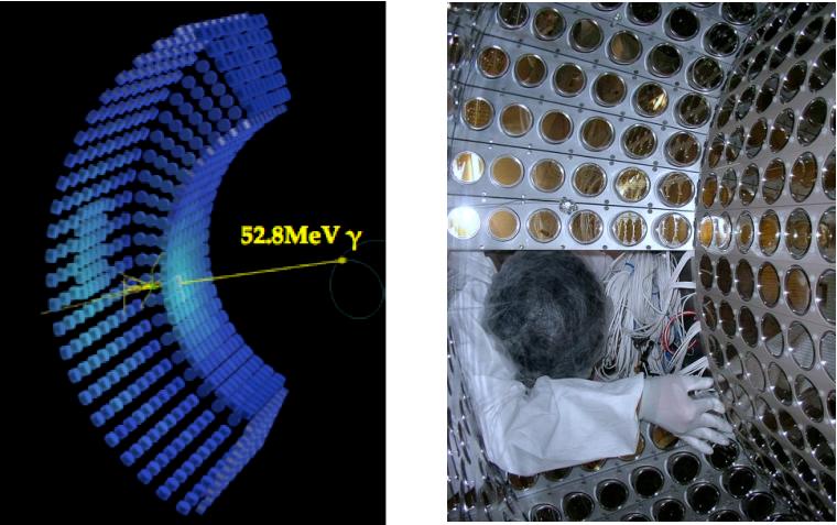
The photon entrance inner face was covered by 216 PMTs with a minimum spacing between adjacent PMTs. The photo-cathode of the PMT was, however, round-shaped with a diameter of which was much smaller than the interval between adjacent PMTs of . The performance of the MEG LXe photon detector was limited due to this non-uniform PMT coverage. Figure 56 shows the efficiency of scintillation light collection as a function of the depth of the first interaction for signal photons of . The collection efficiency strongly depended on the incident position. The non-uniform response was partly corrected for in the offline analysis, but it still deteriorated the energy and position resolutions due to event-by-event fluctuations of the shower shape, especially for shallow events.


The main concept of the upgrade of the LXe photon detector for MEG II is to reduce this non-uniform response
by replacing the PMTs on the inner face with smaller photo-sensors.
Figure 57 shows a comparison of how the same event would look for
the two cases with the current PMTs and smaller photo-sensors ()
on the inner face.
The imaging power is greatly improved with smaller photo-sensors.
For example, two local energy deposits in the same shower are clearly separated in this event.
It turns out that both the energy and position resolutions greatly improve
especially for shallow events as shown in Sect. 6.6.
SiPMs are adopted as smaller photo-sensors for the inner face of the MEG II LXe photon detector.
The motivation for choosing SiPM is discussed in detail in Sect. 6.2.
The PMTs which were used on the inner face of the MEG LXe photon detector are re-used on the other faces.
It turns out by detailed MC studies that the best use of those PMTs
is achieved by modifying the layout of the PMTs on the lateral faces.
Figure 58 illustrates the modified layout viewed on a - section.
The inner face extends along , outside the acceptance region by 10% on each side.
The extended volume reduces the energy leakage for events near the lateral walls.
The PMTs on the lateral faces are tilted such that all the photo-cathodes lie in the same plane.
This configuration minimises the effect due to shower fluctuations for events near the lateral walls.
The energy resolution is thus improved especially for those events.

6.2 Development of VUV-sensitive MPPC
6.2.1 MPPC advantage
The MPPC® (Multi-Pixel Photon Counter), a new type of photon counting device produced by Hamamatsu Photonics K.K., is a kind of SiPM device. The MPPC has many excellent features suited for the MEG II experiment. It is insensitive to magnetic fields and is sensitive to single photons, which enables an easier and more reliable calibration of the detector. Moreover, a finer read-out granularity of the scintillation light with MPPCs allows for a more precise reconstruction of shallow events. Less material budget before the LXe active region results in a 9% higher detection efficiency, as discussed in Sect. 6.6. The typical bias voltage is less than .
6.2.2 Issues
There are several issues to be addressed concerning the detection of LXe scintillation light by MPPCs.
The first issue is the photon detection efficiency (PDE) for VUV light. There are two types of layer structures for the SiPM, p-silicon on an n-substrate (p-on-n) and n-on-p. In general, since the ionisation coefficient for electrons is higher than that for holes, the breakdown initiation probability of electrons is always higher than that of holes. Blue light is absorbed close to the SiPM surface and electrons initiate the avalanche breakdown in the p-on-n case, which results in a higher sensitivity in the blue light region. Our MPPC uses the p-on-n structure, which is suitable to detect the blue light. The PDE of standard MPPC for VUV light is, however, nearly zero since VUV photons can not reach the sensitive layer due to a protection coating layer made of epoxy resin or silicon rubber. Furthermore, an anti-reflection (AR) coating layer is not optimised to the refractive index of LXe at the scintillation light wavelength.
The second issue is the MPPC size. The current largest single MPPC commercially available is , which is still too small to cover the inner face of the LXe photon detector with an affordable number of read-out channels. It is desirable to develop a large-area MPPC with or larger. However, the larger size of MPPCs could cause a larger dark count rate, larger gain non-uniformity, and larger capacitance (longer tail in the waveform, larger noise etc.) [130].
A large-area UV-sensitive MPPC has been developed in collaboration with Hamamatsu Photonics to be used in the upgraded LXe photon detector. We will describe its characteristics in the following sections.
6.2.3 PDE
Many prototypes optimised for VUV detection have been produced by Hamamatsu Photonics, which have no protection coating, a thinner contact layer or optimised AR coating with different parameters.

We succeeded in detecting the LXe scintillation light from -events by using one such prototype sample. Figure 59 shows signal waveforms from the MPPC sample (upper figure) and a UV-sensitive PMT (lower one) for the same event.
The number of detected photoelectrons for -event is calculated from the ratio of the observed charge to that obtained for a single photoelectron event. The PDE is then estimated from a ratio of the detected number of photoelectrons to the expected number of incoming scintillation photons from -events. This PDE still contains contributions from cross-talk, after-pulses, and the infrared component of the LXe scintillation light. The contribution from the infrared component is estimated to be 1% indirectly, by using the signal observed with a commercial MPPC (S10362-33-100C), which is supposed to be insensitive to the VUV component. The cross-talk + after-pulse components are estimated using a flashing LED in such a way that the MPPC detects less than 1 p.e. on average. The expected 1 p.e. probability () is calculated from the Poisson distribution with the mean estimated from the observed probability of 0 p.e. events. We can estimate the cross-talk+after-pulse probability by comparing this with the measured probability of 1 p.e. events ()[131]. This method yields a cross-talk + after-pulse probability = . of between %, depending on the over-voltage.
Figure 60 shows the measured PDEs for four MPPC samples after correcting for the contributions from cross-talk and after-pulses. There is roughly a 30% uncertainty in the PDE value, that is estimated from the variation of the PDE measured in different setups. The result shows that the PDE is higher than the 15% PDE measured in LXe, which is similar to the QE for the UV-sensitive PMT of the current detector (16%). Since the sensor coverage on the inner face is increased by 50% using MPPCs, the total photoelectron statistics would be increased.
6.2.4 Temperature dependence
Thermally generated free carriers in a depleted layer produce dark counts. The typical dark count rate is at room temperature. The dark count rate is known to be suppressed by five orders of magnitude at LXe temperature () [132]. Our test measurements confirm that the dark count rate is reduced down to for samples at LXe temperature as shown in Fig.61.

Poly-silicon was used in the previous versions of MPPCs as quenching resistors, but now switched to metal resistors are more common.
However, the resistivity of the poly-silicon increases when the temperature decreases, for example, the resistance at LXe temperature is measured to be more than a factor of two higher than at room temperature. A metal quenching resistor, which has 1/5 of the temperature coefficient of a poly-silicon resistor, is more suitable in our application in order to keep the quenching resistance low, which can avoid long fall time of MPPC signal.
The breakdown voltage of MPPCs is known to have a relatively large temperature coefficient () and the gain and PDE can, therefore, easily shift depending on the temperature, influencing the stability of the detector performances.
The LXe temperature stability of the MEG LXe photon detector has been measured to be smaller than (RMS), most likely dominated by the precision of the temperature measuring device. The fluctuation of the MPPC gain at an over voltage around is expected to be smaller than 0.1% (RMS). The PDE at around over voltage is already saturated, and no fluctuations are expected from temperature variation. The voltage dependence of the cross-talk and the after-pulse of the MPPC should be smaller than 30%/V, which corresponds to 0.23%. These fluctuations are smaller than the expected energy resolution of the MEG II LXe photon detector described in Sect. 6.6.
6.2.5 Radiation hardness
Radiation produces defects in the silicon bulk or at the Si/SiO2 interface of SiPMs. As a result, some parameters of SiPMs such as the breakdown voltage, leakage current, dark count rate, gain, and PDE may change after irradiation. There have been many studies on the radiation hardness of SiPMs irradiated by photons, neutrons, protons, or electrons. These studies show the following.
An increased dark count rate was observed at more than , and loss of single p.e. detection capability was observed at more than [133]. From the neutron flux measured in the MEG experimental area, the total neutron fluence is estimated to be less than in MEG II.
Increased leakage current was observed with a photon irradiation of [134], while the photon dose in the MEG II is estimated to be .
The radiation damage by photons, or neutrons should not be an issue for the MPPCs in MEG II.
6.2.6 Linearity
SiPMs show a non-linear response when the number of incident photons is comparable to or larger than the number of pixels of the device. The optimal condition is that the number of incident photons be much smaller than the number of pixels without any localisation. Figure 62 (top) shows the measured response functions for SiPMs with different total numbers of pixels illuminated by a laser pulse [135]. For the MEG II LXe detector, the expected number of photoelectrons reaches up to p.e. on sensor area for very shallow signal events as shown in Fig 62 (Bottom), which is only 20% of the total number of pixels, . Considering also that some of the fired pixels are recovered during the emission time of the scintillation light, the expected non-linearity is, therefore, small and can be corrected for by a careful calibration.


6.2.7 Large area MPPC
The current largest MPPC () is still too small for the MEG II LXe photon detector, and we need at least to replace the PMTs. For a larger size sensor, we have to pay attention to a possible increase in the dark count rate, an increase of the sensor capacitance, and gain non-uniformity over the sensor area.
The increase of the dark count rate is not an issue in MEG II due to the LXe temperature. To reduce the sensor capacitance, the large area of is formed by connecting in series four smaller MPPCs () each). In this configuration, the decay constant of the signal waveform becomes from . To equalise the gain in the large area sensor, four MPPCs are selected with similar breakdown voltages.
Instead of a simple series connection, each sensor chip is decoupled with a capacitor to enable the bias voltage to be supplied via a parallel connection. In this way, we can still extract signals from the series connection, and the common bias voltage such as can be supplied to the four sensor chips.
6.3 Detector design
6.3.1 Design of sensor package and assembly
Figure 63 shows a design of the UV-enhanced MPPC package used for the MEG II LXe photon detector. Four sensor chips with a total active area of are glued on a ceramic base of . The ceramic is chosen as a base material because the thermal expansion rate is close to that of silicon at LXe temperatures.

The sensor active area is covered with a thin high quality VUV-transparent quartz window for protection. The window is not hermetic; there is a gap between the sensor and the window in which LXe penetrates. Figure 64 shows the transmission efficiency of different window materials as a function of wavelength [136], showing that the transmittance of the synthetic silica, which is used in our MPPC, is quite high for the LXe scintillation light (). The reflection loss is small since both sides of the quartz window touch LXe whose refractive index is close to that of the quartz window (, ).
The MPPCs are mounted on a PCB strip as shown in Fig. 65. Each PCB strip has 22 MPPCs, and two PCBs are mounted in a line along the -direction with 93 lines (186 strips) covering the -direction on the inner wall of the detector cryostat as shown in Fig. 66. The total number of MPPCs is 4092. One MPPC package has eight electrode pins (an anode and a cathode from each sensor chips) which are plugged into the corresponding sockets on the PCB. This mounting scheme allows easy replacement of the MPPC module if necessary. The PCB has additional circuit parts of capacitances and resistors to realise the signal line in series and the bias line via parallel connection as described in Sect. 6.2.7.


The signals from the MPPCs are transmitted on the signal lines of the PCB which are designed to be well shielded from both outside and the adjacent channels and have a impedance. Similar PCBs are used in the feed-throughs of the cryostat as described in Sect. 6.3.3.
It is important to precisely align the PCB strips on the inner wall of the detector cryostat and to minimise the gap between the strips and the wall since LXe in this gap deteriorates the photon detection efficiency and causes an undesirable low energy tail in the energy response function of the detector. Figure 67 shows the inside of the LXe photon detector after the MPPCs and PMTs are mounted.

6.3.2 Design of PMT support structures
Figure 68 shows the 3D CAD design of the PMT support structure. There is no support structure at the inner side, and only the outer part has screw holes to an arch-shaped support structure repaired by bolts. Joint brackets are used to fix two adjacent side slabs. The side and outer faces of the PMT support structure are re-used from the MEG LXe photon detector, while the top and bottom panels are modified to fit the larger number of PMTs, 73 instead of 54. In total, 668 PMTs are installed in five faces except for the inner one.

6.3.3 Signal transmission
The transmission of 4092 MPPC signals to the DAQ electronics without introducing noise or distortion is challenging. We have to pay attention to pickup noise, cross-talk, and limited space in the cryostat as well as the feed-throughs etc. In order to overcome such issues, we have developed a multi-layer PCB with coaxial-like signal line structure. It is used for both the PCBs for MPPC mounting and the vacuum feed-through of the cryostat.

As described in Sect. 6.3.1, 22 MPPCs are mounted on a PCB strip and signal lines embedded in the strip transmit signals to an end. The total length of the signal lines is about , and the width of the PCB is . MPPCs are plugged into socket pins on the PCB and 22 MMCX (micro-miniature coaxial) connectors are used at the end of the signal lines. The signal lines on the PCB strip are connected to (real) thin coaxial cables by means of connectors at the edge of PCBs. Then the signals are transmitted to feed-throughs using the thin coaxial cables, with a length of depending on their positions. The coaxial cables (RG178-FEP) are produced by JYEBAO[137]. An MMCX connector is assembled on one end, and the other end is directly soldered on the feed-through PCB.

Figure 69 shows the layer structure of the PCB used as our feed-through PCB. Each signal line is surrounded by different ground patterns to minimise cross-talk and to shield from the outside. To avoid any ground loop, different ground patterns for different signal lines are separated. In total, six layers (two layers of signal, and four layers of ground) are used. The dimensions of the layers are adjusted to have a impedance. The MEG LXe photon detector had in total 10 DN160CF flanges for the signal and HV cables of 846 PMTs. Since the number of readout channels has increased, more feed-through ports are necessary. A PCB-type feed-through shown in Fig. 70 similar to the PCB for MPPC mounting has been developed, which allows a high density signal transmission through vacuum walls and a low-noise environment. On both sides of a PCB, 72 cables are directly soldered, and six PCBs are glued by Stycast 2850 FT + Catalyst 24 LV into a DN160CF flange. In total, 10 DN160 CF flanges are used for MPPC signals (up to 4320 channels) and 2 flanges for PMT signals, while 4 flanges are used for PMT HV cables. The signal from the feed-through is transmitted to the readout electronics via 10 m coaxial cables.
6.3.4 Read-out electronics
Both the PMTs and MPPCs signals are read out by WaveDREAM boards (WDBs). Amplifiers are mounted on the boards with switchable gain settings from 0.5 to 100 (see Sect. 8.2 in detail). The different gain stages can then be switched at any time. The higher gain mode is used to detect single photo-electrons for the calibration of the MPPCs, while the low gain mode is used to take physics data where a large dynamic range is needed.
No amplifier is installed between MPPC and WDB. The bias voltage for MPPC, which is typically , is supplied from the WDBs through the signal cable.
6.3.5 Cryogenics
The MEG LXe cryostat is re-used for the MEG II LXe photon detector. In order to cover the increase of the external heat inflow due to extra signal cables for the MPPCs, the cooling power of the refrigerator is increased by adding another Gifford-McMahon (GM) refrigerator, model AL300 produced by CRYOMECH [138]. The new refrigerator will produce more than of cooling power which should be sufficient to cool the MEG II LXe photon detector.
6.4 Calibration and monitoring
The LXe detector necessitates careful calibration and monitoring of the energy scale over its full energy range. That requires several methods that have already been introduced and commissioned in MEG and will be inherited by MEG II with some modifications to match the upgrade. They are listed in Table 6 and summarised in the following (see [1] for more details):
- 1.
The behaviour of the LXe photon detector is checked in the low-energy region using -rays from an AmBe source, placed in front of the inner face, and -particles from 241Am sources deposited on thin wires, mounted inside the active volume of the detector. The -signals are also used to evaluate and monitor in-situ the PMT quantum efficiencies (QEs) and measure the Xe optical properties on a daily basis. In addition, -rays from capture by 58Ni of thermalised neutrons produced by a neutron generator are also available. This is the only method which allows to check the response of the LXe photon detector with and without the particle flux associated with the muon beam and/or the other beams.
- 2.
The performance of the LXe photon detector in the intermediate-energy region is measured two/three times per week using a Cockcroft–Walton accelerator, by accelerating protons, in the energy range , onto a Li2B4O7 target. -rays of energy from are used to monitor the energy scale, resolution and the uniformity of the detector, while time-coincident 4.4 and -rays from are used to inter-calibrate the relative timing of the LXe photon detector with the pTC detector.
- 3.
The response of the LXe photon detector around the signal region and above is measured once/twice a year using photons from decays produced by the charge exchange reaction (CEX) in a liquid hydrogen target, . Photons with energy of are also produced via the radiative capture reaction, , with a relative probability of [139] (Panofsky ratio).
- 4.
The RMD can be used as well for calibration purposes with dedicated triggers. In particular the selection of the pair represents a strong quality check of the complete apparatus and a straightforward way to extract the global time resolution (the resolution of the timing difference between the positron and the photon) and the relative offset.
| Process | Energy | Main Purpose | Frequency | |
|---|---|---|---|---|
| Cosmic rays | from atmospheric showers | Wide spectrum (GeV) | LXe–CDCH relative position | Annually |
| LXe purity | On demand | |||
| Charge exchange | MeV photons | LXe energy scale/resolution | Annually | |
| Radiative decay | Photons , | LXe–pTC relative timing | Continuously | |
| Positrons | ||||
| Proton accelerator | 14.8, 17.6 MeV photons | LXe uniformity/purity | Weekly | |
| 4.4, 11.6, 16.1 MeV photons | LXe–pTC timing | Weekly | ||
| Neutron generator | 9 MeV photons | LXe energy scale | Weekly | |
| Radioactive source | 5.5 MeV ’s | LXe PMT/SiPM calibration | Weekly | |
| LXe purity | ||||
| Radioactive source | 4.4 MeV photons | LXe energy scale | On demand | |
| Radioactive source | 136 (11 ), 122 keV (86 ) X-rays | LXe–spectrometer alignment | Annually | |
| LED | UV region | LXe PMT/SiPM calibration | Continuously |
6.5 Alignment
Precise relative alignment of the photon detector and the positron magnetic spectrometer is important to ensure that the angular acceptance criteria for signal events are not compromised. For example, a error in the measured position of the photon in the LXe photon detector would result in a signal event possibly being missed because it would not be consistent with being emitted opposite to the direction of the positron. The relative alignment of the LXe photon detector and the spectrometer is implemented using optical survey techniques. For the LXe photon detector, the survey is complicated by the fact that the photo-sensors (SiPMs) are not visible once the LXe photon detector is closed and that their positions relative to the external survey markers change due to thermal contraction and buoyant forces as the LXe photon detector is cooled and filled with liquid xenon.
6.5.1 The X-ray alignment system for the LXe photon detector
A newly introduced technique will measure the position of each SiPM using the novel technique of X-ray imaging each sensor. The technique uses a well collimated and precisely aligned X-ray beam in the radial direction originating from the axis of the COBRA magnet (at in the MEG coordinate system) at precisely known axial () and azimuthal () coordinates. The X-rays are collimated to produce a ribbon-like beam, narrow (% of the dimension of a SiPM at its face) in one dimension ( or ). The energy of the X-rays is chosen such that they penetrate the COBRA and LXe cryostats with significant probability, yet interact within of liquid xenon, primarily by photo-absorption. Scintillation light produced by the photo-electrons in the liquid xenon is detected by the SiPM directly in front of the interaction. The -coordinate of each SiPM is deduced by orienting the narrow () beam dimension in the axial direction and then scanning it in that direction. The axial extent of a given SiPM is given by the axial extent of the X-ray beam position for which light is detected in that element. The -coordinate is similarly determined by rotating the collimator so the beam is narrow in the azimuthal direction and scanning in azimuth.
The X-rays are produced by decay of a source, producing X-ray lines at (%) and (%). They penetrate the COBRA magnet and the front of the LXe cryostat with % probability. We use a commercial point source with an activity of and collimate the beam to with a brass collimator. The -coordinate of the origin of the beam and its -direction are set using precise linear and rotary translation stages. The signal induced in the SiPM is about 30% of that induced in a single SiPM by a typical shower of a photon from events. Data are collected by implementing a trigger on the signal detected in a limited number of SiPMs in the region to which the X-ray beam points.
The expected performances is studied with a Geant4 MC simulation of the X-ray beam and the MEG II detector. X-rays are generated in the beam solid angle, propagated through the COBRA cryostat and into the LXe. Scintillation light is produced from the electron produced by the X-ray interaction and the SiPM response is simulated. Figure 72 shows a plot of the average number of detected photoelectrons per interaction in a SiPM as a function of the difference between the -coordinate of the beam with respect to the -coordinate of the SiPM centre. Each bin contains detected X-rays, corresponding to an exposure time of per position. An approximate estimation of the precision with which the SiPM centre -coordinate can be measured is obtained by fitting the distribution with a Gaussian; the statistical uncertainty is . Similar precision is obtained fitting the distribution with a rectangular function smeared with error functions.
Systematic uncertainties in the position determination will be due to the uncertainty in our knowledge of the direction and origin of the X-ray beam. The position and angle alignment of the collimator is made by an optical survey to a precision of and . Variations in the beam direction as it moves along the translation stage (of the order of from the device specifications and our measurements) will be monitored with a laser attached to the translation stage and projected to a quadrant photodiode, as well as with a spirit-level on the translation stage. In addition, a cross-check of the optical survey of the cryostat and the X-ray beam is made by mounting small LYSO1515 15 Lutetium-yttrium oxyorthosilicate Lu2(1-x)Y2xSiO5. crystals scintillators and thin lead absorbers in well-surveyed positions just in front of the LXe cryostat. The X-ray beam should be detected in the LYSO detectors at the calculated X-ray beam - and -coordinates and the signal in the LXe should be shadowed at the calculated X-ray beam - and -coordinates of the thin lead absorbers.

6.6 Expected performance
The expected performance of the upgraded LXe photon detector is evaluated using a MC simulation.
6.6.1 Simulation
A full MC simulation code based on Geant4 was developed to compare the performance of the MEG and the MEG II design. In the simulation, scintillation photon propagation is simulated by Geant4. The reflection of scintillation photons on the MPPC surface was simulated using the complex refractive index of a pure silicon crystal. The reflectance is typically about 60%. In the simulation, the index-number of hit pixel and the arrival time of each scintillation photon are recorded. They are used to form avalanche distributions in each MPPC. The dark-noise, optical cross-talk, after-pulsing, saturation and recover are modelled based on real measurements and incorporated in the simulation. The waveform of the MPPC is simulated by convolving the single photo-electron pulse and the time distribution of avalanches. A simulated random electronics noise is added assuming the same noise level as the MEG read-out electronics.
The event reconstruction analyses are basically the same as those for the MEG detector, while the parameters, such as waveform integration window and corrections for light collection efficiency depending on the conversion position, are optimised for the new design. The non-linear response of the MPPC due to pixel saturation (see Fig. 62), resulting in a non-linear energy response of the detector, is taken into account. However the effect on the energy reconstruction is negligible because the fraction of the total number of photoelectrons observed by each MPPC is small.
6.6.2 Results
Figure 71 shows the position resolutions for signal photons as a function of the reconstructed conversion depth (). In MEG, the position resolution is worse in the shallow depth part than in the deeper part because of the PMT size. The position resolution in the shallow part is much better in MEG II due to smaller size of the photo-sensors.
The energy resolution is also much better in the shallow part with the MEG II design than that of MEG as shown from the probability density function (PDF) for photons in Fig. 73 due mainly to a more uniform photon collection efficiency. The low energy tail is smaller because of the lower energy leakage at the acceptance edge with the improved layout of the lateral PMTs. The resolution is also better in the deeper part because of the modification of the angle of the lateral PMTs.
The measured energy resolution of MEG (1.7% for ) was worse than that in the simulation (1.0% for ). The reason is not fully understood, while the source of the difference could be related to the behaviour of the PMTs (e.g. gain stability, angular dependence and so on) or the optical properties of liquid xenon (e.g. effect of convection). In the former case, the difference can become smaller in the upgraded configuration. On the other hand, in the latter case, the difference could remain. Figure 74 shows the energy response under different assumptions:
- 1.
the additional fluctuation completely vanish in MEG II,
- 2.
a part of fluctuation remains which corresponds to 1.2% resolution in MEG (the resolution achieved with the MEG LXe large prototype detector),
- 3.
the fluctuation remains making the resolution of MEG 1.7%.
We will use the assumption 2 for the sensitivity calculation in Sect. 9.
The time resolution of the LXe photon detector can be separated into six components; the transit time spread (TTS) of the photo-sensors, the statistical fluctuation of scintillation photons, the timing jitter of the read-out electronics, the electronics noise, the resolution of the photon conversion point and the finite size and the fluctuation of the energy deposits in the LXe. Most of these are common to both MEG and MEG II, but the effect from the TTS and electronics noise are different because of the different photo-sensors. The effect of the TTS is negligible because it scales as a function of the number of photoelectrons, and the light output of liquid xenon is large. The effect of the electronics is larger in MEG II than in MEG because the leading time of an MPPC pulse for liquid xenon scintillation signal is slower than that of a PMT pulse. In order to estimate the effect, the time resolution of the upgraded detector for signal photons is measured in the simulation. The evaluated time resolution with preliminary waveform and reconstruction algorithms is assuming a noise level up to . The main improvements come from the better time of flight estimate, deriving from the better position reconstruction, and higher photon statistics. Since parameters such as the rise time of the waveform and the noise components may not be correctly considered in the simulation, the time resolution in the worse case might still be at the MEG level, hence a conservative estimation is .
6.6.3 High intensity
The higher background photon rate due to the higher muon intensity in MEG II should not be a problem for the photo-sensor operation. On the other hand, the background rate in the analysis photon energy region would be increased due to pile-up. In the MEG analysis, the energies of pile-up photons are unfolded using the waveform and light distribution on the inner face.
In 2011 we took data with the MEG LXe detector at different beam intensities: 1.0, 3.0, 3.3 and . Figure 75 shows the photon spectrum normalised to the number of events from ; the scaling factors are consistent with to the muon stopping rate on the target. The shapes of spectra are almost identical in the analysis region after subtracting the energies of pile-up photons. Since the same analysis can be used also for the MEG II upgraded detector, a higher beam rate is not expected to cause an additional background rate due to pile-up.
7 Radiative Decay Counter
The Radiative Decay Counter (RDC) is an additional detector to be installed in MEG II. It is capable of identifying a fraction of the low-energy positrons from RMD decays having photon energies close to the kinematic limit, which are the dominant source of photons for the accidental coincidence background. This section describes the concept and the design of the detector, as well as the results of the pilot run and the expected performances.

7.1 Identification of the RMD photon background
As mentioned in Sect. 1, RMD and accidental coincidences are the backgrounds in search. In the case of the accidental background, which is dominant in MEG II, photons are produced from either RMD or positron AIF. Figure 76 shows the fraction of background photons expected in MEG and MEG II from different sources. The AIF background decreases in MEG II thanks to the reduced mass of the CDHC compared with the MEG drift chambers and it is possible to decrease it further by looking for a disappearing positron track in the analysis. On the other hand, the RMD photon background does not change. Therefore, it is important to identify these events. According to simulations, the RDC can detect % of the RMD photon background events (), (the product of the fraction of positrons going downstream (%) and the RDC positron detection efficiency (%, see Table 7)) thus improving the sensitivity of the search by 15%.
The RDC will be installed downstream the stopping target as shown in Fig. 77. A fraction of the RMD events can be identified by tagging a low-energy positron in time coincidence with the detection of a high energy photon in the LXe detector. This low-energy positron of (with ) follows an almost helical trajectory with small radius around the B-field lines. Therefore, it can be seen by a small detector with a radius of only , placed on the beam axis. There is an option to install a detector also upstream, as described in Sect. 7.6.

7.2 Detector design
The red histogram in Fig. 78 shows the expected distribution of the time difference between RDC and the LXe photon detector for accidental background events (with photons from RMD or AIF), while the blue histogram is the distribution due to signal events. The peak in the red histogram corresponds to the RMD events, while the flat region in both histograms corresponds to background Michel positrons. As the detector is placed on the beam-axis, there are many background Michel positrons (). They can be distinguished from RMD positrons by measuring their energy since they typically have higher energies as shown in Fig. 79. Hence, the RDC consists of fast plastic scintillator bars (PS) for timing and a LYSO crystal calorimeter for energy measurements.


Figure 80 shows a schematic view of the RDC detector: 12 plastic scintillator bars in the front detect the timing of the positrons, and 76 LYSO crystals behind are the calorimeter for energy measurement. In order to distinguish RMD positrons from Michel ones, both the PS and the LYSO calorimeter are finely segmented. Because the background rate is larger close to the beam axis, the width of the PS in the central region is while it is at the outer part. The size of each LYSO crystal is .

The PS shown in Fig. 81 consists of plastic scintillators read out by SiPMs. The design of the PS is very similar to that of the pTC (Sect. 5). In order to have good timing resolution, scintillators must have a high light yield and short rise time. BC-418 from Saint-Gobain [116] was selected as it satisfies these requirements. The scintillation light is read out by SiPMs at both ends of each scintillator. SiPMs are compact and operate in high magnetic fields, and so are suitable for the RDC having many readout channels in a limited space. The MPPC S13360-3050PE from Hamamatsu Photonics [140] was selected for the SiPM for PS because of its high gain and high photon detection efficiency. In order to detect as much scintillation light as possible, multiple SiPMs (two for the central part and three for the outer part) are attached to both ends of the scintillators. The SiPMs are connected in series on the readout printed circuit boards (PCBs) to reduce the number of readout channels and to reduce the rise time of the signal due to the reduced capacitance. They are glued to the scintillators by optical cement. Each scintillator is wrapped with a thick reflective sheet (ESR from 3M) to increase light yield and to provide optical separation as well as black sheets of Tedlar for light shielding.

The calorimeter is made of 76 LYSO crystals (Shanghai Institute of Ceramics). LYSO crystals have a high light yield () and a short decay time constant (). These characteristics are suitable for the measurement of positron energy in a high rate environment. LYSO contains the radio isotope 176Lu, which decays to 176Hf with emission of a (with end-point energy of and half life of ), followed by a cascade of -rays. As described in Sect. 7.4, this intrinsic radioactivity can be used for an energy calibration. The decay rate is measured to be small (), therefore not affecting the detection of positron from RMD. Each LYSO crystal is connected to one SiPM at the downstream side (see Fig. 82). A SiPM with a small pixel size of (S12572-025 from Hamamatsu Photonics [141]) was selected as it has good linearity for high intensity of incident scintillation light. The SiPM has spring-loaded contact to the crystal, using optical grease, instead of being glued. Therefore, it is possible to replace the SiPM or the crystal.

7.3 Tests and construction in the laboratory
The characteristics of each SiPM for the PS are measured before construction. The breakdown voltage is obtained for each SiPM from the measurement of the current–voltage response curve. SiPMs with the breakdown voltages close to each other are grouped together and connected in series. After the construction of the PS, the timing resolution of each counter is measured to be less than by using a 90Sr source.
The LYSO crystals are also tested individually. We measured the light yield and the energy resolution of all the crystals by using a 60Co source. The energy resolution was measured to be % at for all the crystals. In a high rate environment, energy resolution can be worsened by the “afterglow” effect of LYSO. Afterglow is a delayed light emission of crystals with very long time constant (typically few hours). This effect was studied by exposing the crystals to a 90Sr source. The increase of the current due to afterglow was measured with the SiPMs attached to the crystals. According to this measurement, the expected increase of the current in the MEG II beam environment is estimated to be at maximum. The influence on the energy resolution is expected to be less than 1% at .
The support structures of the PS and of the LYSO calorimeter are constructed with non-magnetic materials such as aluminium. The front part of the PS is not covered with metal, in order to minimise the amount of material. In order to absorb the stress of the springs ( in total) with the minimum amount of material, a Rohacell plate sandwiched with two CFRP (Carbon Fibre Reinforced Polymer) plates ( each) is inserted between the PS and the LYSO calorimeter. In addition, a thin aluminium plate is inserted for better light shielding. The back side of the crystals is covered by two Delrin® plates and one CFRP plate.
Figure 83 shows the RDC mounted on a moving arm system attached to the end-cap of the COBRA magnet. The RDC can be remotely moved away from the beam-axis when the calibration target for the LXe photon detector is inserted from the downstream side. The moving arm is controlled by water pistons made of plastic, which work in a magnetic field. The supporting mechanics are made of aluminium except for the titanium shaft, which works under heavy loads. The end-cap of COBRA separates the inner volume (filled with helium) from the outside. SiPM signals are transmitted through the end-cap by using feed-through PCBs attached to the end-cap. The design of the feed-through is essentially the same as used for the LXe photon detector (see Sect. 6.3.3).

7.4 Pilot run with a muon beam
The full detector system was tested in the E5 beam line at PSI with a beam intensity of . The RDC was mounted at the downstream end of the COBRA magnet. For the detection of photons from RMD, a BGO detector consisting of 16 crystals ( each) was used as a substitute of the LXe photon detector. RMD events were acquired by requiring an energy deposit larger than in the the BGO. After event selection to reject cosmic rays, events remained. The distribution of the time difference between the BGO hit and the PS hit is shown in Fig. 84. A clear peak corresponding to RMD events is successfully observed.

Figure 85 shows the measured distribution of the energy loss in the LYSO calorimeter. Higher energy tail events are mainly Michel positron backgrounds, while the low energy part () corresponds to RMD. For a demonstration, we applied an event selection to reject events with an energy release in the calorimeter above . The red histogram in Fig. 84 shows the timing distribution after the calorimeter LYSO energy cut. The flat region which corresponds to backgrounds is reduced to by this cut. The peak region (i.e. RMD events) is also reduced to because the energy threshold for the BGO trigger was low and therefore the energy of the RMD positron could be high.

7.5 Expected performance
The sensitivity of the search in MEG II including the RDC is calculated by using the expected timing difference distribution of the RDC and LXe photon detectors (see Fig. 78) and the expected energy distribution in the LYSO calorimeter (see Fig. 79) (see Sect. 9 for the details). In the MEG physics analysis [142, 143, 3], the likelihood depends on the number of events (signal and background) and the probability density functions (PDF) based on the energy, timing and relative angles of positron and photon. The RDC observables can be added in the likelihood analysis by using the PDFs of the PS–LXe timing difference and of the LYSO calorimeter energy. Table 7 summarises the performances of the RDC assumed in the calculation. By using the RDC, the sensitivity of MEG II is expected to improve by 15%.
| Parameter | Value |
|---|---|
| LYSO energy threshold | |
| RMD detection efficiency | 100% |
| LYSO energy resolution | 8% |
| Time resolution | |
| Accidental probability | 9% |
| RMD acceptance | 88% |
7.6 Further background reduction with an upstream RDC
Because half of the positrons from RMD go upstream, it is possible to further improve the sensitivity by adding an additional RDC in the beam line upstream the muon stopping target, near the end of the COBRA magnet. The upstream RDC has to be very different from the downstream RDC as it must be placed on the beam path. First of all, the material thickness must be small enough to minimise the impact on the beam which prevents the use of a calorimeter. Secondly, the detector must be able to distinguish the RMD positrons from beam muons. This could be possible with a fast response, finely segmented detector.
A possible candidate is a layer of scintillation fibres with SiPM readout. Fibres can be bundled at both ends to reduce the number of readout channels. A fibre candidate is BCF-12 (Saint-Gobain [90]), a double-clad square shaped fibre wide. With this thickness, the effect to the muon beam optics is expected to be negligibly small. However, radiation damage on fibres and pile-up of the beam muon signals (after-pulse of SiPMs increases the pile-up probability) may affect the detector performance.
Another candidate is a synthetic diamond detector. Diamond detectors have fast signal, and can be manufactured in a thin layer. They are also known to be radiation hard. The drawback is their low signals, which requires high gain amplifiers with low noise.
The estimated improvement of the sensitivity with the upstream RDC is 10% when the detection efficiency is 100%.
8 Trigger and DAQ
This section describes an innovative integrated trigger and data acquisition system designed for the MEG II detector. After a description of the main requirements, the designed circuit characteristics and their interplay are described. We conclude with the latest results from the research and development phase.
8.1 Requirements
The MEG II sensitivity goal requires a substantial detector and read-out electronics redesign to deal with a factor of two increase in muon stopping rate with respect to MEG. As a consequence we replaced many of the PMTs of the LXe and timing counter detectors with SiPMs and MPPCs; similarly the new CDCH design requires more read-out channels compared to the MEG drift chambers. In summation this has led to an almost tripling of read-out channels with respect to MEG. The requirement for an efficient offline pile-up reconstruction and rejection is the availability of full waveform information; thus the DAQ waveform digitiser has to provide state-of-the-art time and charge resolution and a sampling speed in the GSPS range.
In addition, SiPMs have a lower gain than PMTs and require electronic signal amplification. Using SiPMs in LXe prevents us from placing preamplifiers directly next to the photo-sensors because of cooling problems; it is therefore mandatory that the new electronics contains flexible amplification stages for small signals (single photo-electrons for calibration) as well as large signals (-showers).
As shown in Fig. 86, the detector signals in MEG were actively split and then sent to the dedicated VME-based trigger and DAQ systems; the limited space for the electronics in the experimental area prevents us from adopting such a scheme with the increased number of channels expected in MEG II.

8.2 The WaveDREAM Board
The new system integrates the basic trigger and DAQ (TDAQ) functionalities onto the same electronics board, the WaveDREAM board (WDB). A simplified schematics of the WDB is shown in Fig. 87.
It contains 16 channels with variable gain amplification and flexible shaping through a programmable pole-zero cancellation. Switchable gain-10 amplifiers and programmable attenuators allow an overall input gain from 0.5 to 100 in steps of two. A multiplexer can be used to send one input signal to two channels simultaneously which can be set at different gains, at the expense of only having 8 channels per board. Two DRS4 chips [144] are connected to two 8-channel ADCs, which are read out by a Field-Programmable Gate Array (FPGA). In normal operation, the DRS4 chips work in “transparent mode”, where they sample the input signals continuously at a speed up to 5 GSPS in an analogue ring buffer. At the same time, a copy of the input signal is sent to the DRS4 output, where it is digitised continuously by the ADCs at 80 MSPS with a resolution of .
The output stream of the ADCs is used in the FPGA to perform complex trigger algorithms such as a threshold cut on the sum of all input channels. Interpolation of the ADC samples via look-up tables allows time coincidence decisions with resolutions of a few nanoseconds to be made, much less than the ADC sampling speed. In case a trigger occurs, the DRS4 chip is stopped and the internal 1024-cell analogue memory is digitised through the same ADCs previously used for the trigger. With this technique, both complex triggering and high speed waveform sampling is possible on the same board.
The SiPMs of the MEG II experiment require bias voltages in the range of . Some detectors use six SiPMs in series, which requires a maximum voltage up to . This voltage can be supplied through the signal cables with capacitive de-coupling of the signal into the amplifiers as shown in Fig. 87. An ultra-low noise bias voltage generator has been designed to accommodate these needs. A Cockcroft–Walton (CW) stage (also known as Greinacher multiplier) generates a high voltage output of at a switching frequency of (see Fig. 88).

A Proportional-Integral (PI) regulator keeps the output voltage stable by comparing it through a voltage divider with a demand voltage given by a DAC. An elaborate low pass filter reduces the output ripple to below , so that it cannot be seen, even with an amplifier gain of 100, at the input of the WDB. Since SiPMs require slightly different bias voltages, a simple DAC “sitting” at the high voltage potential can add between to the output voltage on a channel-by-channel basis (see Fig. 89).
The DAC and the ADC for current measurements are placed at a high voltage ground defined by the CW generator. An isolated DC-DC converter generates, together with a low drop-out (LDO) regulator, the power supply voltage required by the DAC and the ADC. They are interfaced through a SPI bus via a digital isolator. A separate ADC measures the CW voltage through a precision voltage divider.
At a CW voltage of for example, output voltages from can be generated for each channel, which is sufficient to accommodate variations between different SiPMs. The output current is measured via shunt resistors and a ADC with differential inputs. The voltage drop across the shunt resistor is measured and converted into a current by the control software running on the soft core processor in the FPGA. The DAC is adjusted according to the voltage drop to keep the output voltage stable independent of the current, while high voltage CMOS switches (IXYS CPC7514) are used to turn off individual channels. Different CW generators have been developed for different output voltages and powers, reaching up to and . Alternatively, a single high voltage can be distributed throughout the crate backplane, reducing costs by eliminating individual CW generators for each WDB.
Using this scheme, a cost effective and highly precise bias generator has been realised. The absolute voltage accuracy (as measured with an external multimeter) is below at a maximum current of . The current measurement has a resolution of at a full range of with an accuracy of 0.1%. The high voltage bias generator is implemented as an optional piggy-back PCB placed on top of the WDB (see Fig. 90), so it can be omitted for channels which do not need biasing (such as PMT channels which have a separate high voltage supply), thus reducing costs.

The WDB can be used in stand-alone mode, where it is read out through Gigabit Ethernet and powered through Power-over-Ethernet (PoE+). For MEG II, it has been decided to house 16 boards in a compact crate. This crate requires links for the simultaneous read-out of waveform and trigger data, a common high voltage for the SiPM biasing, an integrated trigger distribution and an ultra-low jitter clock with a few picoseconds precision. Since such a crate is not available on the market, a new standard has been developed. The WaveDAQ crate is a 3 HE 19” crate with 16+2 slots and a custom backplane as can be seen in Fig. 91. The Crate Management Board (CMB) contains the 220 V power supply together with a shelf management unit and is placed to the right side of the crate. The power supply generates a crate power of and a standby power for the shelf manager. Cooling is achieved by fans on the rear-side blowing air from the back to the front, where it exits through holes in the various boards. This topology allows stacking of crates directly on top of each other, making the whole system very compact.

The CMB contains an micro-controller programmed in the C-language. It is connected to a dedicated Ethernet network for remote control and monitoring, and has a LED display and buttons for local control. Current and temperature sensors reflect the state of the crate, and each of the 18 slots can be powered on and off individually. The micro-controller is connected to all slots via a Serial Peripheral Interface (SPI) bus. This allows detection of individual boards in each slot, communication with all WDBs as well as remote firmware updates through the backplane. A physical select line for each slot allows geographic addressing as in the “good old CAMAC days”.
The WaveDAQ crate contains 16 slots for WDBs, which provide 256 input channels. The flexibility of the WDBs allows the readout of SiPMs, PMTs and drift chamber channels. The MEG II experiment will use a total of 37 such crates for the data acquisition of all detectors. The global trigger as well as the trigger and clock distribution is also housed in WaveDAQ crates, increasing the total number to 39.
In addition, the WaveDAQ crate contains two slots for so-called “concentrator” boards. The Trigger Concentrator Board (TCB) receives 8 serial links from each WDB and is described later. The Data Concentrator Board (DCB) received two separate serial links from each WDB for waveform readout. The dual star topology allows the operation of both the trigger and the DAQ system simultaneously without interference.
An integrated trigger bus allows the distribution of trigger signals through the backplane. Busy signals from each slot are connected via a “wired-or” and are used to re-arm the trigger after an event. A low jitter clock with skew corrected PCB traces is distributed through the backplane. Measurements show a slot-to-slot variation below and a jitter below . All backplane communication signals except the busy line use the LVDS standard.
Each WDB supports hot-swap functionality. During hot insertion, an inrush current controller ramps up the board’s capacitors gently, avoiding connector sparks and backplane power supply glitches. A switch at the handle latch switches off the internal power before the board is extracted.
8.3 Data read-out: the Data Concentrator Board
The DCB is responsible for the configuration of all boards inside the crate through the SPI links, the distribution of the master clock and trigger signals, the readout of waveform data from each slot through dedicated serial links, the merging and formatting of the data, and the interface to the global DAQ computers through Gigabit Ethernet. It uses a Xilinx Zynq-7030 chip which contains a dual-core ARM Cortex-A9 processor embedded in the FPGA fabric and running at . This chip is complemented with a SD card to store the Linux operating system, of DDR3 RAM, and a Small Form-Factor Pluggable (SFP) transceiver for 1 or Ethernet. A dedicated clock distributor with integrated jitter cleaner (LMK03000 [145]) receives an internal or external clock and distributes it through the backplane to all slots via a star topology.
A dedicated font-end program runs on the ARM processors which collects waveform data from all 16 WDBs, merges them into one event, and sends it to the central DAQ computers via Gigabit Ethernet (optional ). The event format is compatible to the MIDAS DAQ system used in MEG II. In addition, the front-end program configures and monitors all WDBs and the TCB through the SPI links. It can communicate to the CMB to reboot individual slots in case of problems or firmware upgrades.
8.4 Trigger processing: Trigger Concentrator Board
The trigger processing includes suppressing the background by almost six orders of magnitude resulting in an acquisition rate of about . The real time reconstruction algorithms rely on the fast response detectors: the LXe detector for the photon observables and the pTC for the positron ones. The ionisation drift time in the CDCH cells prevents the trigger system from using any information from the track reconstruction from trigger level 0.
Event selection relies on an on-line reconstruction of decay product observables, such as momenta, relative timing, and direction. Logic equations are mapped in FPGA cells and implemented at 80 MHz so as to be synchronous with the FADC data flow. An estimate of the photon energy is obtained by the linear sum of pedestal-subtracted signal amplitudes of LXe photo-sensors, each weighted according to their own gain, which is efficiently implemented by using digital signal processor (DSP) units in the FPGA. An increased ADC resolution (12 vs. ) coupled with the improved single photoelectron response of the new sensors will allow to achieve a resolution better than that of MEG (7% FWHM at the signal energy ), though the final resolution will depend on running conditions. Concerning the relative timing, this will benefit from using WDB comparators coupled to each input signal (on both the LXe detector and pTC), whose latch time can be further refined by implementing look-up tables on the FPGA to correct for time-walk effects. Also in this case we expect the resolution to be significantly improved from the achieved in MEG; some results of the expected online time resolutions are reported in Sect. 8.7. Moreover, the enhanced imaging capability due to the finer detector segmentation (smaller LXe photo-sensors and pTC counters) permits tighter angular constraints on the decay kinematics.
The boards designed for the online data processing are called Trigger Concentrator Boards (TCB). A TCB gathers the information from a lower level trigger board, which could be a WDB via back-plane connections or another TCB which could be in another or in the same crate. In the first case the connection is provided via the back-plane in the second by a cable connected on the front panel. In order to minimise design and production costs, we decided to use the same 12-layer layout for all TCBs, independent of the role each one plays in the trigger hierarchy. TCBs differ from each other by the firmware operating on an on-board Xilinx Kintex7 FPGA [146]. Apart from reconstruction algorithms, which depend on individual sub-detectors, other features might depend on the slot assignment. For instance, the direction of I/O data lines is set from the back-plane to the FPGA if the TCB is located at the centre of the crate (Master position in all the crates), while it is the other way round for higher level TCBs hosted in a Slave position in the trigger crate, the two configuration are shown in Fig. 92.

8.5 System synchronisation: Ancillary board
The main task of the Ancillary system is to provide the TDAQ boards with an ultra-low jitter clock signal to be used as the experiment time reference. We selected a low jitter 80 MHz oscillator [147] and a low jitter fan-out from Maxim [148], as a result we measure an overall jitter better than at the WaveDREAM input. The distribution is arranged on a master-to-slave fan-out and implemented on a board, the Ancillary board, which can be configured as both master or slave: as a Master it generates the low jitter clock signal and receives the control signals, such as the trigger and synchronisation pulses, from the master TCB and forwards them to all the other TDAQ modules through the Slave modules, the link is provided by the backplane. The other way round the busy signal is distributed from the DAQ crates to the trigger crates and used as a veto for any trigger signal generation.
8.6 Slow Control
Each experiment has quantities that must be monitored or controlled “slowly”. Examples are temperatures, power supply currents, and environmental values such as humidity and pressure. This is the task of the slow control system. MEG II relies on the Midas Slow Control Bus (MSCB) which has been successfully used in the MEG experiment over the past decade. It uses the RS-485 standard for communication and a set of optimised commands [149] for effective and quick exchange of data representing physical values.
The MSCB protocol has been implemented in the CMB, which allows the control and monitoring of the WaveDAQ crates directly from the MEG II slow control system. In addition, an MSCB communication line has been added to the WaveDAQ crate backplane, so the CMB can forward any MSCB command to individual slots in the crate. Each WDB implements an MSCB core for the control and monitoring of the bias high voltage for each channel. This core is implemented in the FPGA soft-core processor (Xilinx MicroBlaze), and connected to the DACs and ADCs of the high voltage piggy back board. Individual channels can be switched on and off, demand values set and currents can be read back through the slow control system.
In addition, a connector has been placed on the front panel of the WDB, which implements the 1-Wire® bus system [150]. This system allows the connection of virtually any number of sensors to a single line. Each sensor has a unique address under which it can be accessed. In addition to the serial communication, also the sensor power is delivered through the same line, hence the name 1-Wire. This scheme allows each of the 16 SiPMs connected to each WDB to be equipped with an individual temperature sensor. All 16 sensors are connected to this 1-Wire bus and are accessible by the bias voltage control program inside the FPGA and the MSCB slow controls system. This allows the implementation of an algorithm which adjusts the bias voltage of each SiPM to keep the breakdown voltage and therefore the gain constant even with temperature drifts.
8.7 Performance
The TDAQ efficiency, defined as the product of the trigger efficiency to select candidate signal events and the experiment live-time fraction, affects the experiment sensitivity (cf. Eq. (1)).
The read-out scheme guarantees a data transfer dead time of about leading to a possible trigger rate of about with irrelevant dead time, such a value is however not sustainable by the offline infrastructure since the overall data size would increase by much more than a factor 10 with respect to MEG. As a consequence a maximum trigger rate of about , associated with an online selection efficiency close to unity is sought.
In order to accomplish this task the online event reconstruction algorithms have to be
refined as described in Sect. 8.4, in particular for ;
the trigger resolution on the photon energy reconstruction was estimated by using the
MC generated events reconstructed with an emulator on the FPGA firmware (FW) written in C++. The projected resolution is more than a factor 2 better than in MEG,
at (it was 3.5% in MEG).
The improved resolution will allow an increase in the online -threshold without loss of efficiency in the analysis region, i.e. over , as reported in Fig. 93. The results indicate that we will be able to increase the online threshold by at least , from 42 to , leading to a trigger rate reduction of about a factor 2.
The online time measurement will be extracted by sampling the WDB discriminator output at and intercepting the first sample over threshold, all the TDCs will be relatively synchronised by the clock signal distributed by the ancillary system. The intrinsic resolution of this TDC is the clock period divided by , being .
The method was tested during a beam test with a pTC prototype at PSI. The time resolution was measured by comparing the measured times of two adjacent pixels, where the transit time spread of the positron along that path is , much lower that the expected resolution. The measured time resolution on a single pixel is , close to the intrinsic limit; the origin of the difference has been studied and found to be due to two main factors: time walk on the discriminator and electronics jitter on FPGA processing. The former factor will be corrected in the final system and we estimate reaching a single channel time resolution of about .
The online time resolution of the positron–photon coincidence is then expected to be better than , more than a factor 3 better than in MEG. Figure 94 shows the effective trigger coincidence window for MEG II superimposed on that of the MEG. Thanks to the improved time resolution it will be possible a substantial reduction in the coincidence width (FWHM) from to at least , leading to a trigger rate reduction of a factor with no efficiency loss on signal.
The MEG II trigger rate is then expected to be , a value comparable with that of MEG. The improvements on the online reconstruction resolutions are expected to compensate for the increased muon stopping rate.
9 Expected sensitivity
The estimation of the MEG II sensitivity follows the approach exploited in MEG [3]. A detailed MC simulation of the beam and the detector is implemented together with a reconstruction of the particle’s observables. The probability density functions (PDFs) of the observables relevant for discriminating signal from background are generated with the help of simulation and prototype data. Then, an ensemble of simulated experiments (toy MC) are generated from the PDFs and analysed extracting a set of upper limits (UL). Finally, the sensitivity is estimated.
9.1 Simulation and reconstruction
We developed a full simulation of the detector based on Geant4, adding information, where necessary, from measurements (e.g. light propagation properties in LXe) or dedicated simulations (e.g. ionisation density in the drift chamber from Garfield [151]). The Geant4 hits are then converted into simulated electronic signals, making use of waveform templates extracted from data collected with prototypes or with the final detectors. At this stage, we also mix different Geant4 events in order to simulate the pile-up of multiple muon decays within the same DAQ time window.
Both data and simulated events go through the same reconstruction chain. For each sub-detector, a waveform analysis is performed in order to extract raw observables, such as the signal time and charge. A hit reconstruction procedure is then applied to translate them into calibrated physical observables. The following variables are extracted:
- 1.
the drift time of the ionisation electrons in the drift chamber and the hit position along the -coordinate,
- 2.
the hit time and position in each pTC and RDC PS tile and
- 3.
the number of collected photons in each photo-sensor of the LXe photon detector and RDC calorimeter.
Several reconstruction algorithms are then applied to extract the single particle’s observables. Most notably, dedicated pattern recognition algorithms and a Kalman filter technique are used to extract the positron track parameters; the positron is tracked through the pTC tiles to extract the best estimate of the positron time; number and timing of collected scintillation photons of each photo-detector in the LXe photon detector are used to extract the photon time and conversion vertex as well as the photon energy.
Finally, these observables are combined to extract the kinematic variables characterising a decay allowing the discrimination from background events: the photon energy , the positron energy , the relative timing , and the relative polar and azimuthal angles (, ).
The probability density functions (PDFs) describing the distributions of each kinematic variable for the signal and the backgrounds are generated relying on MC simulated events or on data collected from prototypes.
A representative scenario for MEG II resolutions and efficiencies is summarised in Table 8 and compared to the MEG performance. The efficiency of the positron reconstruction is greatly improved to that of MEG, thanks to the high efficiency of the tracking system and to the optimised geometry of CDCH and pTC. The resolution on the relative time between the and the is estimated to be by adopting the most conservative estimation for the LXe photon detector timing resolution of and an error on the positron timing due to the pTC resolution of , which includes an inter-counter calibration contribution , a synchronisation contribution between WDBs of and a contribution due to the track extrapolation along the CDCH measured trajectory of .
| PDF parameters | MEG | MEG II |
|---|---|---|
| (keV) | 380 | 130 |
| (mrad) | 9.4 | 5.3 |
| (mrad) | 8.7 | 3.7 |
| (mm) core | 2.4/1.2 | 1.6/0.7 |
| (%) ()/() | 2.4/1.7 | 1.1/1.0 |
| (mm) | 5/5/6 | 2.6/2.2/5 |
| (ps) | 122 | 84 |
| Efficiency (%) | ||
| Trigger | 99 | 99 |
| Photon | 63 | 69 |
| (tracking matching) | 30 | 70 |
As an example we show the PDFs for signal (see Fig. 95) and accidental background events (see Fig. 96). The expected improvement in MEG II is visible by comparing these PDFs (blue) with the 2010 MEG data PDFs (black). In the background PDFs various contributions are taken into account: RMD, photons from positron AIF and from bremsstrahlung on materials in the detector, pile-up events, as well as resolution effects. The configuration of the CDCH, with a smaller amount of material close to the LXe photon detector, reduces the AIF contribution, which is dominant for , by about with respect to the MEG detector. The combined effect of the increased resolution and of the lower high energy background is clearly visible in Fig. 96.


9.2 Analysis
Each toy MC is analysed using the maximum likelihood analysis technique developed following the MEG data analysis [142, 143, 3] to extract an UL at 90% CL on the number of signal events, following the prescription of [152], that is converted to an UL on by using the appropriate normalisation factor. This technique is more efficient and reliable than a box analysis, since all types of background are correctly folded in the global likelihood function and taken into account with their own statistical weights. The enhanced precision of the MEG II detectors allows a much better separation of the signal from the background and reduces significantly the spill of the photon and positron background distributions into the signal region, which is due to experimental resolution effects.
9.3 Sensitivity estimate
An ensemble of simulated experiments (toy MC) with a statistics comparable to the expected number of events during MEG II data taking are generated from the PDFs assuming zero signal events and an average number of radiative and accidental events obtained by extrapolating the results of the MEG experiment and taking into account the new detector performances. The numbers of RMD and accidental events are then left free to fluctuate, according to Poisson statistics. For each toy MC we extract an UL on the . Following [3], we define as sensitivity the median of the distribution of the ULs obtained from the toy MCs.
In Fig. 97 we show the evolution of the sensitivity as a function of the DAQ time (in weeks). Assuming conservatively 140 DAQ days per year, we can reach a sensitivity of in three years. The sensitivity has been re-evaluated since the proposal [86] according to the updated estimations of the expected detector performances, the inclusion of the downstream RDC and a more conservative assumption on the DAQ time.
10 Conclusions
We have presented the detailed design of the components of the MEG II detector, together with a presentation of the scientific merits of the experiment. The MEG II detector results from a mixture of upgraded components of the MEG experiment (beam line, target, calibration, LXe photon detector) and of newly designed components (CDCH, pTC, RDC, trigger and DAQ). The design has been completed and construction and commissioning are ongoing.
The resolutions on the relevant physical variables are expected to improve by about a factor of 2, as suggested by simulation and preliminary results from laboratory and beam tests. Those improvements, together with an increase by more than a factor of 2 both in muon decay rate and signal detection efficiency, are expected to bring the sensitivity to the decay rate down to in three years of data taking. In term of discriminating power of parameters of models beyond the Standard Model, this limit is comparable to those achievable by the next generation of cLFV experiments exploiting other channels.
Acknowledgements
We are grateful for the support and co-operation provided by PSI as the host laboratory and to the technical and engineering staff of our institutes. This work is supported by Schweizerischer Nationalfonds (SNF) Grant 200021 137738 (Switzerland), DOE DEFG02-91ER40679 (USA), INFN (Italy) and MEXT/JSPS KAKENHI Grant Numbers JP22000004, JP25247034, JP26000004, JP15J10695, JP17J03308, JP17J04114, JP17K14267 and JSPS Overseas Research Fellowships 2014-0066 (Japan). Partial support of the Italian Ministry of University and Research (MIUR) Grant No. RBFR138EEU 001 is acknowledged.
References
- [1] J. Adam et al. The MEG detector for decay search. Eur. Phys. J. C, 73:2365, 2013.
- [2] S. Ritt, R. Dinapoli, and U. Hartmann. Application of the DRS chip for fast waveform digitizing. Nucl. Instrum. Methods A, 623(1):486–488, 2010.
- [3] A. M. Baldini et al. Search for the lepton flavour violating decay with the full dataset of the MEG experiment. Eur. Phys. J. C, 76(8):434, 2016.
- [4] R.M. Carey et al. Proposal to search for with a single event sensitivity below . Fermilab proposal 0973, October 2008.
- [5] L. Bartoszek et al. Mu2e technical design report, October 2014.
- [6] D. Bryman et al. An experimental search for lepton flavor violating conversion at sensitivity of with a slow-extracted bunched proton beam. http://comet.kek.jp/Documents_files/main-proposal.pdf, 2007.
- [7] R. Akhmetshin et al. COMET phase-I technical design report. http://http://comet.kek.jp/Documents_files/IPNS-Review-2014.pdf, January 2014.
- [8] M. Kinsho et al. Proposal of an experimental search for conversion in nuclear field at sensitivity of with pulsed proton beam from RCS. http://nasubi.hep.sci.osaka-u.ac.jp/plone/documents/deeme-proposal-r28.pdf, January 2010.
- [9] M. Aoki et al. An experimental search for a conversion at sensitivity of the order of with a high intense muon source: PRISM. http://j-parc.jp/researcher/Hadron/en/pac_0606/pdf/p20-Kuno.pdf, 2007.
- [10] K. Knoepfel et al. Feasibility study for a next-generation Mu2e experiment. In APS division of particles and fields community summer study, Minneapolis, USA, 2013.
- [11] A. Blondel et al. Research proposal for an experiment to search for the decay . arXiv::1301.6113 [hep.ex], 2013.
- [12] T. Aabe et al. Belle II technical design report, November 2010.
- [13] A.G. Akeroyd et al. Physics at Super B factory, February 2010.
- [14] A. E. Bondar. Project of super charm-tau factory at the Budker Institute of Nuclear Physics in Novosibirsk. Phys. Atom. Nuclei, 76:1072–1085, 2013.
- [15] Z. Hao, Z. Ren-You, H. Liang, M. Wen-Gan, G. Lei, and C. Chong. Searching for lepton-flavor-violating decay at super charm-tau factory. Eur. Phys. J. C, 76:421, 2016.
- [16] H. Georgi and S. Glashow. Unity of all elementary-particle forces. Phys. Rev. Lett., 32(8):438–441, 1974.
- [17] U. Amaldi, W. de Boer, and H. Fürstenau. Comparison of grand unified theories with electroweak and strong coupling constants measured at LEP. Phys. Lett. B, 260:447–455, 1991.
- [18] ATLAS collaboration. Search for supersymmetry in final states with two same-sign or three leptons and jets using 36 fb-1 of TeV pp collision data with the ATLAS detector. J. High Energy Phys., 09:084, 2017.
- [19] Albert M. Sirunyan et al. Search for supersymmetry in pp collisions at = 13 TeV in the single-lepton final state using the sum of masses of large-radius jets. Phys. Rev. Lett., 119:151802, 2017.
- [20] Y. Fukuda et al. Evidence for oscillation of atmospheric neutrinos. Phys. Rev. Lett., 81(8):1562, 1998.
- [21] Q. R. Ahmad et al. Direct evidence for neutrino flavor transformation from neutral-current interactions in the Sudbury Neutrino Observatory. Phys. Rev. Lett., 89(1):011301, 2002.
- [22] C. Patrignani et al. Review of particle physics. Chinese Phys. C, 40(10):100001, 2016.
- [23] P. Mikowski. at a rate of one out of muon decays? Phys. Lett. B, 67(4):421–428, 1977.
- [24] T. Yanagida. Horizontal gauge symmetry and masses of neutrinos. In A. Sawada and A. Sugamoto, editors, Proceedings Workshop on Unified Theories and Baryon Number in the Universe, pages 95–98, Tsukuba, Japan, 1979.
- [25] M. Gell-Mann, P. Ramond, and R. Slansky. Complex spinors and unified theories. In P. Van Nieuwenhuizen and D. Z. Freedman, editors, Proceedings Supergravity Workshop at Stony Brook, pages 315–321, New York, USA, 1979. North-Holland Pub. Co.
- [26] R. N. Mohapatra and G. Senjanović. Neutrino mass and spontaneous parity nonconservation. Phys. Rev. Lett., 44(14):912–915, 1980.
- [27] R. N. Mohapatra et al. Theory of neutrinos: a white paper. Rep. Prog. Phys., 70:1757–1867, 2007.
- [28] M. Fukugita and T. Yanagida. Baryogenesis without grand unification. Phys. Lett. B, 174(1):45–47, 1986.
- [29] J. Ellis and D. V. Nanopoulos. Flavour-changing neutral interactions in broken supersymmetric theories. Phys. Lett. B, 110(1):44–48, 1982.
- [30] B. A. Campbell. Supersymmetry and neutral-flavor nonconservation. Phys. Rev. D, 28(1):209–216, 1983.
- [31] I.-H. Lee. Lepton number violation in softly broken supersymmetry. Phys. Lett. B, 138(1-3):121–127, 1984.
- [32] F. Gabbiani, E. Garbrielli, A. Masiero, and L. Silvestrini. A complete analysis of FCNC and CP constraints in general SUSY extensions of the standard model. Nucl. Phys. B, 477(2):321–352, 1996.
- [33] W. Altmannshofer, A. J. Buras, S. Gori, P. Paradisi, and D. M. Straub. Anatomy and phenomenology of FCNC and CPV effects in SUSY theories. Nucl. Phys. B, 830(1-2):17–94, 2010.
- [34] M. Arana-Catania, S. Heinemeyer, and M. J. Herrero. New constraints on general slepton flavor mixing. Phys. Rev. D, 88(1):015026, 2013.
- [35] W. Altmannshofer, R. Harnik, and J. Zupan. Low energy probes of PeV scale sfermions. J. High Energy Phys., 11:202, 2013.
- [36] L. J. Hall, V. A. Kostelecky, and S. Raby. New flavor violations in supergravity models. Nucl. Phys. B, 267:415–432, 1986.
- [37] F. Borzumati and A. Masiero. Large muon- and electron-number nonconservation in supergravity theories. Phys. Rev. Lett., 57(8):961–964, 1986.
- [38] A. Masiero, S. K. Vempati, and O. Vives. Seesaw and lepton flavour violation in SUSY SO(10). Nucl. Phys. B, 649(1-2):189–204, 2003.
- [39] R. Barbieri and L. J. Hall. Signals for supersymmetric unification. Phys. Lett. B, 338(2–3):212–218, 1994.
- [40] R. Barbieri, L. Hall, and A. Strumia. Violations of lepton flavour and CP in supersymmetric unified theories. Nucl. Phys. B, 445(2–3):219–251, 1995.
- [41] P. Ciafaloni, A. Romanino, and A. Strumia. Lepton flavour violations in SO(10) with large tan. Nucl. Phys. B, 458(1–2):3–22, 1996.
- [42] J. Hisano, T. Moroi, K. Tobe, and M. Yamaguchi. Exact event rates of lepton flavor violating processes in supersymmetric SU(5) model. Phys. Lett. B, 458:341–350, 1997. Erratum ibid. 397 (1997) 357.
- [43] J. Hisano, T. Moroi, K. Tobe, M. Yamaguchi, and T. Yanagida. Lepton-flavor violation in the supersymmetric standard model with seesaw-induced neutrino masses. Phys. Lett. B, 357:579–587, 1995.
- [44] J. Hisano, T. Moroi, K. Tobe, and M. Yamaguchi. Lepton-flavor violation via right-handed neutrino Yukawa couplings in the supersymmetric standard model. Phys. Rev. D, 53(5):2442–2459, Mar 1996.
- [45] J. Hisano and D. Nomura. Solar and atmospheric neutrino oscillations and lepton flavor violation in supersymmetric models with right-handed neutrinos. Phys. Rev. D, 59(11):116005, 1999.
- [46] J. A. Casas and A. Ibarra. Oscillating neutrinos and . Nucl. Phys. B, 618(1-2):171–204, 2001.
- [47] S. T. Petcov. The processes , , in the Weinberg-Salam model with neutrino mixing. Sov. J. Nucl. Phys., 25:340, 1977. Erratum ibid. 25 (1977) 698.
- [48] T. P. Cheng and Li.-F. Li. in theories with Dirac and Majorana neutrino-mass terms. Phys. Rev. Lett., 45(24):1908–1911, 1980.
- [49] G. Aad et al. Observation of a new particle in the search for the Standard Model Higgs boson with the ATLAS detector at the LHC. Phys. Lett. B, 716(1):1–29, 2012.
- [50] S. Chatrchyan et al. Observation of a new boson at a mass of 125 GeV with the CMS experiment at the LHC. Phys. Lett. B, 716(1):30–61, 2012.
- [51] F. P. An et al. Observation of electron-antineutrino disappearance at Daya Bay. Phys. Rev. Lett., 108(17):171803, 2012.
- [52] J.K. Ahn et al. Observation of reactor electron antineutrino disappearance in the RENO experiment. Phys. Rev. Lett., 108(19):191802, 2012.
- [53] K. Abe et al. Indication of electron neutrino appearance from an accelerator-produced off-axis muon neutrino beam. Phys. Rev. Lett., 107(4):041801, 2011.
- [54] Y. Abe et al. Indication for the disappearance of reactor electron antineutrinos in the Double Chooz experiment. Phys. Rev. Lett., 108(13):131801, 2012.
- [55] G. Aad et al. Combined measurement of the Higgs boson mass in collisions at and 8 TeV with the ATLAS and CMS experiments. Phys. Rev. Lett., 114(19):191803, 2015.
- [56] S. Akula, B. Altunkaynak, D. Feldman, P. Nath, and G. Peim. Higgs boson mass predictions in SUGRA unification, recent LHC-7 results and dark matter. Phys. Rev. D, 85(7):075001, 2012.
- [57] Y. Amhis et al. Averages of -hadron, -hadron, and -lepton properties as of summer 2016, 2016.
- [58] V. Khachatryan et al. Observation of the rare decay from the combined analysis of CMS and LHCb data. Nature, 522:68–72, 2015.
- [59] L. Calibbi, D. Chowdhury, A. Masiero, K.M. Patel, and S.K. Vempati. Status of supersymmetric type-I seesaw in SO(10) inspired models. J. High Energy Phys., 2012(11):040, 2012.
- [60] M. Hisrsh, F. R. Joaquim, and A. Vicente. Constrained SUSY seesaws with a 125 GeV Higgs. J. High Energy Phys., 2012(11):105, 2012.
- [61] M. Cannoni, J. Ellis, Gómez, and Z. Lola. Neutrino textures and charged lepton flavour violation in light of , MEG and LHC data. Phys. Rev. D, 88(7):075005, 2013.
- [62] B. Dutta, Y. Mimura, and R. N. Mohapatra. Proton decay and connection in a renormalizable SO(10) GUT for neutrinos. Phys. Rev. D, 87(7):075008, 2013.
- [63] D. Chowdhury and K. M. Patel. Revisiting lepton flavor violation in supersymmetric type-II seesaw. Phys. Rev. D, 87(9):095018, 2013.
- [64] T. Moroi, M. Nagai, and T. T. Yanagida. Lepton-flavor violations in high-scale SUSY with right-handed neutrions. Phys. Lett. B, 728:342–346, 2014.
- [65] T. Goto and Y. Okada. Lepton flavor violation in the supersymmetric seesaw model after the LHC 8 TeV run. Phys. Rev. D, 91(3):033007, 2015.
- [66] K. Bora and G. Ghosh. Charged lepton flavor violation in – symmetric SUSY SO(10) mSUGRA, NUHM, NUGM, and NUSM theories and LHC. Eur. Phys. J. C, 75:428, 2015.
- [67] T. Fukuyama, K. Ichikawa, and Y. Mimura. Revisiting fermion mass and mixing fits in the minimal SUSY SO(10) GUT model. Phys. Rev. D, 94(7):075018, 2016.
- [68] K. Agashe, A. E. Blechman, and F. Petriello. Probing the Randall-Sundrum geometric origin of flavor with lepton flavor violation. Phys. Rev. D, 74(5):053011, 2006.
- [69] A. M. Iyer and S. K. Vempati. Lepton masses and flavor violation in Randall Sundrum model. Phys. Rev. D, 86(5):056005, 2012.
- [70] M. Beneke, P. Moch, and J. Rohrwild. Lepton flavour violation in RS models with a brane- or nearly brane-localized Higgs. Nucl. Phys. B, 906:561–614, 2016.
- [71] V. Cirigliano, A. Kurylov, M. J. Ramsey-Musolf, and P. Vogel. Lepton flavor violation without supersymmetry. Phys. Rev. D, 70(7):075007, 2004.
- [72] A. G. Akeroyd, M. Aoki, and Y. Okada. Lepton flavor violating decays in the left-right symmetric model. Phys. Rev. D, 76(1):013004, 2007.
- [73] C.-H. Lee, P. S. Bhupal Dev, and R. N. Mohapatra. Natural TeV-scale left-right seesaw mechanism for neutrinos and experimental tests. Phys. Rev. D, 88(9):093010, 2013.
- [74] P. F. Pérez and C. Murgui. Lepton flavor violation in left-right theory. Phys. Rev. D, 95(7):075010, 2017.
- [75] R. Benbrik and C.-K. Chua. Lepton flavor violating and decays induced by scalar leptoquarks. Phys. Rev. D, 78(7):075025, 2008.
- [76] J. M. Arnold, B. Fornal, and M. B. Wise. Phenomenology of scalar leptoquarks. Phys. Rev. D, 88(3):035009, 2013.
- [77] B. Gripaios, M. Nardecchia, and S. A. Renner. Composite leptoquarks and anomalies in -meson decays. J. High Energy Phys., 2015(05):006, 2015.
- [78] I. de Medeiros Varzielas and G. Hiller. Clues for flavor from rare lepton and quark decays. J. High Energy Phys., 2015(06):072, 2015.
- [79] S. R. Choudhury, A. S. Cornell, A. Deandrea, N. Gaur, and A. Goyal. Lepton flavour violation in the little Higgs model with parity. Phys. Rev. D, 75(5):055011, 2007.
- [80] M. Blanke, J. A. Buras, B. Duling, S. Recksiegel, and C. Tarantino. FCNC processes in the littlest Higgs model with T-parity: An update. Acta Phys. Polon. B, 41(3):657–683, 2010.
- [81] F. del Águila, J. I. Illana, and M. D. Jenkins. Lepton flavor violation in the simplest little Higgs model. J. High Energy Phys., 2011(03):080, 2011.
- [82] L. Wang and X.-F. Han. Lepton flavor-violating processes in the simplest little Higgs model: under new bound from . Phys. Rev. D, 85(1):013011, 2012.
- [83] A. Crivellin, S. Davidson, G. M. Pruna, and A. Signer. Renormalization-group improved analysis of processes in a systematic effective-field-theory approach. J. High Energy Phys., 2017(05):117, 2017.
- [84] Y. Kuno and Y. Okada. Muon decay and physics beyond the standard model. Rev. Mod. Phys., 73(1):151–202, 2001.
- [85] A. Czarnecki, W. J. Marciano, and K. Melnikov. Coherent muon–electron conversion in muonic atoms. In AIP Conf. Proc., editor, Proceedings of workshop on physics at the first muon collider and at the front end of a muon collider, pages 409–418, 1998.
- [86] A. M. Baldini, F. Cei, C. Cerri, S. Dussoni, L. Galli, M. Grassi, et al. MEG upgrade proposal, December 2013.
- [87] A. M. Baldini et al. Muon polarization in the MEG experiment: predictions and measurements. Eur. Phys. J. C, 76(4):223, 2016.
- [88] A. Buhler et al. Measurements of muon depolarization in several materials. Nuovo Cimento, 39(3):824–828, 1965.
- [89] A. E. Pifer, K. Browen, and K. R. Kendall. A high stopping density beam. Nucl. Instrum. Methods, 135:39–46, 1976.
- [90] Saint-Gobain Ceramics & Plastics, Inc. Plastic scintillating fibers.
- [91] Hamamatsu Photonics K. K. MPPC S13360-1350CS.
- [92] Yu. M. Protopopov and V. G. Vasil’chenko. Radiation damage in plastic scintillators and optical fibers. Nucl. Instrum. Methods B, 95:496–500, 1995.
- [93] M. Cascella, F. Grancagnolo, and G. Tassielli. Cluster counting/timing techniques for drift chambers. Nucl. Phys. B (Proc. Suppl.), 248-250:127–130, 2014.
- [94] A. M. Baldini et al. Single-hit resolution measurement with MEG II drift chamber prototypes. J. Instrum., 11:P07011, July 2016.
- [95] G. Cataldi, F. Grancagnolo, and S. Spagnolo. Results from a cluster counting measurement in helium-hydrocarbon mixture. Technical Report 155, KLOE, Feb 1996.
- [96] G. Chiarello, C. Chiri, A. Corvaglia, F. Grancagnolo, M. Panareo, A. Pepino, C. Pinto, and G. Tassielli. A high performance Front End Electronics for drift chamber readout in MEG experiment upgrade. Nucl. Instrum. Methods A, 824:336–339, 2016.
- [97] G. Chiarello, C. Chiri, A. Corvaglia, F. Grancagnolo, M. Panareo, A. Pepino, C. Pinto, and G. Tassielli. A high performance front end for MEG II tracker. In Proceedings 6th IEEE Int. Workshop on Advances in Sensors and Interfaces (IWASI 2015), pages 55–57, Gallipoli, Italy, 2015.
- [98] Analog Devices, Inc. ADA4927 datasheet ultralow distortion current feedback differential ADC driver.
- [99] Texas Instruments. THS4509 datasheet wideband, low-noise, low-distortion, fully-differential amplifier.
- [100] L Galli, U Hartmann, F Morsani, D Nicol, and S Ritt. A new generation of integrated trigger and read out system for the MEG II experiment. In 2014 IEEE Nuclear Science Symposium and Medical Imaging Conference (NSS/MIC), pages 1–3. IEEE, 2014.
- [101] Mini-SAS HD Next generation SAS storage interface.
- [102] G. Chiarello et al. A new construction technique of high granularity and high transparency drift chambers for modern high energy physics experiments. Nucl. Instrum. Methods A, 824:512–514, 2016.
- [103] National Instruments. CompactRIO platform.
- [104] Dr. Mergenthaler GmbH.
- [105] M. Venturini. Improving the search for the decay: the final MEG results and the new tracker for its upgrade. PhD Thesis, Scuola Normale Superiore - Pisa, 2017.
- [106] DEA Ghibli.
- [107] L. Galli et al. A silicon-based cosmic ray telescope as an external tracker to measure detector performance. IEEE Trans. Nucl. Sci., 62(1):395–402, 2015.
- [108] T. Sugitate, Y. Akiba, S. Hayashi, Y. Miake, S. Nagamiya, and M. Torikoshi. 100 cm long time-of-flight scintillation counters with rms resolution of 50 ps. Nucl. Instrum. Methods A, 249(2–3):354–360, September 1986.
- [109] Y. Shikaze, S. Orito, T. Mitsui, K. Yoshimura, H. Matsumoto, H. Matsunaga, M. Nozaki, et al. Large-area scintillator hodoscope with 50 ps timing resolution onboard BESS. Nucl. Instrum. Methods A, 455(3):596–606, December 2000.
- [110] M. De Gerone, S. Dussoni, K. Fratini, F. Gatti, R. Valle, et al. Development and commissioning of the Timing Counter for the MEG Experiment. IEEE Trans. Nucl. Sci., 59:379–388, 2012.
- [111] A. Stoykov, R. Scheuermann, and K. Sedlak. A time resolution study with a plastic scintillator read out by a Geiger-mode avalanche photodiode. Nucl. Instrum. Methods A, 695:202–205, December 2012.
- [112] W. Ootani. Development of pixelated scintillation detector for highly precise time measurement in MEG upgrade. Nucl. Instrum. Methods A, 732:146–150, December 2013.
- [113] M. De Gerone et al. Design and test of an extremely high resolution Timing Counter for the MEG II experiment: preliminary results. J. Instrum., 9:C02035, 2014.
- [114] P. W. Cattaneo, Matteo De Gerone, Flavio Gatti, Miki Nishimura, Wataru Ootani, et al. Development of high precision timing counter based on plastic scintillator with SiPM readout. IEEE Trans. Nucl. Sci., 61(5):2657–2666, 2014.
- [115] Miki Nishimura et al. Pixelated positron timing counter with SiPM-readout scintillator for MEG II experiment. In Proceedings 4th Int. Conf. on New Photo-Detectors, page PoS(PhotoDet 2015)011, Moscow, Russia,, July 2016.
- [116] Saint-Gobain Ceramics & Plastics, Inc. BC-418, BC-420, BC-422 Premium Plastic Scintillators.
- [117] R. A. Lerche and D. W. Phillon. Rise time of BC-422 plastic scintillator ps. In Conference Record 1991 IEEE Nuclear Science Symposium and Medical Imaging Conference, pages 167–170, Santa Fe, NM, November 1991.
- [118] Y. Benhammou et al. Beam test results with fast preamplifiers associated to APDs readout of PbWO4 crystal. Tech. Note 95-122, CMS, September 1995.
- [119] R. Scheuermann, A. Stoykov, D. Renker, Z. Sadygov, R. Mehtieva, A. Dovlatov, and V. Zhuk. Scintillation detectors for operation in high magnetic fields: Recent development based on arrays of avalanche microchannel photodiodes. Nucl. Instrum. Methods A, 581:443–446, October 2007.
- [120] S. Agostinelli et al. Geant4—a simulation toolkit. Nucl. Instrum. Methods A, 506:250–303, 2003.
- [121] J. Allison et al. Geant4 developments and applications. IEEE Trans. Nucl. Sci., 53:270–278, 2006.
- [122] J. Allison et al. Recent develpments in Geant4. Nucl. Instrum. Methods A, 835:186–225, 2016.
- [123] Y. Uchiyama, Gianluigi Boca, P. W. Cattaneo, M. De Gerone, F. Gatti, M. Nakao, M. Nishimura, W. Ootani, G. Pizzigoni, M. Rossella, M. Simonetta, and K. Yoshida. 30-ps time resolution with segmented scintillation counter for MEG II. Nucl. Instrum. Methods A, 845:507–510, 2017.
- [124] R. Bertoni, M. Bonesini, A. de Bari, and M. Rossella. A laser diode based system for calibration of fast time-of-flight detectors. J. Instrum., 11(05):P05024, 2016.
- [125] Hamamatsu Photonics K. K. Picosecond light source PLP-10.
- [126] Piezosystem JENA.
- [127] Lightel. Multimode coupler MMC-1-A-EVEN-1-A-30CM-R-1.
- [128] P. W. Cattaneo, M. De Gerone, F. Gatti, M. Nishimura, W. Ootani, M. Rossella, S. Shirabe, and Y. Uchiyama. Time resolution of time-of-flight detector based on multiple scintillation counters readout by SiPMs. Nucl. Instrum. Methods A, 828:191–200, 2016.
- [129] A. Stoykov. Private communication.
- [130] W. Ootani et al. Development of deep-UV sensitive MPPC for liquid xenon scintillation detector. Nucl. Instrum. Methods A, A787:220–223, 2015.
- [131] M. Yokoyama, T. Nakaya, S. Gomi, A. Minamino, N. Nagai, et al. Mass production test of Hamamatsu MPPC for T2K neutrino oscillation experiment. Nucl. Instrum. Methods A, 610:362–365, 2009.
- [132] Jozsef Janicskó Csáthy, Hossein Aghaei Khozani, Xiang Liu, Bela Majorovits, and Allen Caldwell. Development of an anti-Compton veto for HPGe detectors operated in liquid argon using silicon photo-multipliers. Nucl. Instrum. Methods A, 654:225–232, 2011.
- [133] T. Matsumura et al. Radiation damage to MPPCs by irradiation with protons. In Proceedings Int. Workshop New Photon-Detectors, page PoS(PD07)033, Kobe, Japan, June 2007.
- [134] T. Matsubara, H. Tanaka, K. Nitta, and M. Kuze. Radiation damage of MPPC by gamma-ray irradiation with Co-60. In Proceedings Int. Workshop New Photon-Detectors, page PoS(PD07)032, Kobe, Japan, 2007.
- [135] V. Andreev et al. A high granularity scintillator hadronic-calorimeter with SiPM readout for a linear collider detector. Nucl. Instrum. Methods A, 540:368–380, 2005.
- [136] Hamamatsu Photonics K. K. Quartz transmittance.
- [137] Ltd. JYEBAO Co.
- [138] Cryomech, Inc. AL300 Cryorefrigerator.
- [139] J. Spuller, D. Berghofer, M.D Hasinoff, R. Macdonald, D.F. Measday, M. Salomon, T. Suzuki, R. Poutissou, J.-M. Poutissou, and J.K.P. Lee. A remeasurement of the Panofsky ratio. Phys. Lett. B, 67(4):479–482, 1977.
- [140] Hamamatsu Photonics K. K. MPPC S13360-3050PE.
- [141] Hamamatsu Photonics K. K. MPPC S12572-025.
- [142] J. Adam et al. New limit on the lepton-flavor-violating decay . Phys. Rev. Lett., 107:171801, 2011.
- [143] J. Adam et al. New constraint on the existence of the decay. Phys. Rev. Lett., 110:201801, 2013.
- [144] S. Ritt. The DRS chip: cheap waveform digitizing in the GHz range. Nucl. Instrum. Methods A, 518(1-2):470–471, Feb 2004.
- [145] Texas Instruments. LMK03000, precision clock conditioner.
- [146] Xilinx.
- [147] Diodes Incorporated.
- [148] Maxim Integrated.
- [149] MSCB protocol.
- [150] Maxim Integrated. 1-Wire.
- [151] Garfield – simulation of gaseous detectors.
- [152] G. J. Feldman and R. D. Cousins. Unified approach to the classical statistical analysis of small signals. Phys. Rev. D, 57(7):3873–3889, Apr 1998.