Analytical Design of Printed-Circuit-Board (PCB) Metagratings for Perfect Anomalous Reflection
Abstract
We present an analytical scheme for the design of realistic metagratings for wide-angle engineered reflection. These recently proposed planar structures can reflect an incident plane wave into a prescribed (generally non-specular) angle with very high efficiencies, using only a single meta-atom per period. Such devices offer a means to overcome the implementation difficulties associated with standard metasurfaces (consisting of closely-packed subwavelength meta-atoms) and the relatively low efficiencies of gradient metasurfaces. In contrast to previous work, in which accurate systematic design was limited to metagratings unrealistically suspended in free space, we derive herein a closed-form formalism allowing realization of printed-circuit-board (PCB) metagrating perfect reflectors, comprised of loaded conducting strips defined on standard metal-backed dielectric substrate. The derivation yields a detailed procedure for the determination of the substrate thickness and conductor geometry required to achieve unitary coupling efficiencies, without requiring even a single full-wave simulation. Our methodology, verified via commercial solvers, ultimately allows one to proceed from a theoretical design to synthesis of a full physical structure, avoiding the time-consuming numerical optimizations typically involved in standard metasurface design.
Index Terms:
Metagrating, anomalous reflection, wire gridsI Introduction
Research on beam-manipulating devices has experienced significant growth in the last few years, especially with the rapid developments in the field of metasurfaces. Among these developments, it was shown that one can manipulate wavefronts using gradient metasurfaces following the generalized Snell’s law [1, 2], or by specifying the polarizability distribution needed for a surface to implement a prescribed field transformation using the associated generalized sheet transition conditions (GSTC) [3, 4, 5, 6, 7, 8, 9, 10, 11, 12, 13]. While initial attempts to use gradient metasurfaces to deflect an incoming plane wave to a prescribed angle in transmission or reflection suffered from low efficiencies [1], accurate solutions based on bianisotropic GSTCs were later found to allow optimal coupling efficiencies [10, 12, 11]. However, practical realization of the latter still poses significant challenges, as it involves microscopic design of many (generally different) meta-atom structures per wavelength to implement the discretized version of the GSTCs, typically relying on time-consuming numerical simulations [9, 14, 10, 15].

A way of overcoming this obstacle was presented in [16], where the concept of metagratings was rigorously introduced and systematically explored. It was demonstrated that using a single polarizable element per macro-period (comparable to the wavelength), one can manipulate the wavefront in order to get a reflection angle different than the specular with unitary efficiency. This is possible due to the fact that the period of a metagrating can be tuned such that only two propagating Floquet-Bloch (FB) modes are allowed (the specular and the anomalous reflection), while the rest are evanescent [17]. Thus, to obtain full coupling of the incoming beam into the desirable mode, one is merely required to eliminate the specular reflection, which can be achieved with a single meta-atom (single degree of freedom). In contrast, metasurfaces are designed to realize a prescribed field transformation, forbidding excitation of any spurious FB mode, either propagating or evanescent [9, 18]. This strict requirement substantially increases the design complexity associated with metasurfaces, as it requires, in principle, control of an infinite number of degrees of freedom.
It is important to note that the basic design principles of metagratings rely on the long-time research on diffraction gratings [19, 20], where spatially-modulated dielectric structures were used to reduce undesirable scattering. However, the recent work by Ra’di et al. [16] is revolutionary in the sense that it provides a means for rigorous semianalytical synthesis of the macro-period, replacing the intuitive approaches or numerical optimization methods that were usually carried out as the main design schemes for conventional diffraction gratings.
Inspired by these ideas, several extensions of the analytical model developed in [16] have been presented more recently, enabling rigorous synthesis and analysis of metagratings based on electrically polarizable particles in the form of dielectric rods [21] and capacitively loaded wires [22]. Nonetheless, all of these reports considered metagratings composed of meta-atoms unrealistically suspended in free space above a ground plane, thus not suitable for physical implementation. On the other hand, the experimental demonstrations of metagrating-based diffraction engineering that have been reported lately [23, 24, 25, 26, 27], were designed based on full-wave numerical optimization of the meta-atoms, requiring substantial computational effort.
In this paper, we are filling this gap, presenting a complete analytical scheme for the design of realistic fabrication-ready metagratings for perfect anomalous reflection. The devices are based on loaded metallic strips defined on a dielectric substrate, backed by a metallic ground plane. Extending the analytical model of [22] to rigorously account for the dielectric substrate, we formulate the physical conditions the metgarating configuration must fulfill in order to fully couple an incident plane wave to a given (non-specular) reflected mode. For a desired reflection angle, these conditions yield the substrate thickness and the capacitive load impedance of each strip required to guarantee unitary coupling efficiencies. Importantly, we show that the trace geometry corresponding to this capacitive loading can be assessed in closed-form, resulting in complete detailed design specifications, without requiring even a single full-wave simulation. As indicated by previous reports, these realistic perfect anomalous reflectors feature relatively large bandwidths and very small losses, which can be fully predicted by the detailed model and elucidated in correspondence to our previous observations [22].
These results, verified using commercial solvers, form an efficient synthesis procedure for metagratings, enabling a complete bottom-up design methodology connecting the analytical model with the final printed circuit board (PCB) layout, without any full-wave optimization whatsoever. The realistic model, rigorously incorporating the dielectric substrate, conductor losses, and frequency dependency, is expected to accelerate the (theoretical and experimental) development of these novel, simple yet powerful, devices for advanced diffraction engineering.
II Theory
II-A Formulation
We consider a 2D () configuration comprised of loaded conducting strips positioned on a dielectric substrate with permittivity and thickness , backed by a perfect-electric-conductor (PEC) layer at (Fig. 1); this structure is surrounded by a medium with dielectric constatnt , occupying the half-space . The conducting strips are of width and thickness [Fig. 1(c)], and are repeated to form a periodic structure in the plane , with and being the periodicities along the and axes, respectively. The conductor dimensions are assumed to satisfy ; hence, throughout the paper, we use the flat wire model presented in [28] regarding the strips as small conducting cylinders with effective radius . The strips are loaded by a lumped impedance [printed capacitor in Fig. 1(c)]; due to the deep subwavelength -periodicity , they effectively form a distributed impedance of per unit length along this dimension.
We excite the structure with a transverse electric (TE) polarized plane wave () with an angle of incidence with respect to the normal, as shown in Fig. 1(a). The surrounding medium is indicated by the subscript 1, with wave number and wave impedance , while the dielectric substrate will be indicated by the subscript 2, with wave number and wave impedance ; time harmonic dependency of is assumed and suppressed.
Our objective is to design a metagrating that reflects a plane wave with a given angle of incidence to a prescribed output angle , with unitary efficiency. In order to do so, we seek to properly set the two degrees of freedom available in our configuration, namely, the thickness of the dielectric substrate, , and the load impedance-per-unit-length, .
We start by harnessing the superposition principle to separate the fields in the problem into two sets [16, 22]: the first corresponds to the fields due to the incoming plane wave scattered off the structure in the absence of the loaded strips (external fields); the second set involves the fields generated by the grid of loaded strips due to the current induced on it by these external fields. Both scenarios are subject to the same boundary conditions, associated with the dielectric substrate and the back-PEC.
To find the external fields, , we first write them as a superposition of forward and backward propagating plane waves in each of the media , . Subsequently, we derive the tangential magnetic fields according to Maxwell’s equations, , and impose the configuration’s boundary conditions: continuity of the tangential electric and magnetic fields at the air-dielectric boundary, and vanishing of the tangential electric field at the PEC interface. For a given amplitude of the incoming plane wave, the electric field everywhere in space can be resolved as
| (1) |
in medium 1 (), and
| (2) |
between the grid and the PEC (), where the longitudinal () and transverse () wavenumbers in the the two media () are given by
| (3) | ||||||
where the angles of propagation in the two media and are related via Snell’s law,
| (4) |
with and being the refractive indices of medium 1 and 2, respectively. The reflection and transmission coefficients in (1) and (2) are given, respectively, by
| (5) | ||||
with the wave-impedance ratio defined as
| (6) |
The subscripts in the above notations will become clear shortly, when we introduce the FB mode expansion of the fields, resulting from the grid periodicity.
Next, we derive the fields produced by the grid itself. We treat the current-carrying strips as secondary sources, and solve the resulting scattering problem by employing, once again, the suitable boundary conditions. To formulate the grid-generated fields, we first introduce an infinitesimal layer in medium 1 with a thickness of and consider the grid to be positioned at [Fig. 1(b)]; to reproduce the actual configuration of Fig. 1(a) we will eventually take to eliminate this auxiliary layer. The field created by such a grid in free space can be approximated (for thin wires) by the field formed by an infinite series of electric line sources [28],
| (7) | ||||
where is the current induced in the wires due to the applied fields, yet to be evaluated. As in [28], we use the Poisson formula to express these line-source fields in medium 1 as a superposition of FB modes
| (8) |
where the longitudinal () and transverse () wavenumbers are given by a generalization of (3)
| (9) | ||||
In (9), the subscript corresponds to the order of the FB mode under consideration, and the subscript , as before, refers to the medium where the fields are evaluated ().
Consequently, the fields produced by the grid in the presence of the substrate and the PEC can be written in general as
| (10) | ||||
for (in medium 1), where we consider the scattering of the individual modes off the structure [29] (note that in the infinitesimal layer ). A similar expression is applicable for the fields inside the substrate (),
| (11) | ||||
with the wavenumbers modified as per Snell’s law [30], in consistency with the definitions (9).
The spectral expansions (10) and (11) express the fields between the grid and the PEC (in both media) as a superposition of plane waves [Fig. 1(b)]: the amplitudes correspond, respectively, to the forward (transmitted) and backward (reflected) propagating waves in medium 1 (the infinitesimal layer), while the amplitudes correspond to the forward and backward waves in medium 2 (the substrate). Due to the orthogonality of these FB modes, the boundary conditions can be enforced individually for each plane wave to resolve the relations between the coefficients [29, 31]. Specifically, for observation points inside the infinitesimal layer () we eventually get
| (12) | ||||
while for the fields in the dielectric medium () we get
| (13) |
where the reflection and transmission coefficients of the th mode are given by a generalization of (5)
| (14) | ||||
and the wave-impedance ratio is generalized after (6) to be
| (15) |
The fields in the region (medium 1) can be constructed from the fields in the infinitesimal layer (12) by considering the symmetric nature of the line-source fields (8) [first term of (12)] and the continuity of the reflected fields [second term of (12)] across the grid position . Consequently, utilizing of (14), the field at reads
| (16) |
Finally, we recall that in the actual configuration [Fig. 1(a)] the conducting strips are defined on the dielectric substrate, i.e. are positioned at . Therefore, to obtain the accurate fields everywhere in space we should take and eliminate the auxiliary infinitesimal layer that served us during the formulation. Substituting into (16) yields the fields generated by the current-carrying strips in the presence of the substrate and PEC in medium 1 ()
| (17) |
while the field in medium 2 () is given by (13). Naturally, the total fields in each medium would be a superposition of the external and grid-produced fields , evaluated by (1), (2), (13), and (17).
II-B Propagating mode selection rules
As observed in (9), in consistency with the FB theorem, the scattered field in medium 1 consists of a superposition of modes departing at angles , given by
| (18) |
As was demonstrated in [16, 22], in order to facilitate perfect coupling of the incident plane wave to the desirable reflected one using a single meta-atomic degree of freedom, we need to ensure that such coupling is allowed by the FB theorem, and that only these two modes, corresponding to () and (), can carry radiative power.
The th mode would be propagating only if of (18) is real, namely, if , where is the effective wavelength in medium 1. Subsequently, to guarantee that the only propagating mode (besides the fundamental ) will be the mode, the grid period must satisfy [16]
| (19) |
At the same time, the grid period should match the condition for coupling the incident wave with angle to the FB mode propagating towards the desirable in medium 1. In other words, we require that , which, using (18), implies that
| (20) |
Finally, we can translate the condition over to a condition on , namely,
| (21) |
The modes scattered into the substrate, however, depart at angles , following the modal Snell’s law [cf. (18)]
| (22) |
Hence, for the th FB mode to be propagating in the dielectric, the mode index should satisfy where is the effective wavelength in medium 2, namely,
| (23) |
In practice, this result implies that determining the period according to (20) to guarantee that only the and modes are propagating in medium 1 does not necessarily prevent higher-order modes to be propagating in medium 2. The number of such propagating modes trapped in the substrate can be evaluated via (23).
II-C Eliminating specular reflection
Choosing , , and following (19) and (20) guarantees that only the (specular) and (anomalous) reflected FB modes can carry radiated power away from the metagrating. Hence, to ensure exclusive coupling of the incident power to the desirable anomalous reflection mode, we merely need to eliminate the power coupled to specular reflection. This is achieved by tuning the metagrating configuration such that the specular component of the external field is cancelled by the respective (zeroth-order) modal component of the field generated by the grid at . These are given, respectively, by the second term in (1) and the term in the summation (17). Therefore, the specular reflection elimination condition can be formulated by demanding the sum of these two terms to vanish, namely,
| (24) | ||||
In other words, in order to ensure that no power is coupled to the reflected mode, we should set the design degrees of freedom ( and ) such that the current induced on the strips would follow
| (25) |
where is given by (5).
II-D Perfect anomalous reflection
Satisfaction of the specular reflection elimination condition (25) guarantees that the only propagating reflected mode is the FB mode, directed towards . Hence, to achieve an optimal (unitary) coupling efficiency between the incident fields to this mode, what is left is to ensure that no power is absorbed by the grating. This requirement is equivalent to demanding that the net real power crossing a given plane would vanish [22]. Such a result would imply that all the incident power is reflected from the metagrating, indicating that the structure is passive and lossless. Formally, this power conservation condition reads
| (26) |
where we relied on the configuration periodicity to restrict the integration limits to a single period.
Using equations (1) and (17), the total field at the plane can be written as
| (27) | ||||
where we used the notation for the evanescent higher-order modes . Inserting the total electric field (27) and the corresponding magnetic field into (26), and incorporating the specular reflection elimination condition (25), yields the condition for achieving perfect anomalous reflection, namely
| (28) |
where and are given by (14). Examination of (14) reveals that for given , , , and , the condition (28) forms a nonlinear equation for the substrate thickness , typically resolved by a simple numerical code [16, 22].
It is interesting to note that in the special case where (homogeneous medium), the condition (28) reduces to
| (29) |
which is consistent with the analogous condition derived in [16] for obtaining perfect anomalous reflection for transverse magnetic (TM) polarized plane waves with a magnetically-polarizable metagrating embedded in homogeneous medium. The only difference is that in [16], image theory for TM-polarized sources dictates the trigonometric functions on the right hand side to be cosines, whereas for our TE-polarization case, sine functions describe the relevant interference phenomena.
II-E Distributed load impedance
Once the distance between the wire array and the PEC has been determined via (28), fixing our first degree of freedom, we proceed to setting the second degree of freedom in our device, namely, the load impedance. To this end, we formulate the total field on a reference wire at the position and utilize Ohm’s law, , to assess the required impedance per unit length [22, 28].
This total field is composed of the fields given by equations (1) and (17). While the external field at the reference strip is given by substituting in (1), this substitution cannot be simply used in the summation (17) to evaluate the field generated by the grid at that position; this is because the Hankel function diverges at this point, rendering the Poisson formula used to arrive at (17) invalid. Instead, we must isolate the singular terms in (17), related to the self-fields induced on the reference strip by the current flowing through it, retrace our steps and use a refined modal representation that allows proper evaluation of these terms (see Appendix A). Combining the two field contributions, Ohm’s law reads [22, 28]
| (30) | ||||
and we recall that the effective radius is [28].
Finally, after substituting equations (25) and (28) into (30), we find the load impedance per unit length required to fully couple the incoming plane wave into the desirable FB mode to be
| (31) | ||||
It is apparent that the resultant impedance load is purely imaginary, which is expected given that we designed our structure to be passive and lossless by enforcing power conservation in Section II-D. Consequently, for given incidence and desirable reflection angles, and the substrate properties, using a substrate thickness that satisfies (28) and setting the load impedance following (31) would yield a passive dielectric-supported metagrating that deflects all the power incoming from towards .
III Results and discussion
To demonstrate and verify our synthesis methodology, we follow the prescribed procedure to design a PCB metagrating defined on a prototypical PEC-backed low-loss microwave substrate, having dielectric permittivity ( is the vacuum permittivity) and loss tangent . For the conductors forming the wire grid we consider a strip width of and metal thickness of [Fig. 1(c)], compatible with standard fabrication capabilities[14]. The operating frequency is chosen to be ; to form a homogenous current distribution along the axis, we choose the repetition period of the lumped loads to be along this dimension.
The metagrating is designed to implement anomalous reflection of a plane wave incident at towards , where this designated output angle is varied in the range to , satisfying (20). Our first step is to find , the required thickness of the dielectric substrate, for any of the desired output angles . To this end, we define to quantify the deviation from the perfect anomalous reflection condition (28), namely,
| (32) |
and we seek the values that minimizes , for a given value of .
Fig. 2 presents a 2D plot of the deviation as a function of and , in logarithmic scale. Due to the nonlinear nature of (28), several solution branches exist (marked in dash-dotted purple and dashed black lines). Although it seems that any branch would suffice for satisfying the condition and setting the design parameters, the different branches lead to completely different performance when it comes to realistic devices. As was discussed in detail in [22], when the metagrating configuration is chosen such that the incident and reflected fields destructively interfere on the grid position , very high currents will be induced on the conductors (by design) in order to eliminate specular reflection. Under these operating conditions, even minor conductor losses, which are inevitable, may lead to significant power dissipation, and consequently considerable performance reduction; the same working points also exhibit reduced fractional bandwidth [22]. Examining (25), it is observable that this high-current situation occurs for these working points where the denominator tends to 0, i.e., when [see (5)].

The discussion in the previous paragraph implies that we should avoid choosing solution branches for which the substrate thickness approaches the destructive interference values
| (33) |
These thicknesses appear in Fig. 2 as vertical high-value (red) lines at , , and , marked with black arrows. Therefore, any solution branch that is rather close to one of these vertical lines does not represent a good working point; these less preferable branches are marked in Fig. 2 with dashed black lines. In principle, we may select any of the other solution branches (marked with dash-dotted purple lines) to set our metagrating configuration. They are sufficiently away from the destructive interference lines, thus leading to a moderate current in the strips that should not result in large losses. Nonetheless, in order to achieve the most compact design, we choose herein the first ”allowed” (dash-dotted purple) branch, featuring the smallest substrate thicknesses.
Subsequently, we substitute the distances extracted from Fig. 2 for each of the reflection angles under consideration into (31) and evaluate the required (purely-reactive) distributed load impedance . These impedances are found to be capacitive , corresponding to a lumped capacitor whose capacitance is given by the standard relation [22]
| (34) |
[b]
|
|
1.134 | |||||||||
|
|
0.123 | |||||||||
|
|
63.62 | |||||||||
|
|
1.911 | |||||||||
|
95.3% | |||||||||
|
||||||||||
|
2.97% | |||||||||
|
6.8% |
However, as we aim at devising a full PCB-compatible design, these lumped capacitances have to be implemented eventually as metallic traces. To this end, we harness the physical structure utilized in [22] to realize a printed capacitor [Fig. 1(c)], with the separation between the capacitor ”plates” given by , and the capacitor width denoted by . In [22] it was shown (following [32]) that for printed capacitors situated in free space (vacuum), the capacitor width corresponding to the required capacitance value can be evalutated using , where is a frequency-dependent correction value, found therein to be at . Nevertheless, in our configuration [Fig. 1(a)], which considers the capacitor to be printed on a dielectric substrate, this formula has to be generalized to account for the permittivity of both media and . We follow [33], and approximate the effective permittivity near the interface as . Subsequently, the capacitance formula can be adjusted to consider the effective dielectric between the capacitor ”plates”, yielding
| (35) |
This step finalizes our design procedure, deriving all the required physical parameters of the metagrating for any desirable in a semianalytical manner, without requiring even a single simulation in a commercial solver.
We verify these designs via full-wave simulations, conducted with CST Microwave Studio. We use a unit cell periodic boundary conditions in the frequency domain solver to simulate a single period of the metagrating, as depicted in Fig. 1(c). The periodicity in the and directions is and , respectively, and we use copper traces with a realistic conductivity of for both the printed capacitors and the strips.
As presented earlier in this section, the minimal substrate thicknesses that satisfy (28) are extracted from Fig. 2 for several values in the range to , separated by from each other. Substituting these values into (31), we evaluate the required distributed load impedance for each desirable , and utilize (34) to assess the corresponding lumped capacitance . Finally, we follow (35) to retrieve the width of the printed capacitor that would implement the required capacitance in practice, and then define the physical structure in CST Microwave Studio in order to probe the metagrating’s response when illuminated by the designated plane-wave excitation, incoming from .
The results of these full-wave simulations are summarized in Table I, along with the metagrating parameters as evaluated following the analytical design procedure. The anomalous reflection efficiency denoted in the table is defined as the ratio between the power reflected towards (the FB mode) and the incident power; the specular reflection efficiency is defined as the ratio between the power reflected towards (the reflected FB mode) and the incident power; the losses are calculated as the difference between the sum of these two parameters and unity. As can be observed, the designed realistic PCB metagratings achieve very high anomalous reflection efficiencies () even for wide-angle deflections, limited only by inevitable realistic conductor losses, which are fully taken into account in the simulation. As predicted by the theoretical model, specular reflection is practically eliminated and near-unity coupling efficiencies are reached without any optimization whatsoever.
In consistency with the discussion in the beginning of this section, choosing a solution branch that is sufficiently away from the destructive interference working points indeed leads to very minor absorption losses (), for all considered . This result confirms the hypothesis presented in [22], where it was suggested that utilizing a dielectric substrate would allow low-loss diffraction engineering via metagratings for a wide range of angles, in contrast to metagratings positioned in homogeneous media, for which certain angles have shown to be particularly prone to high losses. This is due to the spatial dispersion associated with the reflection from the PEC-backed substrate (5), which is capable of shifting the points of destructive interference away from these problematic values.
The last row in Table I indicates the fractional bandwidth exhibited by each of the considered metagratings. Similar to previous reports, [22, 27], we define the fractioal bandwidth (BW) as the ratio between the frequency interval in which at least 90% () of the power is coupled to the anomalous reflection mode, and the nominal operating frequency (). The recorded values show that a moderate BW can be achieved for a wide range of reflection angles, in consistency with the observations in [22, 27]. Nonetheless, when approaches the edges of the angular range defined following (21), i.e. when and , the BW deteriorates due to the fact that minor changes in the illumination frequency drives the reflection angle outside the allowed range, deviating from the formulation framework in which only the FB modes are propagating. In these cases, when the frequency is slightly modified, either the mode becomes evanescent () or additional FB propagating modes appear (), reducing the coupling to the desirable anomalous reflection mode.
To further assess the accuracy of the analytical model, we sweep the width of the printed capacitor in simulation and record the values that yield the highest anomalous reflection efficiency (as was done in [16] to finalize the metagrating design). These values are presented in blue circles in Fig. 3 as a function of the designated reflection angle ; for comparison, the analytically predicted are presented on the same plot using a solid red line. The comparison clearly shows that the analytical formulas (31), (34), and (35) succeed very well in deriving the optimal geometrical parameters of the meta-atoms, demonstrating the high fidelity of the presented synthesis scheme.

Finally, we compare the field distribution, analytically calculated using (13), (17), (25), and (28), to the fields as obtained from full-wave simulations for the metagratings defined using the optimal realistic printed capacitor extracted from Fig. 3. The field plots are presented in Fig. 4 for two representative reflection angles: [Fig. 4(a),(b)] and [Fig. 4(c),(d)]. The excellent correspondence between the analytical prediction and the full-wave simulation of the physical structure points out the impressive ability of the theoretical model to capture all the relevant wave phenomena in this scattering scenario. The only exception relates to the fields very close to the meta-atom position , marked in black dashed circles in Fig. 4, where the analytical model, which considers the load impedance to be uniformly distributed along the current-carrying strips, fails to account accurately for the actual finite-size printed capacitor [22].
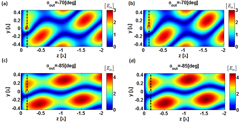
These results verify that the proposed device is capable of implementing highly-efficient anomalous reflection for a broad range of angles, properly described by an analytical model that allows full design of a PCB fabrication-ready metagrating structure, without requiring the usage of full-wave simulators.
IV Conclusion
To conclude, we have presented an analytical scheme for designing PCB metagratings for perfect anomalous reflection, comprising only a single meta-atom per period. The devices are composed of loaded conducting strips defined on a dielectric substrate backed by a PEC layer, thus allowing a realistic configuration suitable for production with standard (PCB) manufacturing techniques. The formulation enables evaluation of the appropriate substrate thickness and the suitable dimensions of the printed capacitor that facilitate reflection of a given incident plane wave towards a desirable non-specular direction. This is achieved using considerations of destructive interference phenomena to eliminate spurious specular reflections, and power conservation to guarantee unitary coupling efficiencies via a passive and lossless structure.
We demonstrated that by selecting proper working points, oriented by the observations reported in previous work [22], near-optimal wide-angle anomalous reflection can be achieved even in the presence of realistic losses. Devices operating at these preferable working points often feature relatively large bandwidth, in consistency with previous theoretical reports [16, 22] and recent empirical evidence [27]. The analytical model was verified via full-wave simulations, confirming our design methodology for various design points.
Importantly, our results reveal that the detailed rigorous analytical model can generate trustworthy fabrication-ready PCB designs without any full-wave optimization whatsoever, overcoming the considerable complexity involved with metasurface physical realization, which demands numerically-intensive simulations for the implementation of dense subwavelength meta-atom arrays. These new analytical tools would facilitate efficient synthesis of detailed metagrating designs, which would allow experimental characterization in future work, and are expected to accelerate the development of advanced metagratings for versatile diffraction engineering.
Appendix A Evaluating the grid-generated fields at the reference strip
As was mentioned in section II-E, it is not possible to calculate the field generated from the grid at the reference strip by simply substituting in (17), as the summation diverges at this point. Instead, we follow the formulation steps prescribed in this appendix to evaluate the fields at this position, necessary for relating the load impedance to the currents induced by the applied fields, and thus for finalizing the metagrating design.
First, we isolate the singular components of (17), using (14) to divide it into two terms as follows
| (36) | ||||
The first term corresponds to the source fields that the grid currents induce at the reference strip position (in the absence of the substrate and PEC); it originates from (7) after applying the Poisson formula and taking . However, the Hankel function diverges at and therefore this transformation is not applicable at this point.
Hence, we retrace our steps and utilize the original form (7) for the field assessment. This is achieved by following [28], separating the Hankel function summation into the self-induced fields that the reference wire creates on its shell (), and the field generated by all the other strips at the position of the reference strip, reading
| (37) | ||||
As in [28, 22], the first term in (37) can be approximated by the asymptotic expression of the Hankel function for small arguments as per Eq. (9.1.8) in [34] (recall that ), while the second term can be expanded using Eq. (8.522) in [35]. The last term corresponds to the field induced on the reference strip due to the reflections of the grid-generated field from the PEC-backed dielectric; it can be interpreted as the field due to multiple image sources positioned at [29], thus does not suffer of convergence issues at the distant reference strip, and can be evaluated directly. Applying these transformations onto (37) and rearranging the terms leads to (30).
References
- [1] N. Yu, P. Genevet, M. A. Kats, F. Aieta, J.-P. Tetienne, F. Capasso, and Z. Gaburro, “Light propagation with phase discontinuities: generalized laws of reflection and refraction,” Science, vol. 334, no. 6054, pp. 333–337, 2011.
- [2] S. Sun, Q. He, S. Xiao, Q. Xu, X. Li, and L. Zhou, “Gradient-index meta-surfaces as a bridge linking propagating waves and surface waves,” Nat. Mater., vol. 11, no. 5, p. 426, 2012.
- [3] C. Pfeiffer and A. Grbic, “Metamaterial huygens’ surfaces: tailoring wave fronts with reflectionless sheets,” Phys. Rev. Lett., vol. 110, no. 19, p. 197401, 2013.
- [4] M. Selvanayagam and G. V. Eleftheriades, “Discontinuous electromagnetic fields using orthogonal electric and magnetic currents for wavefront manipulation,” Opt. Express, vol. 21, no. 12, pp. 14 409–14 429, June 2013.
- [5] A. Epstein and G. V. Eleftheriades, “Passive lossless huygens metasurfaces for conversion of arbitrary source field to directive radiation,” IEEE Trans. Antennas Propag., vol. 62, no. 11, pp. 5680–5695, 2014.
- [6] C. Pfeiffer, C. Zhang, V. Ray, L. J. Guo, and A. Grbic, “High performance bianisotropic metasurfaces: asymmetric transmission of light,” Phys. Rev. Lett., vol. 113, no. 2, p. 023902, 2014.
- [7] V. Asadchy, Y. Ra’di, J. Vehmas, and S. Tretyakov, “Functional metamirrors using bianisotropic elements,” Phys. Rev. Lett., vol. 114, no. 9, p. 095503, 2015.
- [8] K. Achouri, M. A. Salem, and C. Caloz, “General metasurface synthesis based on susceptibility tensors,” IEEE Trans. Antennas Propag., vol. 63, no. 7, pp. 2977–2991, 2015.
- [9] A. Epstein and G. V. Eleftheriades, “Huygens’ metasurfaces via the equivalence principle: design and applications,” J. Opt. Soc. Am. B, vol. 33, no. 2, pp. A31–A50, 2016.
- [10] ——, “Arbitrary power-conserving field transformations with passive lossless omega-type bianisotropic metasurfaces,” IEEE Trans. Antennas Propag., vol. 64, no. 9, pp. 3880–3895, 2016.
- [11] ——, “Synthesis of passive lossless metasurfaces using auxiliary fields for reflectionless beam splitting and perfect reflection,” Phys. Rev. Lett., vol. 117, no. 25, p. 256103, 2016.
- [12] V. Asadchy, M. Albooyeh, S. Tcvetkova, A. Díaz-Rubio, Y. Ra’di, and S. Tretyakov, “Perfect control of reflection and refraction using spatially dispersive metasurfaces,” Phys. Rev. B, vol. 94, no. 7, p. 075142, 2016.
- [13] N. M. Estakhri and A. Alù, “Wave-front transformation with gradient metasurfaces,” Phys. Rev. X, vol. 6, no. 4, p. 041008, 2016.
- [14] A. Epstein, J. P. Wong, and G. V. Eleftheriades, “Cavity-excited huygens’ metasurface antennas for near-unity aperture illumination efficiency from arbitrarily large apertures,” Nat. Commun., vol. 7, p. 10360, 2016.
- [15] C. Pfeiffer and A. Grbic, “Bianisotropic metasurfaces for optimal polarization control: Analysis and synthesis,” Phys. Rev. Appl., vol. 2, no. 4, p. 044011, 2014.
- [16] Y. Ra’di, D. L. Sounas, and A. Alù, “Metagratings: Beyond the Limits of Graded Metasurfaces for Wave Front Control,” Phys. Rev. Lett., vol. 119, no. 6, p. 067404, aug 2017.
- [17] P. S. J. Russell, “Optics of floquet-bloch waves in dielectric gratings,” Appl. Phys. B: Lasers Opt., vol. 39, no. 4, pp. 231–246, 1986.
- [18] N. M. Estakhri and A. Alù, “Recent progress in gradient metasurfaces,” J. Opt. Soc. Am. B, vol. 33, no. 2, pp. A21–A30, 2016.
- [19] M. Perry, C. Shannon, E. Shults, R. Boyd, J. Britten, D. Decker, and B. Shore, “High-efficiency multilayer dielectric diffraction gratings,” Opt. Lett., vol. 20, no. 8, pp. 940–942, 1995.
- [20] N. Destouches, A. Tishchenko, J. Pommier, S. Reynaud, O. Parriaux, S. Tonchev, and M. A. Ahmed, “99% efficiency measured in the-1 st order of a resonant grating,” Opt. Express, vol. 13, no. 9, pp. 3230–3235, 2005.
- [21] H. Chalabi, Y. Ra’di, D. Sounas, and A. Alù, “Efficient anomalous reflection through near-field interactions in metasurfaces,” Phys. Rev. B, vol. 96, no. 7, p. 075432, 2017.
- [22] A. Epstein and O. Rabinovich, “Unveiling the properties of metagratings via a detailed analytical model for synthesis and analysis,” Phys. Rev. Appl., vol. 8, p. 054037, Nov 2017.
- [23] J. Yang, D. Sell, and J. A. Fan, “Freeform Metagratings Based on Complex Light Scattering Dynamics for Extreme, High Efficiency Beam Steering,” Annal. Phys., p. 1700302, oct 2017.
- [24] D. Sell, J. Yang, S. Doshay, R. Yang, and J. A. Fan, “Large-angle, multifunctional metagratings based on freeform multimode geometries,” Nano Lett., vol. 17, no. 6, pp. 3752–3757, 2017.
- [25] R. Paniagua-Dominguez, Y. F. Yu, E. Khaidarov, R. M. Bakker, X. Liang, Y. H. Fu, and A. I. Kuznetsov, “A metalens with near-unity numerical aperture,” arXiv preprint arXiv:1705.00895, 2017.
- [26] E. Khaidarov, H. Hao, R. Paniagua-Domínguez, Y. F. Yu, Y. H. Fu, V. Valuckas, S. L. K. Yap, Y. T. Toh, J. S. K. Ng, and A. I. Kuznetsov, “Asymmetric nanoantennas for ultrahigh angle broadband visible light bending,” Nano Lett., vol. 17, no. 10, pp. 6267–6272, 2017.
- [27] A. M. Wong and G. V. Eleftheriades, “Perfect anomalous reflection with a binary huygens’ metasurface,” arXiv preprint arXiv:1709.04990, 2017.
- [28] S. Tretyakov, Analytical modeling in applied electromagnetics. Artech House, 2003.
- [29] L. B. Felsen and N. Marcuvitz, Radiation and scattering of waves. John Wiley & Sons, 1994, vol. 31.
- [30] J. R. Wait, “The impedance of a wire grid parallel to a dielectric interface,” IRE Tran. Microw. Theory Techn., vol. 5, no. 2, pp. 99–102, 1957.
- [31] W. C. Chew, Waves and Fields in Inhomogeneous Media. New York: Van Nostrand Reinhold, 1990.
- [32] K. C. Gupta, R. Garg, I. Bahl, and P. Bhartia, Microstrip Lines and Slotlines. Artech House, 1996.
- [33] A. B. Yakovlev, O. Luukkonen, C. R. Simovski, S. A. Tretyakov, S. Paulotto, P. Baccarelli, and G. W. Hanson, “Analytical modeling of surface waves on high impedance surfaces,” Metamaterials and Plasmonics: Fundamentals, Modelling, Applications, pp. 239–254, 2009.
- [34] M. Abramowitz and I. A. Stegun, Handbook of Mathematical Functions : with Formulas, Graphs, and Mathematical Tables. New York: Dover Publications, 1970.
- [35] I. S. Gradshtein and I. M. Ryzhik, “Table of integrals, series, and products.” Academic Press, 2015.