跳到论文正文
W Papers独立论文阅读器 arXiv:1801.00907 论文正文 计算阅读时间 · 0%
引用这篇论文根据当前论文元数据生成,正式投稿前建议核对。


License: arXiv.org perpetual non-exclusive license
arXiv:1801.00907v1 [eess.SP] 03 Jan 2018

Performance Analysis of a Scalable DC Microgrid Offering Solar Power Based Energy Access and Efficient Control for Domestic Loads

Abu Shahir Md. Khalid Hasan Affiliation: Department of Electrical
and Electronic Engineering
Daffodil International University
Dhaka, Bangladesh.
Email: khalid.eee@diu.edu.bd
   Dhiman Chowdhury Affiliation: Department of Electrical Engineering
University of South Carolina
United States of America
Email: dhiman@email.sc.edu
   Mohammad Ziaur Rahman Khan Affiliation: Department of Electrical
and Electronic Engineering
Bangladesh University of
Engineering and Technology
Dhaka, Bangladesh.
Email: zrkhan@eee.buet.ac.bd
Abstract

DC microgrids conform to distributed control of renewable energy sources which ratifies efficacious instantaneous power sharing and sustenance of energy access among different domestic Power Management Units (PMUs) along with maintaining stability of the grid voltage. In this paper design metrics and performance evaluation of a scalable DC microgrid are documented where a look-up table of generated power of a source converter complies with the distribution of efficient power sharing phenomenon among a set of two home PMUs. The source converter is connected with a Photovoltaic panel of 300 W and uses Perturb and Observation (P&O) method for executing Maximum Power Point Tracking (MPPT). A boost average DC-DC converter topology is used to enhance the voltage level of the source converter before transmission. The load converter consists of two parallely connected PMUs each of which is constructed with high switching frequency based Full Bridge (FB) converter to charge an integrated Energy Storage System (ESS). In this paper the overall system is modeled and simulated on MATLAB/Simulink platform with ESSs in the form of Lead Acid batteries connected to the load side of the FB converter circuits and these batteries yield to support marginalized power utilities. The behaviour of the system is tested in different solar insolation levels along with several battery charging levels of 12 V and 36 V to assess the power efficiency. In each testbed the efficiency is found to be more than 93% which affirm the reliability of the framework and a look-up table is generated comprising the grid and load quantities for effective control of power transmission.

Index Terms: 
Boost average DC-DC converter, FB converter, look-up table, MPPT, PMU, power sharing, scalable DC microgrid, solar insolation level

I Introduction

Energy poverty is a common problem in many areas around the world. Fossil fuel has deleterious effects on the environment and a major concern for the current situation of global warming. A viable alternative to provide clean energy to the remote places could be the DC microgrid system. Number of people lacking electricity-access is dwindling in Latin America, North Africa, Middle East, South Asia, China and East Asia but it is still on the increase in some places like Sub-Saharian Africa. This population will remain unchanged through 2030 based on International Energy Agency (IEA) projection[1]. The price of PV components is also falling over the last few years. In addition, more compact and modular design of PV has made the system more acceptable for remote and rural regions. Decentralized electricity generation is imperative because extension of the grid in the remote regions demands extravagant connection cost [2]. Solar lantern has been used to harness solar energy for lighting and battery charging while solar home system has addressed the electricity need of an individual household in the rural and remote regions [3]. But solar lantern and solar home system cannot take advantage of multiplexing power generation or storage among several interconnected households. Microgrid brings into contact multiple households and maneuvers one or more generation sources. Microgrid can be a part of larger microgrid or run on recluse islanded-mode. While solar home system needs to be designed for peak load of the household, microgrid can be contrived for the peak demand of the community which will be more cost efficient[4]. A diesel generator can be used as another generation source when the irradiation level is unsatisfactory. Grid connectivity can be considered as another source of generation[5]. The fact that microgrid can manipulate power over the interconnected households infuses confidence for its usage. DC microgrid uses distributed Point-Of-Load (POL) converters which is much more efficient than always-on central inverters because plethora of DC appliances are utilized in the remote and rural regions. In AC microgrid, inverters experience grid-wide brownouts when correlated peaks are observed on the load[6]. DC microgrid with local storage provides energy individulally to each house hold negating this effect. Again, the overall efficiency suffers in case of low demand in AC microgrids; whereas the distributed storage system provides better resemblance in case of average demand for the power converters. The DC-AC conversion losses in the inverters and the central battery bank is more than the DC-DC conversion and distributed battery system used in the DC microgrid [9]-[11].

In this paper, a DC microgrid is simulated where a boost average DC-DC converter is guided by MPPT and then FB converter is used to bring down the voltage to battery level. The system is monitored for distinctive solar insolation levels along with separable load ratings and found to work at similar efficiency. The efficiency is also found to be stable in various loading conditions of the PMUs and different switching frequencies of FB converter. The overall scalable microgrid architecture is evaluated in regard to power sharing in a set of two PMUs. Each PMU supports a battery intended to transmit consistent power to attached loads like home appliances. This paper concerns with equal and different power sharing between two PMUs to assess power efficiency and reliable power transmission from the source converter to the load side. In the follow-up, an adaptive look-up table has been generated comprising the evaluated power quantities and performance parameters for different switching frequencies and battery voltage levels. The proposed microgrid architecture, PMU circuit configuration and its operation, simulated profiles of microgrid’s operation, generated look-up table and a brief explanation of the overall implemented system are articulated in this paper section-by-section.

Refer to caption
Fig. 1: Proposed DC microgrid architecture in MATLAB/ Simulink
Refer to caption
Fig. 2: PMU circuit structure in MATLAB/ Simulink

II Proposed DC Microgrid Architecture

The PV array acts as a constant current source. Based on irradiation level, the perturb and observation method tracks the maximum power point and generates the duty cycle required for the boost average DC-DC converter to level up the voltage. The PMU consists of a FB converter where MOSFETs are used as the switching devices. The main purpose is to monitor the equal and unequal load sharing of the PMUs and then generate an adaptive look up table for which the power source can be utilized accordingly.

II-A Perturb and Observation Algorithm based MPPT Control

Maximum Power Point Tracking (MPPT) is a methodology used in photovoltaic (PV) converters to continuously adjust the impedance seen by the solar array to keep the PV system operating at, or close to, the peak power point of the PV panel under varying conditions, like changing solar irradiance, temperature, and load.

The algorithm senses the voltage V⁡(k)\mathchar 29014\delimiter 67273472\mathchar 29035\delimiter 84054785 and current I⁡(k)\mathchar 29001\delimiter 67273472\mathchar 29035\delimiter 84054785 to measure the instantaneous power P⁡(k)\mathchar 29008\delimiter 67273472\mathchar 29035\delimiter 84054785 at the kt​h\mathchar 29035^{\mathchar 29044\mathchar 29032} sample. Then it compares it with previous power sample P⁡(k−1)\mathchar 29008\delimiter 67273472\mathchar 29035\mathchar 8704\mathchar 28721\delimiter 84054785. If the two power samples are different then it then the voltage sample V⁡(k)\mathchar 29014\delimiter 67273472\mathchar 29035\delimiter 84054785 is compared with its previous sample V⁡(k−1)\mathchar 29014\delimiter 67273472\mathchar 29035\mathchar 8704\mathchar 28721\delimiter 84054785 and the duty cycle Db\mathchar 28996_{\mathchar 29026} of the boost converter is adjusted accordingly to ensure that the system operates at “maximum power point” (or peak voltage) on the power voltage curve, as shown below. The algorithms account for factors such as variable irradiance (sunlight) and temperature to ensure that the PV system generates maximum power at all times.
Refer to caption
Fig. 3: Boost converter average model

II-B Boost Converter Average Model

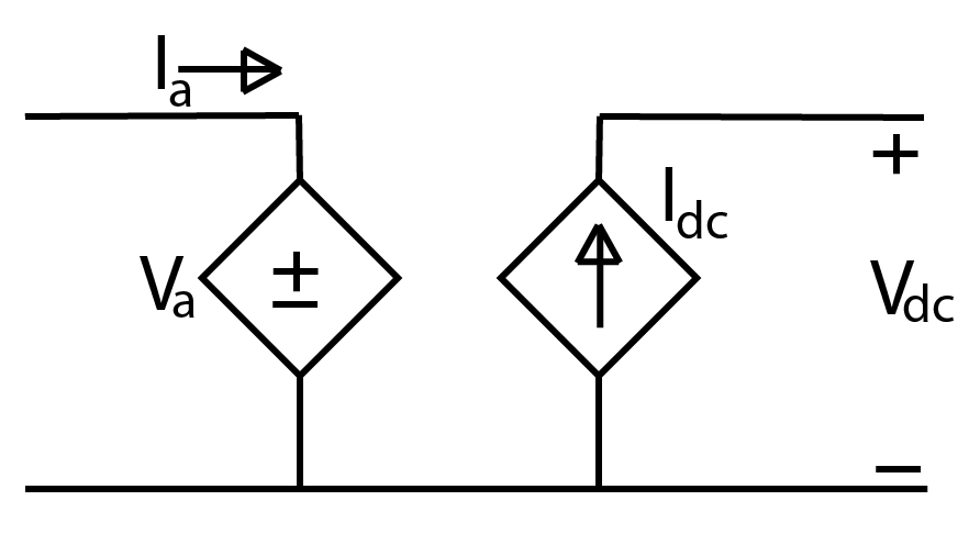
The average model for boost converter is designed with a controlled voltage source in the input and a controlled current source in the output. In Fig. 3, Va\mathchar 29014_{\mathchar 29025} and Ia\mathchar 29001_{\mathchar 29025} are the input current and voltage whereas Vd​c\mathchar 29014_{\mathchar 29028\mathchar 29027} and Id​c\mathchar 29001_{\mathchar 29028\mathchar 29027} are the output current and voltage of the boost converter. The equations for Va\mathchar 29014_{\mathchar 29025} and Id​c\mathchar 29001_{\mathchar 29028\mathchar 29027} are

Va​(k)=(1−Db)​Vd​c​(k−1)\mathchar 29014_{\mathchar 29025}\delimiter 67273472\mathchar 29035\delimiter 84054785\mathchar 12349\delimiter 67273472\mathchar 28721\mathchar 8704\mathchar 28996_{\mathchar 29026}\delimiter 84054785\mathchar 29014_{\mathchar 29028\mathchar 29027}\delimiter 67273472\mathchar 29035\mathchar 8704\mathchar 28721\delimiter 84054785 (1)
Id​c​(k)=(1−Db)​Vd​c​(k−2)​Ia​(k−1)2​Vd​c​(k−2)−Vd​c​(k−3)\mathchar 29001_{\mathchar 29028\mathchar 29027}\delimiter 67273472\mathchar 29035\delimiter 84054785\mathchar 12349{{\delimiter 67273472\mathchar 28721\mathchar 8704\mathchar 28996_{\mathchar 29026}\delimiter 84054785\mathchar 29014_{\mathchar 29028\mathchar 29027}\delimiter 67273472\mathchar 29035\mathchar 8704\mathchar 28722\delimiter 84054785\mathchar 29001_{\mathchar 29025}\delimiter 67273472\mathchar 29035\mathchar 8704\mathchar 28721\delimiter 84054785\over\mathchar 28722\mathchar 29014_{\mathchar 29028\mathchar 29027}\delimiter 67273472\mathchar 29035\mathchar 8704\mathchar 28722\delimiter 84054785\mathchar 8704\mathchar 29014_{\mathchar 29028\mathchar 29027}\delimiter 67273472\mathchar 29035\mathchar 8704\mathchar 28723\delimiter 84054785}} (2)
Refer to caption
Fig. 4: Circuit diagram of the PMU Block and the control switch pattern
Refer to caption
Fig. 5: Inductive voltage pattern considering ideal active and passive switches
Refer to caption
Fig. 6: PMU circuit operation analysis considering non-ideal active and passive switches; (a) PMU in switch position-1 and (b) PMU in switch position-2
Refer to caption
Fig. 7: Inductive voltage pattern considering non-ideal active and passive Switches

II-C PMU Circuit Operation Analysis

II-C1 Ideal Active and Passive Switches

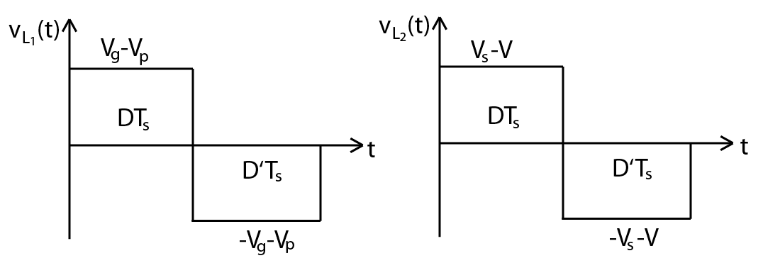
The MOSFETs in the PMUs are the active switches and each has an internal diode paralleled with a RC snubber circuit. When a gate signal is applied to the MOSFET it acts as the switch on-resistance and when the gate signal is turned off the current moves through the anti-parallel diode. Vg\mathchar 29014_{\mathchar 29031} is the input voltage for the PMUs and the control switch are delineated as 1 and 2 inside a circle in 4. A linear transformer is used to lower the voltage into desired level as well as provide electrical isolation. The four diodes D1\mathchar 28996_{\mathchar 28721},D2\mathchar 28996_{\mathchar 28722},D3\mathchar 28996_{\mathchar 28723} and D4\mathchar 28996_{\mathchar 28724} are the passive switches. The Ll​k\mathchar 29004_{\mathchar 29036\mathchar 29035} models the leakage inductance and has a damping effect on the circuit. The change in current through the output inductor Lo​u​t\mathchar 29004_{\mathchar 29039\mathchar 29045\mathchar 29044}, and the change in voltage across the output capacitor Co​u​t\mathchar 28995_{\mathchar 29039\mathchar 29045\mathchar 29044} are small compared through their nominal values over a switching period [7]-[9]. Considering the control switch pattern in Fig. 4, D+D​′=1\mathchar 28996\mathchar 8235\mathchar 28996\raise 3.44444pt\hbox{\sevensy\char 48\relax}\mathchar 12349\mathchar 28721 at switch position 1 during D​Ts\mathchar 28996\mathchar 29012_{\mathchar 29043} subinterval

VL1=Vg−Vp​a​n​d​VL2=Vs−V\mathchar 29014_{\mathchar 29004_{\mathchar 28721}}\mathchar 12349\mathchar 29014_{\mathchar 29031}\mathchar 8704\mathchar 29014_{\mathchar 29040}\hskip 5.0pt\mathchar 29025\mathchar 29038\mathchar 29028\hskip 5.0pt\mathchar 29014_{\mathchar 29004_{\mathchar 28722}}\mathchar 12349\mathchar 29014_{\mathchar 29043}\mathchar 8704\mathchar 29014 (3)

at switch position 2 during D​′​Ts\mathchar 28996\raise 3.44444pt\hbox{\sevensy\char 48\relax}\mathchar 29012_{\mathchar 29043} subinterval

VL1=−Vg−Vp​a​n​d​VL2=−Vs−V\mathchar 29014_{\mathchar 29004_{\mathchar 28721}}\mathchar 12349\mathchar 8704\mathchar 29014_{\mathchar 29031}\mathchar 8704\mathchar 29014_{\mathchar 29040}\hskip 5.0pt\mathchar 29025\mathchar 29038\mathchar 29028\hskip 5.0pt\mathchar 29014_{\mathchar 29004_{\mathchar 28722}}\mathchar 12349\mathchar 8704\mathchar 29014_{\mathchar 29043}\mathchar 8704\mathchar 29014 (4)
Refer to caption
Fig. 8: Input-to-output port of the PMU circuit acting in non-ideal switching mode
Refer to caption
Fig. 9: Simulation results for 1​2​V\mathchar 28721\mathchar 28722\mathchar 29014 batteries with same and different capacity in two separate PMUs in 5​0​k​H​z\mathchar 28725\mathchar 28720\mathchar 29035\mathchar 29000\mathchar 29050 switching frequency for the active switches. The irradiance pattern was kept identical for each case. The green dotted line represents the case when the two separate PMUs have same battery capacity while the blue solid line depicts the case with two different battery capacity in two separate PMUs.
Refer to caption
Fig. 10: Simulation results for 3​6​V\mathchar 28723\mathchar 28726\mathchar 29014 batteries with same and different capacity in two separate PMUs in 5​0​k​H​z\mathchar 28725\mathchar 28720\mathchar 29035\mathchar 29000\mathchar 29050 switching frequency for the active switches. The irradiance pattern was kept identical for each case. The green dotted line represents the case when the two separate PMUs have same battery capacity while the blue solid line depicts the case with two different battery capacity in two separate PMUs.

in both cases, small ripple approximation is considered here,

Vp=n​Vs\mathchar 29014_{\mathchar 29040}\mathchar 12349\mathchar 29038\mathchar 29014_{\mathchar 29043} (5)

Using volt-sec balance for inductor Ll​k\mathchar 29004_{\mathchar 29036\mathchar 29035} and Lo​u​t\mathchar 29004_{\mathchar 29039\mathchar 29045\mathchar 29044} taking equation (3), (4) and (5)

(Vg−n​Vs)​D+(−Vg−n​Vs)​D​′=0\delimiter 67273472\mathchar 29014_{\mathchar 29031}\mathchar 8704\mathchar 29038\mathchar 29014_{\mathchar 29043}\delimiter 84054785\mathchar 28996\mathchar 8235\delimiter 67273472\mathchar 8704\mathchar 29014_{\mathchar 29031}\mathchar 8704\mathchar 29038\mathchar 29014_{\mathchar 29043}\delimiter 84054785\mathchar 28996\raise 3.44444pt\hbox{\sevensy\char 48\relax}\mathchar 12349\mathchar 28720
Vs=1n​Vg​(2​D−1)\mathchar 29014_{\mathchar 29043}\mathchar 12349{{\mathchar 28721\over\mathchar 29038}}\mathchar 29014_{\mathchar 29031}\delimiter 67273472\mathchar 28722\mathchar 28996\mathchar 8704\mathchar 28721\delimiter 84054785 (6)
(Vs−V)​D+(−Vs−V)​D​′=0\delimiter 67273472\mathchar 29014_{\mathchar 29043}\mathchar 8704\mathchar 29014\delimiter 84054785\mathchar 28996\mathchar 8235\delimiter 67273472\mathchar 8704\mathchar 29014_{\mathchar 29043}\mathchar 8704\mathchar 29014\delimiter 84054785\mathchar 28996\raise 3.44444pt\hbox{\sevensy\char 48\relax}\mathchar 12349\mathchar 28720
Vs​(2​D−1)=V\mathchar 29014_{\mathchar 29043}\delimiter 67273472\mathchar 28722\mathchar 28996\mathchar 8704\mathchar 28721\delimiter 84054785\mathchar 12349\mathchar 29014

from (6), voltage gain,

M⁡(D)=VVg=1n​(2​D−1)2\mathchar 29005\delimiter 67273472\mathchar 28996\delimiter 84054785\mathchar 12349{{\mathchar 29014\over\mathchar 29014_{\mathchar 29031}}}\mathchar 12349{{\mathchar 28721\over\mathchar 29038}}\delimiter 67273472\mathchar 28722\mathchar 28996\mathchar 8704\mathchar 28721\delimiter 84054785^{\mathchar 28722} (7)

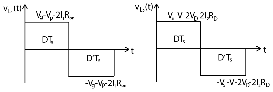
II-C2 Active and Passive Switches with Semiconductor Losses

At switch 1

VL1=Vg−Vp−2​I1​Ro​n\mathchar 29014_{\mathchar 29004_{\mathchar 28721}}\mathchar 12349\mathchar 29014_{\mathchar 29031}\mathchar 8704\mathchar 29014_{\mathchar 29040}\mathchar 8704\mathchar 28722\mathchar 29001_{\mathchar 28721}\mathchar 29010_{\mathchar 29039\mathchar 29038} (8)
VL2=Vs−V−VD−2​I2​Ro​n\mathchar 29014_{\mathchar 29004_{\mathchar 28722}}\mathchar 12349\mathchar 29014_{\mathchar 29043}\mathchar 8704\mathchar 29014\mathchar 8704\mathchar 29014_{\mathchar 28996}\mathchar 8704\mathchar 28722\mathchar 29001_{\mathchar 28722}\mathchar 29010_{\mathchar 29039\mathchar 29038} (9)

At switch 2

VL1=−Vg−Vp−2​I1​Ro​n\mathchar 29014_{\mathchar 29004_{\mathchar 28721}}\mathchar 12349\mathchar 8704\mathchar 29014_{\mathchar 29031}\mathchar 8704\mathchar 29014_{\mathchar 29040}\mathchar 8704\mathchar 28722\mathchar 29001_{\mathchar 28721}\mathchar 29010_{\mathchar 29039\mathchar 29038} (10)
VL2=−Vs−V−2​VD−2​I2​Ro​n\mathchar 29014_{\mathchar 29004_{\mathchar 28722}}\mathchar 12349\mathchar 8704\mathchar 29014_{\mathchar 29043}\mathchar 8704\mathchar 29014\mathchar 8704\mathchar 28722\mathchar 29014_{\mathchar 28996}\mathchar 8704\mathchar 28722\mathchar 29001_{\mathchar 28722}\mathchar 29010_{\mathchar 29039\mathchar 29038} (11)

Now using volt-second balance for L1\mathchar 29004_{\mathchar 28721} and L2\mathchar 29004_{\mathchar 28722} and Vp=n​VS\mathchar 29014_{\mathchar 29040}\mathchar 12349\mathchar 29038\mathchar 29014_{\mathchar 29011} and I2=I1\mathchar 29001_{\mathchar 28722}\mathchar 12349\mathchar 29001_{\mathchar 28721}

(Vg−Vp−2​I1​Ro​n)​D+(−Vg−Vp−2​I1​Ro​n)​D​′=0\delimiter 67273472\mathchar 29014_{\mathchar 29031}\mathchar 8704\mathchar 29014_{\mathchar 29040}\mathchar 8704\mathchar 28722\mathchar 29001_{\mathchar 28721}\mathchar 29010_{\mathchar 29039\mathchar 29038}\delimiter 84054785\mathchar 28996\mathchar 8235\delimiter 67273472\mathchar 8704\mathchar 29014_{\mathchar 29031}\mathchar 8704\mathchar 29014_{\mathchar 29040}\mathchar 8704\mathchar 28722\mathchar 29001_{\mathchar 28721}\mathchar 29010_{\mathchar 29039\mathchar 29038}\delimiter 84054785\mathchar 28996\raise 3.44444pt\hbox{\sevensy\char 48\relax}\mathchar 12349\mathchar 28720
Vg​(2​D−1)−2​I1​Ro​n=n​Vs\mathchar 29014_{\mathchar 29031}\delimiter 67273472\mathchar 28722\mathchar 28996\mathchar 8704\mathchar 28721\delimiter 84054785\mathchar 8704\mathchar 28722\mathchar 29001_{\mathchar 28721}\mathchar 29010_{\mathchar 29039\mathchar 29038}\mathchar 12349\mathchar 29038\mathchar 29014_{\mathchar 29043}
Vs=1n​[Vg​(2​D−1)−2​I1​Ro​n]\mathchar 29014_{\mathchar 29043}\mathchar 12349{{\mathchar 28721\over\mathchar 29038}}\delimiter 67482370\mathchar 29014_{\mathchar 29031}\delimiter 67273472\mathchar 28722\mathchar 28996\mathchar 8704\mathchar 28721\delimiter 84054785\mathchar 8704\mathchar 28722\mathchar 29001_{\mathchar 28721}\mathchar 29010_{\mathchar 29039\mathchar 29038}\delimiter 84267779 (12)

and

(Vs−V−2​VD−2​I2​RD)​D+(−Vs−V−2​VD−2​I2​RD)​D​′=0\delimiter 67273472\mathchar 29014_{\mathchar 29043}\mathchar 8704\mathchar 29014\mathchar 8704\mathchar 28722\mathchar 29014_{\mathchar 28996}\mathchar 8704\mathchar 28722\mathchar 29001_{\mathchar 28722}\mathchar 29010_{\mathchar 28996}\delimiter 84054785\mathchar 28996\mathchar 8235\delimiter 67273472\mathchar 8704\mathchar 29014_{\mathchar 29043}\mathchar 8704\mathchar 29014\mathchar 8704\mathchar 28722\mathchar 29014_{\mathchar 28996}\mathchar 8704\mathchar 28722\mathchar 29001_{\mathchar 28722}\mathchar 29010_{\mathchar 28996}\delimiter 84054785\mathchar 28996\raise 3.44444pt\hbox{\sevensy\char 48\relax}\mathchar 12349\mathchar 28720
Vs​(2​D−1)=V+2​VD+2​I2​RD\mathchar 29014_{\mathchar 29043}\delimiter 67273472\mathchar 28722\mathchar 28996\mathchar 8704\mathchar 28721\delimiter 84054785\mathchar 12349\mathchar 29014\mathchar 8235\mathchar 28722\mathchar 29014_{\mathchar 28996}\mathchar 8235\mathchar 28722\mathchar 29001_{\mathchar 28722}\mathchar 29010_{\mathchar 28996}
1n​[Vg​(2​D−1)−2​I1​Ro​n]​(2​D−1)=V+2​VD+2​I2​RD{{\mathchar 28721\over\mathchar 29038}}\delimiter 67482370\mathchar 29014_{\mathchar 29031}\delimiter 67273472\mathchar 28722\mathchar 28996\mathchar 8704\mathchar 28721\delimiter 84054785\mathchar 8704\mathchar 28722\mathchar 29001_{\mathchar 28721}\mathchar 29010_{\mathchar 29039\mathchar 29038}\delimiter 84267779\delimiter 67273472\mathchar 28722\mathchar 28996\mathchar 8704\mathchar 28721\delimiter 84054785\mathchar 12349\mathchar 29014\mathchar 8235\mathchar 28722\mathchar 29014_{\mathchar 28996}\mathchar 8235\mathchar 28722\mathchar 29001_{\mathchar 28722}\mathchar 29010_{\mathchar 28996}
1n​Vg​(2​D−1)2=2n​I1​Ro​n​(2​D−1)+V+2​VD+2​n​I1​RD{{\mathchar 28721\over\mathchar 29038}}\mathchar 29014_{\mathchar 29031}\delimiter 67273472\mathchar 28722\mathchar 28996\mathchar 8704\mathchar 28721\delimiter 84054785^{\mathchar 28722}\mathchar 12349{{\mathchar 28722\over\mathchar 29038}}\mathchar 29001_{\mathchar 28721}\mathchar 29010_{\mathchar 29039\mathchar 29038}\delimiter 67273472\mathchar 28722\mathchar 28996\mathchar 8704\mathchar 28721\delimiter 84054785\mathchar 8235\mathchar 29014\mathchar 8235\mathchar 28722\mathchar 29014_{\mathchar 28996}\mathchar 8235\mathchar 28722\mathchar 29038\mathchar 29001_{\mathchar 28721}\mathchar 29010_{\mathchar 28996} (13)

From (13)

1n​Vg​(2​D−1)2​[1−2​I1​Ro​nVg​(2​D−1)−2​n​VDVg​(2​D−1)2−2​n2​I1​RDVg​(2​D−1)2]=V{{\mathchar 28721\over\mathchar 29038}}\mathchar 29014_{\mathchar 29031}\delimiter 67273472\mathchar 28722\mathchar 28996\mathchar 8704\mathchar 28721\delimiter 84054785^{\mathchar 28722}\delimiter 67482370\mathchar 28721\mathchar 8704{{\mathchar 28722\mathchar 29001_{\mathchar 28721}\mathchar 29010_{\mathchar 29039\mathchar 29038}\over\mathchar 29014_{\mathchar 29031}\delimiter 67273472\mathchar 28722\mathchar 28996\mathchar 8704\mathchar 28721\delimiter 84054785}}\mathchar 8704{{\mathchar 28722\mathchar 29038\mathchar 29014_{\mathchar 28996}\over\mathchar 29014_{\mathchar 29031}\delimiter 67273472\mathchar 28722\mathchar 28996\mathchar 8704\mathchar 28721\delimiter 84054785^{\mathchar 28722}}}\mathchar 8704{{\mathchar 28722\mathchar 29038^{\mathchar 28722}\mathchar 29001_{\mathchar 28721}\mathchar 29010_{\mathchar 28996}\over\mathchar 29014_{\mathchar 29031}\delimiter 67273472\mathchar 28722\mathchar 28996\mathchar 8704\mathchar 28721\delimiter 84054785^{\mathchar 28722}}}\delimiter 84267779\mathchar 12349\mathchar 29014

Now, voltage gain,

M​′​(D)=VVg=M⁡(D)​[1−2​I1​Ro​nVg​(2​D−1)−2​n​VDVg​(2​D−1)2−2​n2​I1​RDVg​(2​D−1)2]\mathchar 29005\raise 3.44444pt\hbox{\sevensy\char 48\relax}\delimiter 67273472\mathchar 28996\delimiter 84054785\mathchar 12349{{\mathchar 29014\over\mathchar 29014_{\mathchar 29031}}}\mathchar 12349\mathchar 29005\delimiter 67273472\mathchar 28996\delimiter 84054785\delimiter 67482370\mathchar 28721\mathchar 8704{{\mathchar 28722\mathchar 29001_{\mathchar 28721}\mathchar 29010_{\mathchar 29039\mathchar 29038}\over\mathchar 29014_{\mathchar 29031}\delimiter 67273472\mathchar 28722\mathchar 28996\mathchar 8704\mathchar 28721\delimiter 84054785}}\mathchar 8704{{\mathchar 28722\mathchar 29038\mathchar 29014_{\mathchar 28996}\over\mathchar 29014_{\mathchar 29031}\delimiter 67273472\mathchar 28722\mathchar 28996\mathchar 8704\mathchar 28721\delimiter 84054785^{\mathchar 28722}}}\mathchar 8704{{\mathchar 28722\mathchar 29038^{\mathchar 28722}\mathchar 29001_{\mathchar 28721}\mathchar 29010_{\mathchar 28996}\over\mathchar 29014_{\mathchar 29031}\delimiter 67273472\mathchar 28722\mathchar 28996\mathchar 8704\mathchar 28721\delimiter 84054785^{\mathchar 28722}}}\delimiter 84267779 (14)

III Results and Analysis

TABLE I: Performance Analysis of the Microgrid Architecture for Different Switching Frequencies and Battery Ratings
Switching Battery Irradiance PV Array Source Converter MPPT PMU1 PMU2 Efficiency
Frequency (W/mˆ2) V I V I P˙mean Duty V I P˙mean V I P˙mean (Percent)
Cycle
100 kHz 12V 5.4Ah 1000 51.88 5.798 99.09 3.033 300.8 0.4768 13.02 10.81 140.7 13.02 10.81 140.7 93.55
12V 5.4Ah 1000 51.88 5.798 98.28 3.059 300.8 0.4724 12.96 9.485 122.9 12.75 12.40 158.1 93.41
12V 10.8 Ah
36V 5.4Ah 1000 51.87 5.799 115.6 2.600 300.8 0.5516 37.61 3.757 141.3 37.61 3.757 141.3 93.95
36V 5.4Ah 1000 51.88 5.798 114.9 2.616 300.8 0.5486 37.57 3.511 131.9 37.12 4.056 150.6 93.92
36V 10.8 Ah
50 kHz 12V 5.4Ah 1000 51.89 5.797 99.94 3.007 300.8 0.4810 13.02 10.83 141.0 13.02 10.83 141.0 93.55
12V 5.4Ah 1000 51.92 5.793 98.82 3.042 300.8 0.4749 12.95 9.363 121.3 12.75 12.56 160.2 93.41
12V 10.8 Ah
36V 5.4Ah 1000 51.88 5.797 106.3 2.827 300.8 0.5123 37.65 3.721 140.1 37.65 3.721 140.1 93.95
36V 5.4Ah 1000 51.92 5.793 106.4 2.824 300.8 0.5122 37.65 3.728 140.4 37.12 3.780 140.4 93.92
36V 10.8 Ah

The DC microgrid structure is simulated using MATLAB 2017a Simulink. SunPower SPR-315E-WHT-D Module which follows NREL (National Renewable Energy Laboratory) System Advisor Model (Jan. 2014), is used as the PV module which takes two inputs of Sun irradiance and Cell temperature. At 1​0​0​0​W/m2\mathchar 28721\mathchar 28720\mathchar 28720\mathchar 28720\mathchar 29015\delimiter 68408078\mathchar 29037^{\mathchar 28722} and 4​0\mathchar 28724\mathchar 28720 deg. Celsius the maximum power point is 3​0​0.8​W\mathchar 28723\mathchar 28720\mathchar 28720\mathchar 314\mathchar 28728\mathchar 29015. Inside the source converter block, a MPPT Control and a Boost average converter are employed to achieve the maximum power point as well as boosting the voltage before transmission. The MPPT control uses Perturb and Observation (P&O) algorithm which takes instantaneous voltage and current of the solar module as the input. There is a enable pin in the MPPT block which is switched to 1 to allow the continuous opetation of the algorithm. Four other control parameters for P&O algorithm are Initial value for Db\mathchar 28996_{\mathchar 29026} output (Dbi​n​i​t\mathchar 28996_{\mathchar 29026_{\mathchar 29033\mathchar 29038\mathchar 29033\mathchar 29044}}), Upper limit for Db\mathchar 28996_{\mathchar 29026} (Dbm​a​x\mathchar 28996_{\mathchar 29026_{\mathchar 29037\mathchar 29025\mathchar 29048}}), Lower limit for Db\mathchar 28996_{\mathchar 29026} (Dbm​i​n\mathchar 28996_{\mathchar 29026_{\mathchar 29037\mathchar 29033\mathchar 29038}}), Increment value used to increase/decrease (Δ​Db\mathchar 28673\mathchar 28996_{\mathchar 29026}) where Db\mathchar 28996_{\mathchar 29026} is the Boost converter duty cycle.The boost converter uses the output duty cycle of the PO and generates the desired voltage realizing (2) and (1). A constant of 1​0−6\mathchar 28721\mathchar 28720^{\mathchar 8704\mathchar 28726} is used to avoid the divide by zero condition in (1). Inside the PMUs, the value of leakage inductance Ll​k\mathchar 29004_{\mathchar 29036\mathchar 29035}, outer inductance Lo​u​t\mathchar 29004_{\mathchar 29039\mathchar 29045\mathchar 29044} and the outer capacitance is 2​6​μ​H\mathchar 28722\mathchar 28726\mathchar 28950\mathchar 29000, 1​0​μ​H\mathchar 28721\mathchar 28720\mathchar 28950\mathchar 29000 and 7​5​0​0​μ​F\mathchar 28727\mathchar 28725\mathchar 28720\mathchar 28720\mathchar 28950\mathchar 28998. The nominal power of the linear transformer is set to 150 VA in case of equal loads and frequency is adjusted according to the switching frequency of the active switches. The MOSFETs’ on-resistance Ro​n\mathchar 29010_{\mathchar 29039\mathchar 29038} and diode resistance RD\mathchar 29010_{\mathchar 28996} has the value 0.1​Ω\mathchar 28720\mathchar 314\mathchar 28721\mathchar 28682 and 0.0​1​Ω\mathchar 28720\mathchar 314\mathchar 28720\mathchar 28721\mathchar 28682 respectively. Lead acid battery is used with nominal voltage of 1​2​V\mathchar 28721\mathchar 28722\mathchar 29014, rated capacity 5.4​A​h\mathchar 28725\mathchar 314\mathchar 28724\mathchar 28993\mathchar 29032, initial state of charge 7​5%\mathchar 28727\mathchar 28725\% and battery response time is 5​0​m​i​n\mathchar 28725\mathchar 28720\mathchar 29037\mathchar 29033\mathchar 29038. The irradiation was varied from 1​0​0​0​W/m2\mathchar 28721\mathchar 28720\mathchar 28720\mathchar 28720\mathchar 29015\delimiter 68408078\mathchar 29037^{\mathchar 28722} to 5​0​0​W/m2\mathchar 28725\mathchar 28720\mathchar 28720\mathchar 29015\delimiter 68408078\mathchar 29037^{\mathchar 28722}, 5​0​0​W/m2\mathchar 28725\mathchar 28720\mathchar 28720\mathchar 29015\delimiter 68408078\mathchar 29037^{\mathchar 28722} to 5​0​W/m2\mathchar 28725\mathchar 28720\mathchar 29015\delimiter 68408078\mathchar 29037^{\mathchar 28722} and then back to 1​0​0​0​W/m2\mathchar 28721\mathchar 28720\mathchar 28720\mathchar 28720\mathchar 29015\delimiter 68408078\mathchar 29037^{\mathchar 28722} from 5​0​W/m2\mathchar 28725\mathchar 28720\mathchar 29015\delimiter 68408078\mathchar 29037^{\mathchar 28722} for 1​2​V\mathchar 28721\mathchar 28722\mathchar 29014 and 3​6​V\mathchar 28723\mathchar 28726\mathchar 29014 batteries with same and different battery capacity in two different switching frequencies of 5​0​k​H​z\mathchar 28725\mathchar 28720\mathchar 29035\mathchar 29000\mathchar 29050 and 1​0​0​k​H​z\mathchar 28721\mathchar 28720\mathchar 28720\mathchar 29035\mathchar 29000\mathchar 29050. Fig. 9 shows the simulation results for 1​2​V\mathchar 28721\mathchar 28722\mathchar 29014 batteries with same and different capacity in two separate PMUs in 1​0​0​k​H​z\mathchar 28721\mathchar 28720\mathchar 28720\mathchar 29035\mathchar 29000\mathchar 29050 switching frequency for the active switches. The output voltage of the source converter tends to show minor change due to fluctuation of the irradiance which is very encouraging. The average power is divided into PMUs equally when the battery parameters are uniform. The battery with higher rated capacity draws higher power resulting in unequal power sharing between the two PMUs although the source converter output voltage is almost the same as the former case. The average power from the PV array and the sum of the average power of the PMUs are very closely matched in both cases and proportionate to the irradiance pattern. An interesting observation is that when the irradiance jumps back to 1​0​0​0​W/m2\mathchar 28721\mathchar 28720\mathchar 28720\mathchar 28720\mathchar 29015\delimiter 68408078\mathchar 29037^{\mathchar 28722} from 5​0​W/m2\mathchar 28725\mathchar 28720\mathchar 29015\delimiter 68408078\mathchar 29037^{\mathchar 28722} the average power slows down to move to 3​0​0.8\mathchar 28723\mathchar 28720\mathchar 28720\mathchar 314\mathchar 28728 towards the end.

Table I shows the simulation results for two different battery voltage in two disparate switching frequency. For 3​6​V\mathchar 28723\mathchar 28726\mathchar 29014 batteries the transformer ratings were adjusted to maintain the output of the PMUs to the desired level. The MPPT duty cycle moved to a different point resulting in a slightly different source converter output voltage around 1​1​0​V\mathchar 28721\mathchar 28721\mathchar 28720\mathchar 29014 but keeps average power to 3​0​0.8​W\mathchar 28723\mathchar 28720\mathchar 28720\mathchar 314\mathchar 28728\mathchar 29015. The efficiency estimated in all different cases is more than 9​3%\mathchar 28729\mathchar 28723\% which ensures the stability of the system in different battery voltage level and frequency.

IV Conclusion

The design presented in this paper is a simplified version of the scalable DC microgrid architecture. The control phenomenon of the load converter and the load side of the home PMU configuration are different from those of the generic structure proposed in [9]. Basic PMW signals are used instead of phase-shifted PWM as the switch control attributes in the PMUs. The look-up table generated from multiple simulations is an attempt to establish a one-way communication method for smart load sharing among different PMUs. One-way communication will reduce the complexities of the electrical circuits and can prove to be a cost effective solution which can have a major effect in popularizing the DC microgrid in the developing countries. Moreover, phase-shifted PWM can be implemented for zero voltage switching of the converter and practical implication of the system.

References

  • [1] ”WORLD ENERGY OUTLOOK 2011 FACTSHEET”, IEA World Energy Outlook 2011, November 2011.
  • [2] P. Alstone, D. Gershenson, and D. M. Kammen, “Decentralized energy systems for clean electricity access”, Nature Climate Change, 2015.
  • [3] S. Komatsu, S. Kaneko, and P. P. Ghosh, “Are micro-benefits negligible? The implications of the rapid expansion of Solar Home Systems (SHS) in rural Bangladesh for sustainable development”, Energy Policy, 2011.
  • [4] P. Bardouille, P. Avato, J. Levin, A. Pantelias, and H. Engelmann-Pilger, “From gap to opportunity: Business models for scaling up energy access”, International Finance Corporation, 2012
  • [5] Dushan Boroyevich, Igor Cvetkovic, Dong Dong, et al, “Future electronic power distribution systems a contemplative view” 12th International Conference on Optimization of Electrical and Electronic Equipment, pages 1369–1380. IEEE, May 2010.
  • [6] T. G. Quetchenbach, M. J. Harper, J. Robinson IV, et al., “The GridShare solution: a smart grid approach to improve service provision on a renewable energy mini-grid in Bhutan.”, Environmental Research Letters,8(1):014018, 2013.
  • [7] V. Vlatkovic, J. A. Sabate, R. B. Ridley, F. C. Lee, and B. H. Cho, “Small-Signal Analysis of the Phase-Shifted PWM Converter”, IEEE Transactions on Power Electronics,7(1),pages 128-135, January 1992.
  • [8] M. J. Schutten and D. A. Torrey, “Improved small-signal analysis for the phase-shifted PWM power converter”, IEEE Transactions on Power Electronics,vol. 18, no. 2, pp. 659–669, Mar. 2003.
  • [9] P. A. Madduri, J. Poon, J. Rosa, M. Podolsky, E. Brewer, S. Sanders, “A scalable dc microgrid architecture for rural electrification in emerging regions”, Applied Power Electronics Conference and Exposition,7(1),pages 703-708, Mar 2015.
  • [10] W. Stevens and G. P. Corey, “A study of lead-acid battery efficiency near top-of-charge and the impact on pv system design”, Photovoltaic Specialists Conference, 1996., Conference Record of the Twenty Fifth IEEE, pp. 1485–1488, 1996.
  • [11] A. C. Brent and D. E. Rogers, “Renewable rural electrification: Sustainability assessment of mini-hybrid off-grid technological systems in the African context”, Renewable Energy, vol. 35, no. 1, pp. 257–265, Jan. 2010.