Electron effective mass in unintentionally doped In0.33Ga0.67N determined by mid-infrared optical Hall effect
Abstract
Mid-infrared optical Hall effect measurements are used to determine the free charge carrier parameters of an unintentionally doped wurtzite-structure -plane oriented In0.33Ga0.67N epitaxial layer. Room temperature electron effective mass parameters of and for polarization perpendicular and parallel to the -axis, respectively, were determined. The free electron concentration was obtained as cm-3. Within our uncertainty limits we detect no anisotropy for the electron effective mass parameter and we estimate the upper limit of the possible effective mass anisotropy is 7. We discuss the influence of band nonparabolicity on the electron effective mass parameter as a function of In content. The effective mass parameter is consistent with a linear interpolation scheme between the conduction band mass parameters in GaN and InN when the strong nonparabolicity in InN is included. The In0.33Ga0.67N electron mobility parameters were found to be anisotropic supporting previous experimental findings for wurtzite-structure GaN, InN, and AlxGa1-xN epitaxial layers with -plane growth orientation.
Variation of indium content in wurtzite-structure InxGa1-xN permits tuning its bandgap from the NIR (NIR) (NIR; InN) to the UV (UV) (UV; GaN) spectral range.[1] Device heterostructures employing low-In content InxGa1-xN alloys () are widely used in blue light emitting diodes, laser diodes and vertical-cavity surface-emitting lasers. On the other hand, higher In content () InxGa1-xN optoelectronic devices for operation at long wavelengths are still emerging. The high electron saturation drift velocity of the two dimensional electron gas in InxGa1-xN (2107cm s-1) makes the material also promising for high frequency and high power electronic switch and transistor applications.[2] Knowledge of free charge carrier properties of InxGa1-xN alloys, and their dependencies on carrier density and In content is prerequisite for device design and operation, and for developing new device architectures. However, reports on electron effective mass, concentration and mobility parameters in InxGa1-xN are scarce.
Density functional tight binding calculations predict nearly linear variation of the electron effective mass parameter in wurtzite-structure InxGa1-xN as a function of In content with a small bowing parameter of 2.2710-3.[3] Cyclotron resonance and Shubnikov-de Haas measurements, which can typically be used to experimentally determine the effective mass, require high mobility parameters and thus low temperatures, and/or very high magnetic fields.[4] Alloy disorder and relatively high density of defects in alloyed thin films typically reduce the mobility parameters compared to the binary compounds rendering Cyclotron resonance and Shubnikov-de Haas measurements inapplicable to currently available InxGa1-xN materials. The determination of free charge carrier effective mass at room temperature or higher (under device operation condition) temperature is still a challenging task. There are only few reports which estimate experimentally the effective mass parameters in InxGa1-xN.[5, 6] Eljarrat et al. estimated an isotropic average of the electron effective mass parameter between 0.14 and 0.16 ( is the free electron mass) for multilayer quantum well structures of In0.05Ga0.95N and In0.2Ga0.8N layers using a numerical Kramers-Kronig extension of electron energy loss spectra. Yadav et al. investigated polycrystalline InxGa1-xN layers and estimated isotropically averaged electron effective mass parameters for In contents from 0.4 to 1 combining parameters obtained from electrical Hall effect and optical reflectivity measurements.[5] The reported values vary between 0.13 m0 and 0.42 m0, and carry large uncertainty limits of more than 50. Furthermore, values determined from the measured plasma frequencies and the estimated energies of Burstein-Moss shifts assuming parabolic bands differ substantially among the reported set.[5]
It is well known that the conduction band of InN exhibits nonparabolicity, while in GaN the conduction band is nearly parabolic.[7] Therefore, the electron effective mass increases in InN with increasing free electron density, which was experimentally verified by Hofmann et al. using optical Hall effect measurements.[8] Due to the uniaxial symmetry of the wurtzite lattice structure, the electron effective mass parameter at the conduction band minimum in InN is anisotropic with , .[8] With increasing carrier concentration the anisotropy vanishes.[8] For GaN the effective mass parameter at the conduction band minimum exhibits negligible anisotropy below 1 % with , .[9] With increasing carrier concentration the small anisotropy remains.[10] Feneberg et al. used infrared spectroscopic ellipsometry and showed that the electron effective mass in GaN remains constant for free electron concentrations up to to the low cm-3 range, as expected for a parabolic conduction band of GaN.[10] Hence, conduction band nonparabolicity is anticipated in InxGa1-xN alloys, and which may vary as a function of the In content. To this end, no accurate effective mass and anisotropy determination has been reported yet for any In content .
Measurements of the OHE (OHE) provide access to the free charge carrier parameters, including their anisotropy, in contactless manner and does not require prior knowledge of band curvature and band gap parameters.[11, 8, 12] The OHE is a physical phenomenon that occurs in conductive samples upon interaction with electromagnetic waves with mid-infrared to terahertz frequencies and in the presence of an external magnetic field. The OHE is manifested in optical birefringence caused by the motion of the free charge carriers under the influence of the Lorentz force, and can be measured by generalized ellipsometry. The free charge carrier properties are then obtained from the ellipsometry data analysis based on parametrized physical model.[12]
In this work we determine the electron effective mass, mobility and concentration parameters of wurtzite In0.33Ga0.67N using MIR (MIR) OHE measurements. We discuss the results on the electron effective mass parameter in terms of In content and free electron concentration dependence, and estimate the upper limit of the electron effective mass anisotropy that may remain hidden within our present experimental error bars.
An In0.33Ga0.67N layer with a nominal thickness of 300 nm was grown on an AlN template layer on -plane sapphire (-Al2O3) substrate by molecular beam epitaxy. Both AlN and In0.33Ga0.67N epilayers have wurtzite crystal structure with their -axes perpendicular to the sample surface. The In content was determined using X-ray diffraction measurements. MIR- SE (SE) measurements (IR-VASE, J.A. Woollam Co., Inc.) at zero magnetic field were carried out in the spectral range from 300-1200 cm-1 with a resolution of 1 cm-1, and at 55∘ and 65∘ angles of incidence. MIR-OHE measurements were performed within the spectral range of 800-1100 cm-1 with a resolution of 1 cm-1, and at 45∘ angle of incidence using a custom-built Fourier transform-based generalized ellipsometer system operating in the polarizer-sample-rotating analyzer arrangement.[13] The MIR-OHE measurements were performed at magnetic field strengths of 6 T, 0 T and 6 T with the magnetic field vector oriented parallel to the incoming beam. All measurements were performed at room temperature. The optical response of the sample was recorded in terms of and for the MIR-SE, and in terms of Mueller matrix elements for the MIR-OHE measurements.[13]
We employed the following optical model for the data analysis: surface-charge-depleted In0.33Ga0.67N/conductive In0.33Ga0.67N/AlN/sapphire. The model dielectric function (MDF) of all constituents contain contribution from IR optical phonon modes, while the surface-charge-depleted and conductive In0.33Ga0.67N layers contain an additional contribution from free charge carriers. The phonon contribution to the MDF, , is accounted for by:[9, 14]
| (1) |
where is the high frequency dielectric constant, denotes the number of active phonon modes for polarization parallel (A1 symmetry) and perpendicular (E1 symmetry) to the -axis; is the imaginary unit; is the angular frequency; , and , are the TO (TO) and LO (LO) modes frequency and broadening parameters, respectively.
The magnetic field dependent free charge carrier contribution, to the dielectric response of the surface-charge-depleted and conductive In0.33Ga0.67N layers is accounted for by the classical Drude model augmented by the Lorentz force:[12, 14]
| (2) |
where is the identity matrix and the magnetic field vector is defined as in the laboratory coordinate system. At zero magnetic field, the classical Drude contribution is described by the screened plasma frequency tensor, defined as , and the plasma broadening tensor , which depend on the free charge carrier concentration parameter , and anisotropic mobility and effective mass tensors ( is the vacuum dielectric permittivity, and the carrier unit charge). At non-zero magnetic field, the cyclotron frequency tensor appears, , which provides independent access to and the conductivity type (, where is the electron charge and ”” corresponds to p-type while ”” to n-type conductivity).
The AlN and sapphire MDFs were obtained from previous investigations (Ref. 14, 15) and not varied during the analysis. The MDFs of the conductive and the surface charge depletion In0.33Ga0.67N layers shared the same phonon mode contributions with the phonon parameters coupled between the two layers. We found during the MIR-SE data analysis that a MDF containing one TO-LO phonon mode pair for (E1 symmetry) and one phonon mode pair (A1 symmetry) suffices to excellently match the experimental data. This is in agreement with the one phonon mode behavior previously reported for InGaN A1(LO) phonon mode from Raman scattering experiments.[16, 17] Our result on the one phonon mode behavior of the E1(TO) presents the first experimental confirmation of earlier theoretical predictions using the modified random-element isodisplacement and a rigid-ion model.[18] The TO and LO mode broadening parameters cannot be differentiated in the case of one phonon mode behavior, and were thus coupled together in our analysis. For wurtzite III-nitride layers with -plane orientation, SE data are not sensitive to the A1(TO) phonon parameters.[9] Thus, in the data analysis the A1(TO) frequency was set to 504 cm-1 according to a linear interpolation between frequencies for GaN and InN. [1] Due to limited sensitivity, the E1(LO) phonon frequency was fixed to the linearly interpolated value between the binary parent compounds of 692 cm-1. [1] We further assumed an isotropic high-frequency dielectric constant (). The following parameters: (5.48), the combined thickness ( nm) of the In0.33Ga0.67N depletion and conductive layers, and the AlN layer thickness ( nm) were determined from analysis of NIR-UV SE measurements and not varied during the MIR-SE and OHE data analysis. The optical model parameters varied during the MIR-SE and OHE data analysis were the remaining phonon and free charge carrier parameters of the conductive and surface depletion In0.33Ga0.67N layers. The thickness of the surface depletion layer was varied while the combined In0.33Ga0.67N layer thickness was held constant. MIR-SE data (, ) and MIR-OHE difference data (M), obtained by subtracting OHE data at 6 T (M(6 T)) and 0 T (M(0 T)), and -6 T (M(-6 T)) magnetic fields, were matched simultaneously.

Measured and the best-match model calculated MIR-SE and spectra at 55∘ and 65∘ angles of incidence are depicted in Fig. 1. An excellent agreement between measured and calculated spectra is observed. The strong feature at around 950 cm-1 is assigned to the A1(LO) phonon coupled to free charge carriers in the conductive In0.33Ga0.67N layer. The subtle spectral feature at around 700 cm-1 is associated with the uncoupled A1(LO) phonon in the surface depletion layer by virtue of the Berreman effect. A similar behavior was observed and explained for -plane oriented Si-doped GaN, and Mg-doped InN layers.[19, 20] The broad feature at around 460 cm-1 (Fig. 1) can be represented by a weak Lorentz oscillator with polarization perpendicular to the -axis, a small TO-LO splitting and a large damping parameter, assigned as an impurity mode. Such low-polarity modes were also observed previously in doped GaN and InGaN.[9, 21]
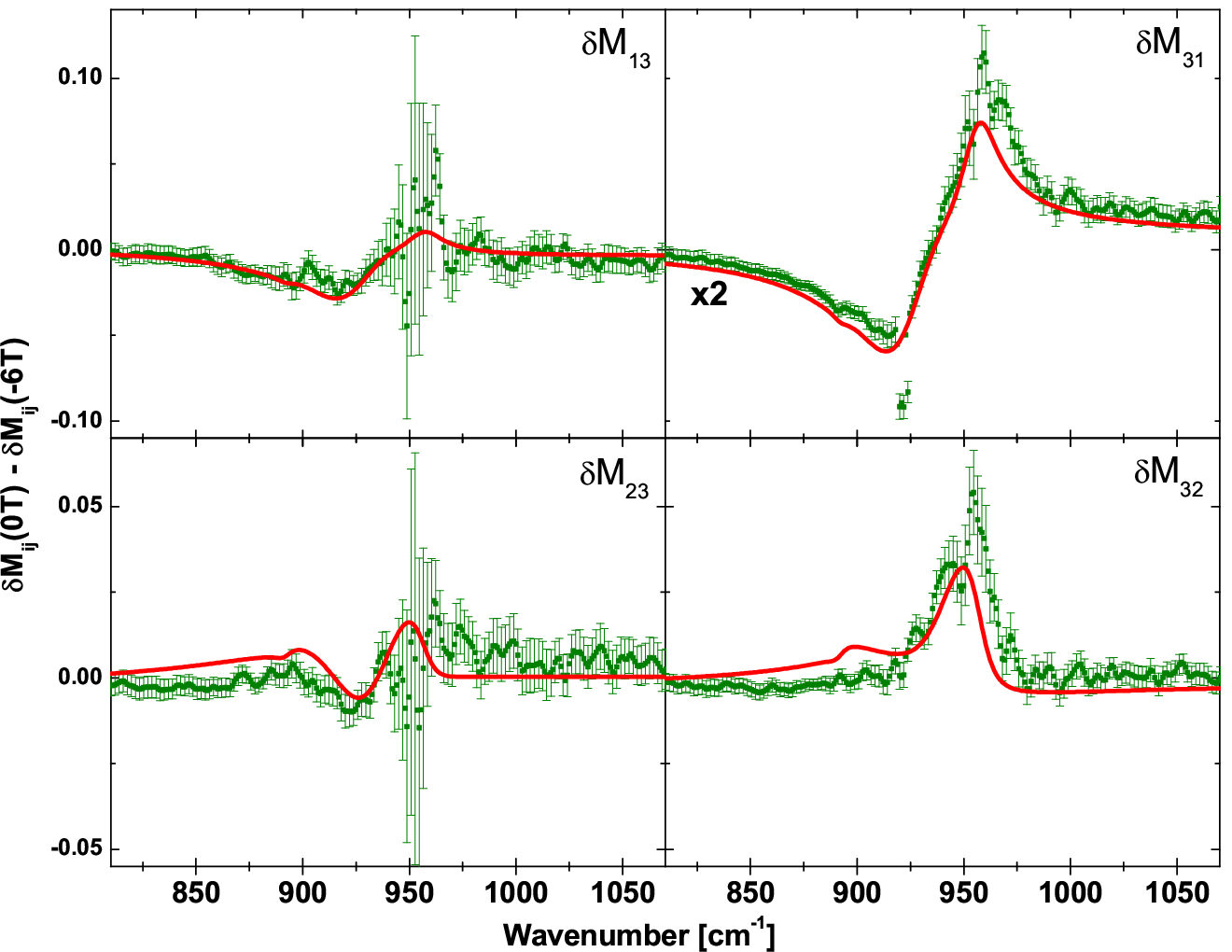
Figure 2 depicts experimental and best-match calculated OHE data in terms of Mueller matrix block off-diagonal element (Mij, ) difference data between M(0 T) and M(6 T) data sets. Note that all block off-diagonal Mueller matrix elements are zero without external magnetic field, and all differences therefrom are caused by the magnetic-field induced free charge carrier response in the InGaN layer.
| Parameter | Value | ||
|---|---|---|---|
| cm-1 | |||
| cm-1 | |||
| cm-1 | |||
| cm-1 | |||
| cm-3 | |||
| cmVs | |||
| cmVs | |||
| cm-3 | |||
| nm |
The best-match model parameters for the In0.33Ga0.67N conductive and surface depletion layers are listed in Table 1. The electron concentration in the surface depletion layer is found to be below the detection limit of the IR-VASE of 1017 cm-3. We note that a surface depletion in InxGa1-xN films should occur for In contents below (in contrast to alloys with where surface accumulation was observed), [22, 23] which is consistent with our findings. Our OHE results further revealed n-type conductivity with free electron concentration of cm-3 within the conductive In0.33Ga0.67N layer. In the OHE data analysis the effective mass and mobility parameters were allowed to have different values for polarization perpendicular , and parallel , to the -axis. A higher mobility is found along the -axis with cm2/(Vs) and cm2/(Vs). A similar anisotropy of the electron mobility parameter was also observed in GaN, InN, and AlGaN alloys and attributed to crystal domains, defect, and impurity distributions in wurtzite-structure, -plane oriented epitaxial layers.[9, 8, 14] The best-match-calculated electron effective mass parameters were determined to be and . The relative anisotropy of the electron effective mass in InN is .[8] Bearing in mind that the electron effective mass in GaN is virtually isotropic,[9] a slight anisotropy is expected for In0.33Ga0.67N. However, within our uncertainty limits, no anisotropy of the electron effective mass is detected. We note that the free electron concentration in the In0.33Ga0.67N film of 1.7 cm-3 is relatively high, which may play a role for reducing the anisotropy of the effective mass parameter. It was shown that the anisotropy of the electron effective mass parameter decreases with increasing free electron concentration in InN and vanishes for concentrations above 11019 cm-3.[8] Taking into account the error bars of the determined effective mass parameters, we estimate the highest possible relative anisotropy for In0.33Ga0.67N to be .

Figure 3 summarizes our results together with previously reported effective mass parameters for InN [8] and GaN. [9] The solid lines indicate the linear interpolation between the isotropically averaged electron effective mass parameters of GaN and InN for different electron concentrations, assuming parabolic bands in GaN and considering the nonparabolicity in InN. [24, 8] The GaN value reported by Kasic et al. [9] is considered to be independent on the electron concentration. [10] The linear interpolation for the lowest carrier concentration of cm-3 may be seen as the curvature of the conduction band bottom in InxGa1-xN. The electron effective mass parameter determined in this work is larger than the value at the bottom of the conduction band predicted by the linear interpolation. In principle, this may be due to two effects: i) a nonparabolic conduction band in In0.33Ga0.67N leading to dependence of the electron effective mass on carrier concentration, and/or ii) a nonlinear dependence with significant bowing parameter. A very small effective mass bowing parameter was theoretically predicted for InxGa1-xN.[3] We therefore compare our effective mass parameters with the linear interpolation for the electron concentration in our sample of cm-3. It can be seen from Fig. 3 that within the error bar our result is consistent with this linear interpolation, and thus indicative for nonparabolicity in In0.33Ga0.67N. A larger bowing parameter, however, cannot be ruled out. Further accurate effective mass parameters in InxGa1-xN with different electron concentrations and different In contents are needed.
In conclusion, the room temperature electron effective mass parameters perpendicular and parallel to the the -axis of In0.33Ga0.67N epitaxial layer are determined to be and for a free electron concentration of cm-3. Within our uncertainty limits, the electron effective mass parameter is found to be isotropic and the upper limit of the possible relative anisotropy is estimated to be 7%. Our results indicate that nonparabolicity of the conduction band in In0.33Ga0.67N is likely present. The free electron mobility is found to be anisotropic with cm2/(Vs) and cm2/(Vs). Our results confirm previous experimental and theoretical findings for the one mode behavior of the A1(LO) phonon and provide experimental support for the theoretical predictions of a one mode behavior of the E1(TO) phonon in InGaN.
This work was supported by the Swedish Research Council (VR) under Grant No. 2013-5580 and 2016-00889, the Swedish Governmental Agency for Innovation Systems (VINNOVA) under the VINNMER international qualification program, Grant No. 2011-03486, the Swedish Government Strategic Research Area in Materials Science on Functional Materials at Linköping University, Faculty Grant SFO Mat LiU No. 2009 00971, and the Swedish Foundation for Strategic Research (SSF), under Grant No. FL12-0181 and RIF14-055. The authors further acknowledge financial support by the University of Nebraska-Lincoln, the J. A. Woollam Co., Inc., the J. A. Woollam Foundation and the National Science Foundation (awards MRSEC DMR 1420645, CMMI 1337856 and EAR 1521428). The authors thank Dr. Mengyao Xie and Prof. Dr. Enrique Calleja (Universidad Politécnica de Madrid) for providing the In0.33Ga0.67N sample and Laurent Souqui (Linköping University) for assistance with XRD measurements.
References
- [1] J. Wu, J. Appl. Phys. 106, 011101 (2009).
- [2] L. Ardaravičius, O. Kiprijanovič, J. Liberis, E. Šermukšnis, A. Matulionis, R. A. Ferreyra, V. Avrutin, U. Özgür, and H. Morkoç, Semicond. Sci. Technol. 30, 105016 (2015).
- [3] F. Elfituri and B. Hourahine, Phys. Status Solidi A 209, 79 (2012).
- [4] M. Millot, N. Ubrig, J. M. Poumirol, I. Gherasoiu, W. Walukiewicz, S. George, O. Portugall, J. Léotin, M. Goiran, and J. M. Broto, Phys. Rev. B 83, 125204 (2011).
- [5] B. S. Yadav, P. Mohanta, R. Srinivasa, and S. Major, Thin Solid Films 555, 179 (2014).
- [6] A. Eljarrat, L. Lopez-Conesa, C. Magen, N. Garcia-Lepetit, Z. Gacevic, E. Calleja, F. Peiro, and S. Estrade, Phys. Chem. Chem. Phys. 18, 23264 (2016).
- [7] W. Walukiewicz, J. W. A. III, K. M. Yu, Z. Liliental-Weber, J. Wu, S. X. Li, R. E. Jones, and J. D. Denlinger, J. Phys. D: Appl. Phys. 39, R83 (2006).
- [8] T. Hofmann, V. Darakchieva, B. Monemar, H. Lu, W. Schaff, and M. Schubert, J. Electron. Mater. 37, 611 (2008).
- [9] A. Kasic, M. Schubert, S. Einfeldt, D. Hommel, and T. E. Tiwald, Phys. Rev. B 62, 7365 (2000).
- [10] M. Feneberg, K. Lange, C. Lidig, M. Wieneke, H. Witte, J. Bläsing, A. Dadgar, A. Krost, and R. Goldhahn, Appl. Phys. Lett. 103, 232104 (2013), http://dx.doi.org/10.1063/1.4840055.
- [11] M. Schubert, T. Hofmann, and C. M. Herzinger, J. Opt. Soc. Am. A 20, 347 (2003).
- [12] M. Schubert, P. Kühne, V. Darakchieva, and T. Hofmann, J. Opt. Soc. Am. A 33, 1553 (2016).
- [13] P. Kühne, C. M. Herzinger, M. Schubert, J. A. Woollam, and T. Hofmann, Rev. Sci. Instrum. 85, 071301 (2014).
- [14] S. Schöche, P. Kühne, T. Hofmann, M. Schubert, D. Nilsson, A. Kakanakova-Georgieva, E. Janzén, and V. Darakchieva, Appl. Phys. Lett. 103, 212107 (2013a).
- [15] M. Schubert, T. E. Tiwald, and C. M. Herzinger, Phys. Rev. B 61, 8187 (2000).
- [16] S. Hernández, R. Cuscó, D. Pastor, L. Artús, K. O’Donnell, R. Martin, I. Watson, Y. Nanishi, and E. Calleja, J. Appl. Phys. 98, 013511 (2005).
- [17] J. Ager III, W. Walukiewicz, W. Shan, K. Yu, S. Li, E. Haller, H. Lu, and W. Schaff, Phys. Rev. B 72, 155204 (2005).
- [18] H. Grille, C. Schnittler, and F. Bechstedt, Phys. Rev. B 61, 6091 (2000).
- [19] A. Kasic, M. Schubert, Y. Saito, Y. Nanishi, and G. Wagner, Phys. Rev. B 65, 115206 (2002).
- [20] S. Schöche, T. Hofmann, V. Darakchieva, N. B. Sedrine, X. Wang, A. Yoshikawa, and M. Schubert, J. Appl. Phys. 113, 013502 (2013b).
- [21] K. Torii, N. Usukura, A. Nakamura, T. Sota, S. F. Chichibu, T. Kitamura, and H. Okumura, Appl. Phys. Lett. 82, 52 (2003).
- [22] L. R. Bailey, T. D. Veal, P. King, C. F. McConville, J. Pereiro, J. Grandal, M. Sánchez-García, E. Muñoz, and E. Calleja, J. Appl. Phys. 104, 113716 (2008).
- [23] P. King, T. Veal, H. Lu, P. H. Jefferson, S. Hatfield, W. J. Schaff, and C. McConville, Phys. Status Solidi B 245, 881 (2008).
- [24] S. P. Fu and Y. F. Chen, Appl. Phys. Lett. 85, 1523 (2004).