Low-Latency Digital Signal Processing for Feedback and
Feedforward in
Quantum Computing and Communication
Abstract
Quantum computing architectures rely on classical electronics for control and readout. Employing classical electronics in a feedback loop with the quantum system allows to stabilize states, correct errors and to realize specific feedforward-based quantum computing and communication schemes such as deterministic quantum teleportation. These feedback and feedforward operations are required to be fast compared to the coherence time of the quantum system to minimize the probability of errors. We present a field programmable gate array (FPGA) based digital signal processing system capable of real-time quadrature demodulation, determination of the qubit state and generation of state-dependent feedback trigger signals. The feedback trigger is generated with a latency of with respect to the timing of the analog input signal. We characterize the performance of the system for an active qubit initialization protocol based on dispersive readout of a superconducting qubit and discuss potential applications in feedback and feedforward algorithms.
I Introduction
Recent quantum physical research is directed towards gaining experimental control of large-scale, strongly-interacting quantum systems such as trapped ions [1] and solid-state devices [2]. The ultimate goal is to realize a quantum computer [3, 4, 5, 6] with a large number of quantum bits (qubits) which may outperform classical computers for certain computational tasks [7, 8, 9, 10, 11]. However, quantum systems do not act as stand-alone components but must be combined with classical electronics to control inputs such as microwave pulses or external magnetic fields and to record and analyze the output signals [12]. Analyzing the output signals in real time can be advantageous to condition input signals on prior measurement results and therefore realize a feedback loop with the quantum system [13].
Quantum feedback schemes [14] make use of the results of quantum measurements to act back onto the quantum state of the system within its coherence time. Experimental realizations of quantum feedback have shown that it is possible to prepare and stabilize non-classical states of electromagnetic fields in optical [15, 16] and microwave [17] cavities, and to enhance the precision of phase measurements using an adaptive homodyne scheme [18].
The first demonstrations of feedback protocols with superconducting qubits showed active initialization of qubits into their ground state [19] and the stabilization of Rabi and Ramsey oscillations [20, 21]. Further recent feedback experiments with superconducting qubits demonstrated the deterministic preparation of entangled two-qubit states [22, 23], the reversal of measurement-induced dephasing [24], and the stabilization of arbitrary single-qubit states by continuously observing the spontaneous emission from a qubit [25].
Quantum feedforward schemes are closely related to quantum feedback schemes. In quantum feedforward schemes one part of a quantum system is measured while the action takes place on another part of the quantum system. A prominent example for a feedforward scheme is the quantum teleportation protocol [26], which has been realized with active feedforward in quantum optics setups [27, 28, 29, 30], in molecules using nuclear magnetic resonance [31], trapped ions [32, 33], atomic ensembles [34] and solid-state qubits [35, 36].
The feedback latency is commonly defined as the time required for a single feedback round, i.e. the time between the beginning of the measurement of the state and the completion of the feedback action onto the state. A general requirement to achieve high success probabilities in quantum feedback schemes is that the feedback latency is much shorter than the timescale on which the quantum state decoheres.
Analog feedback schemes such as those reported in Refs. [20, 25] feature feedback latencies on the order of , where the latencies are limited by analog bandwidth and delays in the cables in the cryogenic setups. However, analog signal processing circuits have limited flexibility. The flexibility can be improved by using a digital signal processing (DSP) unit in the feedback loop, which can be implemented on a central processing unit (CPU) or on a field programmable gate array (FPGA) [37]. CPU-based DSP systems offer versatile and convenient programming at the cost of several microseconds latency [17, 19] due to the delays introduced by the digital input and output of the signal, which is too slow to achieve very low error probabilities for feedback operations on superconducting qubits.
In this paper, we describe an FPGA-based feedback-capable signal analyzer which allows for real-time digital demodulation of a dispersive readout signal [38, 39, 40] and the generation of a qubit-state-dependent trigger with input–to–output latency of . Our signal analyzer is therefore among the fastest feedback-capable digital signal analyzers reported so far [41, 21, 22, 42, 43]. The capabilities of our signal analyzer enabled the feedforward action in the deterministic quantum teleportation experiment presented in Ref. [35]. In this paper, we illustrate the use of the feedback signal analyzer in a feedback loop for qubit initialization [19] and experimentally characterize its latency and performance.
The paper is organized as follows: in Sec. II we present an overview of a typical feedback loop in which our instrument is used and analyze the feedback latency. In Sec. III we discuss the implementation of the digital signal processing on the FPGA and analyze the processing latencies. Finally, in Sec. IV we experimentally characterize the performance of the feedback loop. In the appendices, we provide more details about our experimental setup and our implementation of the digital signal processing on the FPGA.
II Overview of the feedback loop
In this section, we explain the elements of a typical feedback loop shown in Fig. 1(a). We designed the feedback loop to issue pulses onto a superconducting qubit inside a dilution refrigerator conditioned on a measurement of the qubit state by analog and digital signal processing using cryogenic and room-temperature electronics. We first discuss the elements of the detection scheme and the actuator electronics and then present the latencies of the feedback loop. We provide a detailed description of our experimental setup in App. A.
II.1 Principle of the detection scheme
We consider the dispersive readout of the state of transmon qubits [44, 45] with typical frequencies for the transition between the ground and first excited state . We couple a microwave resonator to the qubit [green box in Fig. 1(a)] with a frequency difference between qubit and resonator designed to be in the dispersive regime [38, 39].
In our experimental realization of the feedback loop (see Sec. IV), the qubit transition frequency is and the center resonator frequency amounts to with dispersive coupling rate between the qubit and the resonator. Depending on whether the qubit is in state or , we observe the dispersively shifted resonator frequency at respectively.
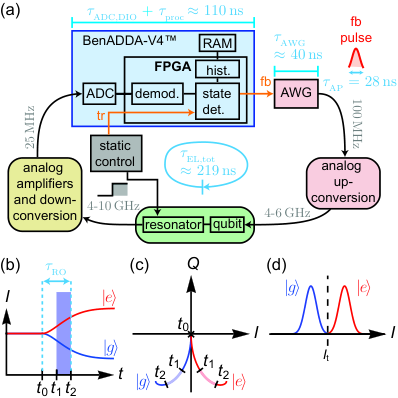
The qubit-state-dependent frequency shift leads to a state-dependent resonator response when the resonator is probed with a microwave pulse. In the dispersive readout scheme, high-fidelity quantum nondemolition readout [13] is achieved when probing the resonator with power such that the steady-state average photon number in the resonator is on the order of 1–10 microwave photons [39, 47, 48, 49, 50, 46]. Due to the low power, it is essential to connect the output of the resonator to a Josephson parametric amplifier (JPA) [51, 52, 53, 54, 47, 55, 56, 57, 58] to be able to discern the qubit-state-dependent resonator response within a single repetition of the experiment and in a time shorter than the qubit lifetime. Other schemes involve the direct coupling of a qubit to a Josephson bifurcation amplifier [59, 60, 61, 62], autoresonant oscillator [63] or parametric oscillator [64] to be able to discern the qubit state with a higher microwave power.
For simplicity, we consider the case where the resonator is probed with a microwave pulse with frequency and square envelope. The scheme considered here could be extended to include more sophisticated pulse shapes [49, 65, 66, 46] which increase the speed and fidelity of the readout as well as the speed of the reset of the intra-resonator field.
We employ the complex representation of the signal where and are the time-dependent amplitude and phase of the signal at frequency . Upon transmission of the readout pulse with frequency close to resonance, the time-dependent in-phase and quadrature components of the signal follow an exponential rise towards steady-state values starting at time after the onset of the readout pulse as illustrated in Fig. 1(b) [67]. The steady-state values depend on whether the qubit is in state (blue curve) or state (red curve). The trajectories of the readout signal in the two-dimensional plane spanned by and as sketched in Fig. 1(c) start at the center of the plane which corresponds to zero amplitude and move into two different directions depending on the qubit state (blue curve) or (red curve).
The signal is subject to noise added by passive and active components [68]. Therefore we apply a linear filter to the signal with the goal to attenuate noise frequency components while keeping the frequency components that contain the signal [40, 24, 69, 46]. In particular, we apply a moving average filter which is advantageous in terms of the signal processing latency (see Sec. III.3). The moving average is equivalent to an unweighted integration of the original signal in a particular integration window starting at a variable time and ending at time [see Fig. 1(b) and Fig. 1(c)], where is a constant integration time. We define the total readout duration as the time difference between the onset of the readout pulse and the end of the integration window. In the experiment presented in Sec. IV we used an integration window of and a readout duration of .
In the absence of transitions between qubit states during the integration time, the statistical distribution of the integrated signal, when the experiment is repeated many times, is expected to be represented by two Gaussian-shaped peaks in a histogram of the component [Fig. 1(d)]. In the presence of qubit state transitions during the readout, the distributions corresponding to the states and are expected to be non-Gaussian with an increased overlap [40, 46]. We discern the states and of the qubit by comparing the signal to a threshold value [dashed line in Fig. 1(d)]. The fidelity of the readout depends on the signal–to–noise ratio of the readout signal [49, 46]. To maximize the readout fidelity, we optimize the integration window and threshold value .
II.2 Implementation of the detection scheme
The readout pulse is issued by the static control hardware [gray box in Fig. 1(a)]. Simultaneously, the static control hardware sends a trigger [ in Fig. 1(a)] to the FPGA to synchronize the digital signal processing with the readout pulse.
We use an analog detection chain [yellow box in Fig. 1(a)] containing amplifiers with a total gain of approximately (see App. A) to detect the signal at the output of the resonator. In addition, the detection chain uses analog down–conversion electronics to convert the readout signal to an intermediate frequency compatible with the sampling rate of our DSP unit. We choose an intermediate frequency at a quarter of the sampling frequency, i.e. , which allows for efficient digital down–conversion (see Sec. III.3). Note that in principle it is possible to directly demodulate the signal into its and components in the analog signal processing but this requires the and component of the signal to be digitized using two separate analog-to-digital converter (ADC) channels [70, 41, 71]. The separate digitization of the and components is sensitive to mismatches between the conversion-loss and reference level which lead to a distortion of the digitized complex signal. In contrast, down–conversion to an intermediate frequency in the range of to avoids low-frequency noise, DC offsets and requires only one ADC channel at the cost of a reduced bandwidth [70, 41, 71].
We implement the digital signal processing on a Xilinx Virtex–4 FPGA mounted on a commercial DSP unit by Nallatech, Inc. (BenADDA-V4™) [blue box in Fig. 1(a)] which includes an ADC with sampling rate and 14-bit voltage resolution. In a first step, the DSP digitally demodulates the signal [labeled as demod. in Fig. 1(a)]. The state discrimination module [state det. in Fig. 1(a)] then compares the filtered signal at time to the threshold , to determine the qubit state from the demodulated signal. Depending on the determined qubit state, a feedback trigger [ in Fig. 1(a)] is sent from the FPGA to the actuator electronics.
II.3 Actuator
The actuator is realized with an arbitrary waveform generator (AWG). When it receives the feedback trigger, the AWG generates a feedback pulse with a sampling rate of . In our experiment, the actuator pulse (AP) has a duration of and uses the derivative removal by adiabatic gate (DRAG) technique [72, 73] to prevent transitions to higher-excited states of the transmon outside of the subspace spanned by the states and . We typically generate the actuator pulse with a carrier frequency of limited by the bandwidth of the AWG and analog mixer. In the experiment presented in Sec. IV we chose a carrier frequency of for the actuator pulse. We use an analog mixer to up–convert the actuator pulse to the qubit transition frequency, which is typically in the range of . Forwarding this pulse to the qubit realizes a conditional quantum gate on the qubit closing the feedback loop.
II.4 Latencies
We define the latency of the feedback loop [Fig. 1(a)] as the time from the beginning of the readout pulse until the completion of the feedback pulse, i.e.
| (1) |
where is the total electronic delay of the signal in the analog and digital components and cables of the feedback loop, the readout duration (see Sec. II.1) and is the length of the actuator pulse (see Sec. II.3). We measured the total electronic delay in-situ by changing the up–conversion frequency of the feedback pulse to the resonance frequency of the readout resonator and adjusting the amplitude of the pulse. The resonant feedback pulse is transmitted through the resonator which makes it possible to determine the timing of the feedback pulse relative to the readout pulse. By adding up the contributions according to Eq. (1) we infer a feedback latency of .
The electronic delay
| (2) |
can be broken up into accumulated contributions. The signal processing, which we implemented in the FPGA, introduces a processing delay of three clock cycles (see Sec. III). The feedback trigger is delayed by with respect to the analog input signal, where is the delay introduced by the ADC and digital interfaces (see App. B).
By subtracting the separately determined quantities , and from the total electronic delay we estimate the inferred total group delay in the cables and analog components. We expect the total cable length connecting the analog and digital components to be the dominant contribution to the inferred group delay. The inferred group delay corresponds to an approximate total cable length of considering an effective dielectric constant for the coaxial cables with PTFE dielectric. This inferred total cable length is consistent with the experimental setup. The cable length in our setup could be reduced further by placing the individual components of the feedback loop closer to each other which can be achieved, for example, by placing the FPGA and control electronics inside the dilution refrigerator [74, 75, 76].
III FPGA-based digital signal processing
In this section, we describe our digital signal processing (DSP) circuit which we implemented on the Virtex–4 FPGA. To derive feedback triggers, the DSP circuit (Fig. 2) determines the qubit state by digital demodulation of the readout signal (see Sec. II). We start by discussing the digitization and synchronization of the input signal. Next, we discuss the signal processing features of each block and the corresponding latencies. Details of the FPGA implementation of each signal processing block are discussed in App. C. We analyze the FPGA timing and resource usage for the implementation of the DSP circuit on the Xilinx Virtex–4, Virtex–6 and Virtex–7 FPGA in App. D.
III.1 Digitization of the input signal
Before entering the DSP circuit, the readout signal is digitized by an external ADC chip which samples the signal with rate . Typical readout signals are sine waves with qubit-state-dependent amplitude and phase as shown in Fig. 3(a). We parameterize the time-dependent voltage at the input of the ADC as
| (3) |
As discussed in Sec. II.2, we choose an intermediate frequency of for the readout signal after analog down–conversion (see Sec. II.2) which is a useful choice for digital demodulation as discussed below. The time-dependent amplitude is proportional to the amplitude of the field at the output of the resonator scaled by the gain of the analog detection chain and conversion loss of the mixer.
The ADC samples the signal at discrete times with index . The ADC encodes the input voltage range of approximately as 14-bit fixed-point binary values. The fixed-point representation leads to a discretization step size of . A trigger pulse () is provided together with the analog signal via a separate digital input of the FPGA to mark the onset of the readout pulse.
III.2 Pipelined processing
We designed the DSP circuit to process the signal from the ADC in a pipelined manner. The signal from the ADC is initially buffered in a register implemented by synchronous D–flip–flops (ADC block in Fig. 2) which forward the value of the signal at each event of a rising edge of the sampling clock to the next processing element in the pipeline.
A separate trigger input (, orange lines in Fig. 2) marks the beginning of each experimental repetition. In order to synchronize the trigger with the ADC signal, the trigger initially goes through six pipelined registers ( in Fig. 2), which compensate the difference in delay between the ADC line and trigger line. To synchronize the signal processing with the sampling clock, we insert further pipelined registers into the signal and trigger lines at specific points in the circuit (blue dashed lines in Fig. 2).

III.3 Digital demodulation
As discussed in Sec. II.2, we digitally demodulate the readout signal to obtain the and components of the signal. Digital demodulation is achieved by digital frequency down–conversion which involves digital mixing of the signal with a digital reference oscillator followed by digital low–pass filtering to remove noise and unwanted sideband frequency components [71].
III.3.1 Digital mixing
In the first part of the digital demodulation circuit (yellow box in Fig. 2), we implement a digital mixing method [70, 71] (digital mixer in Fig. 2) to obtain a sideband at zero frequency. In the digital mixer, the input signal as defined in Eq. (3), is multiplied with a complex exponential with down–conversion frequency to obtain a complex output signal ,
| (4) |
The action of the multiplication is to generate two sidebands corresponding to the two complex exponentials in Eq. (4); one is corresponding to the complex signal and the other leads to oscillations with frequency of the output signals of the mixer [Fig. 3(b)]. The complex signal is the basis on which we determine the state of the qubit after filtering out the oscillating sideband (see following sections).
In practice, the real () and imaginary () parts of the output signal of the mixer are computed separately by multiplying the input signal with a discrete cosine to obtain the real part and with a discrete negative sine to obtain the imaginary part. The FPGA implementation of the digital mixer is described in App. C.1. For , the digital mixer introduces a latency of less than one clock cycle () due to its multiplier-less implementation [70, 71]. Since the output signal of the mixer is registered by synchronous D–flip–flops, the effective latency is one clock cycle. For synchronization, the trigger signal () is delayed by one clock cycle [ in Fig. 3(b)].
III.3.2 Digital low-pass filter
The second essential part of the digital down–conversion circuit is a digital low-pass filter, which extracts the and components from the signals and by removing the sideband spectral components oscillating at frequency [71]. We implement the digital low-pass filter as a finite impulse response (FIR) filter [71] which is a discrete convolution of the digital signal with a finite sequence of filter coefficients. By matching the filter coefficients (integration weights) to the expected resonator response, it is possible to optimize the single-shot readout fidelity [40, 48, 49, 24, 69, 46]. While our DSP circuit in principle allows for 40-point FIR filters with arbitrary filter coefficients, a moving average is the simplest type of FIR low-pass filter which is possible to implement without multipliers and therefore has a reduced processing latency and uses less FPGA resources than a more general FIR filter. The FPGA implementation of the moving average module is described in App. C.2.
The moving average (FIR filter in Fig. 2) is applied separately to the real part () and imaginary part () of the complex output signal of the digital mixer, , leading to
| (5) |
which is a discrete convolution with a square window of length . In the limit of negligible modulation bandwidth, the moving average filters a sinusoidal perfectly if the window length is a multiple of the oscillation period. In the case of , the periodicity of the unwanted terms at is equal to two discrete samples. Therefore any window length which spans an even number of samples is suitable to filter out the sideband.
The output of the moving average with window length is shown in Fig. 3(c). The and signals at the output of the moving average show a smooth ramp towards a steady-state value. In the simulated signals shown in Fig. 3 an appropriate global phase offset has been chosen such that the difference between the traces corresponding to the and state is maximized in the component of the signal (see Sec. II.1).
The moving average module has a latency of one clock cycle. The trigger is delayed accordingly by one additional clock cycle () for synchronization.
III.4 Offset subtraction and scaling
Following the FIR filter block, the and signals enter blocks which perform offset subtraction and scaling of the signal (green boxes in Fig. 2). The main purpose of offset subtraction is to set a threshold value as described in Sec. III.5. Moreover, offset subtraction and scaling allows to make best use of the fixed range and resolution used for recording histograms (see Sec. III.6).
The outputs of the offset subtraction and scaling blocks are described by
| (6) | ||||
| (7) |
where and are offsets in the I/Q plane and and are multiplication factors. We determine the parameters and in a calibration measurement. The latencies of the offset subtraction and scaling blocks are less than one clock cycle and no synchronous D–flip–flops are used.
III.5 State discrimination module
The state discrimination module (red box in Fig. 2) determines the state of the qubit based on the preprocessed input signals and . Due to the offset subtraction, the threshold value for state discrimination can be kept fixed at zero which simplifies the FPGA implementation of the state discrimination module as discussed in App. C.4.
The readout time relative to the onset of the readout pulse (see Sec. II.1) is specified with a variable delay of clock cycles after the detection of the trigger signal, i.e. . In the example shown in Fig. 3(c), the and states of the qubit are discriminated based on a threshold value (thick horizontal bar) defined for the signal at a time which is clock cycles after the detection of the trigger signal . The simulated signals corresponding to the [blue curve in Fig. 3(c)] and [red curve in Fig. 3(c)] state are well distinguishable at the time when the threshold is checked, such that the state of the qubit can be determined successfully even in presence of noise (see Sec. IV). The state discrimination module either issues the feedback trigger [red curve in Fig. 3(d)] or does not issue the feedback trigger [blue curve in Fig. 3(d)] based on the determined qubit state.
Our DSP circuit provides the possibility to derive a second feedback trigger ( in Fig. 2) based on both the in-phase () or quadrature () signal components. For example, in the quantum teleportation protocol [26] the states of two qubits at the sender’s location are measured in order to perform a state-dependent rotation on a qubit at the receiver’s location. In our experimental realization of the teleportation protocol as discussed in Ref. [35], we discriminated the states of the two sender’s qubits based on two threshold values defined for the and signals. Based on the outcome of comparing the and signals to the two threshold values, we issued two independent trigger signals to two separate AWGs in order to implement a conditional operation on the receiver’s qubit [35].
III.6 Histogram module
The histogram module records how often the values of the signals and obtained from a specific integration window fall into a particular histogram bin when the experiment is repeated many times. The bins are defined by subdividing the signal range from -1 to +1 into typically 128 bins. From the histogram, an estimate of the probability density function of the signal at the specified times is obtained.
We typically repeat the experiment – times to obtain standard deviations of less than a part per thousand for the counts in each histogram bin. Storing the histogram of the signal needs less memory than storing the value of the signal in each repetition if the number of repetitions exceeds the number of histogram bins. The histogram module therefore allows for data reduction at the time when the data is recorded.
We have used the histogram module in previous experiments to characterize the quantum statistics of microwave radiation emitted from circuit QED systems [77, 78, 79, 80]. In the context of feedback experiments, we record histograms to obtain the probabilities of observing a particular qubit state in two consecutive qubit readouts as described in Sec. IV.
We update the histogram at the same time as the state discrimination module determines the qubit state in order to analyze the readout fidelity and feedback performance (see Sec. IV). We synchronize the state discrimination module and the histogram module using a marker signal ( in Fig. 2) which is sent from the state discrimination module to the histogram module. We use an external Zero Bus Turnaround (ZBT) Random Access Memory (RAM) (see Fig. 2) to store the histogram. When the recording of the histogram is completed, we transfer the histogram to the host computer via the interface. The implementation details of the histogram module are described in App. C.5.
IV Qubit state initialization experiment
In this section, the functionality of the presented DSP circuit is demonstrated in the context of a qubit state initialization experiment. In the experiment we use the feedback loop to reset the state of a superconducting qubit [81, 82, 19, 83] (see App. E) deterministically into its ground state, independent of its initial state. We correlate the outcomes of two consecutive qubit measurements in order to separate out the different effects such as the qubit lifetime and readout fidelity which contribute to the overall performance of the feedback protocol.
We choose the repetition period of the experiment to be longer than the qubit lifetime , such that the qubit is approximately in thermal equilibrium with its environment at the beginning of each experimental repetition. We observe a finite thermal population of the excited state due to the elevated effective temperature of about of the system on which the experiments were performed (see App. F).
In order to test the feedback protocol, we prepare an equal superposition of the computational states and of the superconducting qubit. This choice of initial state will ideally lead to equal probabilities to find the states and when the qubit is measured. Preparing an equal superposition as an initial state will therefore test the feedback actuator for both computational states and of the qubit. An additional data set (App. F) shows that the feedback scheme can also be used to reduce the thermal population of the excited state [84, 82, 19], providing an additional benchmark for our feedback loop.
Ideally, we consider the case when the qubit is initialized in the state corresponding to the Bloch vector pointing to the upper pole of the Bloch sphere [stage 1 in Fig. 4(a)]. A microwave pulse at frequency [green line in Fig. 4(b)] is applied to the qubit to realize a rotation which brings the qubit into the superposition state corresponding to a Bloch vector pointing at the equator of the Bloch sphere [stage 2 in Fig. 4(a)].

When the qubit initially is in state , for example due to the non-zero temperature of the system, the effect of the rotation is to prepare the state which is an equal superposition of and with a different phase. The states and are expected to lead to an identical distribution of outcomes in the state detection.
In the experiment, directly after the preparation of the initial state, at time , the state of the qubit is measured with a readout pulse of length (see in Fig. 4) applied to the resonator. The dispersive readout projects the state of the qubit into either the ground or excited state corresponding to the upper and lower pole of the Bloch sphere [stage 3 in Fig. 4(a)]. The DSP (see Sec. III) extracts the in-phase component during the readout pulse . We filter the signal with a moving average of four consecutive samples, corresponding to an integration window [blue region M1 in Fig. 4(b)] of . We extracted the time of the end of the integration window 11 1 It is in principle possible to shorten the duration of the readout pulse to match the end of the integration window at but we keep the length of the readout pulse constant to simplify the calibration procedure. relative to the beginning of the readout pulse by fitting a theoretical model to the switch-on dynamics of the readout signal in a time-resolved measurement [46].
The histogram of [blue dots in Fig. 4(c)] reveals two Gaussian peaks corresponding to the distributions of the in-phase signal for the qubit being in state or . The measured initial excited state probability , is the fraction of counts of values above the threshold value [dashed line in Fig. 4(c)] relative to the total count of measurements.
With a master equation [86] we simulate the decay of the qubit state with characteristic time during the time of the pulse and the readout up to the center of the integration window [see Fig. 4(b)]. Furthermore we take into account a bias of the measured probabilities towards due to the finite readout error of (see App. G). From the master equation simulation we obtain an expected excited state probability of in the first measurement which agrees reasonably with the measured probability (see above). A source of systematic errors is measurement-induced mixing [87]. An additional reason for the systematic deviation of the measured probability from the simulated probability is that the chosen threshold value deviates from the value which optimizes readout fidelity (see App. G). This offset leads to a bias of the observed probabilities towards the ground state in addition to a systematic bias due to state transitions during the integration time [46].
The feedback loop is configured to deterministically prepare the state [stage 4 in Fig. 4(a)]. The feedback pulse, inducing a rotation of the Bloch vector of the qubit, turns the state into and vice versa. Thus, the feedback pulse is issued only if the first measurement revealed the qubit to be in state . The pulse [red dashed line in Fig. 4(b)] arrives at the qubit with delay of (see Sec. II.4) conditioned on the readout result of .
For verification, a second readout pulse ( in Fig. 4) is applied to the qubit at the time directly after the arrival of the feedback pulse at the qubit. The difference between and the beginning of the first readout pulse corresponds to the total feedback latency (see Sec. II.4). We recorded histograms of , which is the filtered in-phase component of the signal at time . When the feedback actuator is disabled, the histogram of [orange dots in Fig. 4(c)] shows reduced counts on the right side of the threshold with an excited state probability of . Extending the master equation simulation introduced above to include the full pulse sequence up to the second readout pulse, we obtain in reasonably good agreement with the measured value. The state decay between and , which leads to the observed reduction in the excited state population, causes errors in the feedback action as discussed below.
When the experiment is repeated with the feedback actuator enabled, the double-peaked histogram obtained from the first readout [blue dots in Fig. 4(d)] is approximately identical to the case without feedback, as expected, with the measured excited state probability agreeing with within the statistical error bars. After the feedback pulse, in the histogram of [orange dots in Fig. 4(d)], the measured excited state probability is significantly reduced to . This probability compares reasonably well with the simulated value of obtained from the master equation simulation introduced above. We attribute the difference between the measured and simulated value of to measurement-induced mixing and the deviation of the feedback threshold from the optimal value (see above).
To obtain a figure of merit for the feedback protocol that is independent of characteristics such as state decay and temperature of the quantum system, we study correlations between the outcomes of the two readout pulses and . From the two-dimensional histograms [Fig. 4(e,f)] with axes and , we obtain experimental probabilities to observe a specific range of two consecutive measurement outcomes . The probabilities correspond to observing the qubit in state with the first readout pulse and consecutively in state with the second readout pulse. These probabilities are obtained from the normalized counts in the four quadrants (, , , ) separated by the threshold [dashed lines in Fig. 4(e,f)].
When the feedback is enabled, the measured probability [Fig. 4(f)] corresponds to the unwanted event of the state being observed consecutively with both readout pulses. We explain the dominant contribution to by state decay between the first readout pulse and the feedback pulse. The probability of state decay between the first and second readout pulse is extracted from a reference measurement of [Fig. 4(e)] when the feedback is disabled. The probabilities and are close to each other since the conditional pulse swaps the state with before the second readout pulse. The corresponding simulated probabilities and (see Tab. 1) are in reasonable agreement with the experimental values considering the sources of systematic errors as discussed above.
The measured probability [Fig. 4(f)] of a transition from state to when the feedback loop is enabled is close to the reference value [Fig. 4(e)] when the feedback is disabled. This shows that the state is correctly left unchanged when the qubit is already in state . A possible reason for the small systematic deviation of from , which is on the order of , could be drifts in the experimental parameters such as the phase of the readout signal.
In summary, the probabilities of the combined events (Tab. 1) show that in the feedback protocol the pulse is applied only when it is intended and that the probability of the unwanted events in region is limited by state decay between the first measurement and the feedback pulse.
| feedback off | feedback on | |||
|---|---|---|---|---|
| exp. | sim. | exp. | sim. | |
| 52.06(3)% | 50.74% | 52.32(3)% | 50.74% | |
| 1.88(1)% | 2.18% | 1.67(1)% | 2.18% | |
| 12.97(2)% | 11.37% | 34.45(3)% | 38.75% | |
| 33.10(3)% | 35.71% | 11.57(2)% | 8.32% | |
V Conclusions and discussion
We developed a low-latency FPGA-based digital signal processing unit for quantum feedback and feedforward applications such as the qubit initialization scheme presented in this paper and the deterministic quantum teleportation realized in Ref. [35].
Our experimental results show that the feedback loop performs as expected. The total feedback latency amounts to determined by the sum of ADC latency, processing latency, AWG latency, cable delays, readout time and feedback pulse duration. To reduce the probability of state decay between the state detection and the feedback action, the ratio of the feedback latency to the qubit lifetime needs to be reduced. Since the probability of state decay is expected to be proportional to , a time of about would be needed to achieve error probabilities of less than in one iteration of the feedback scheme presented in this work. Conversely, with the longest times achievable with state-of-the art superconducting circuits of up to approximately [88, 89, 90], feedback latencies of less than would be needed to reduce the error probability to less than one part per thousand. In the present work, we demonstrated digital processing latencies on the order of , which are among the shortest latencies reported for FPGA-based signal analyzers [21, 22, 43] in the context of superconducting qubits. Simultaneously, the usage of advanced readout strategies enables a shorter optimal readout times [49, 46]. Shorter latencies for analog–to–digital conversion and cable delays may be achievable by using custom-made circuit boards which work at cryogenic temperatures [74, 75, 76] or by on-chip logical elements [91, 92, 93].
Low latency feedback loops may play a role in realizing future quantum computers, where a key ingredient is quantum error correction [94, 95, 96] in which error syndromes of a quantum error correction code are detected by repetitive measurements. The syndrome measurements are designed to keep track of unwanted bit flip and phase errors. In this context it is essential to have a flexible low latency classical processing unit to process the error syndromes without causing additional delay for the quantum processor. A large set of quantum error correction codes may work with a passive ‘Pauli frame’ update [97], however, it still remains an open question [98] whether some level of correction and qubit reset using active feedback is preferable. Therefore, having a low latency signal processor with feedback capabilities as presented in this work, will be instrumental for scaling up quantum technologies.
Acknowledgements.
The authors would like to thank Deniz Bozyigit for initial contributions to the FPGA firmware. The authors further acknowledge useful discussions with Johannes Heinsoo, Sebastian Krinner, Markus Oppliger and Lars Steffen. The authors acknowledge financial support by the National Centre of Competence in Research Quantum Science and Technology (NCCR QSIT), a research instrument of the Swiss National Science Foundation (SNSF), by the Swiss Federal Department of Economic Affairs, Education and Research through the Commission for Technology and Innovation (CTI), by the Office of the Director of National Intelligence (ODNI), Intelligence Advanced Research Projects Activity (IARPA), via the U.S. Army Research Office grant W911NF-16-1-0071 and by ETH Zurich. The views and conclusions contained herein are those of the authors and should not be interpreted as necessarily representing the official policies or endorsements, either expressed or implied, of the ODNI, IARPA, or the U.S. Government. The U.S. Government is authorized to reproduce and distribute reprints for Governmental purposes notwithstanding any copyright annotation thereon.Appendix A Experimental setup
The device under test (DUT, green box in Fig. 5) is a superconducting circuit with one superconducting transmon qubit. The DUT is thermalized to the stage of a dilution refrigerator (purple box in Fig. 5).

Single-qubit quantum gates are realized by driving transitions between the ground and first excited state of the transmon by applying microwave pulses through a dedicated microwave line (port A in Fig. 5). The microwave line is thermalized by attenuators at three temperature stages . The attenuators reduce the signal and noise coming from the room-temperature electronics and add Johnson-Nyquist noise at their respective temperature , thereby reducing the effective temperature of the microwave radiation in the cable. The qubit pulses for static control (grey box in Fig. 5) are generated by AWG 1 and up–converted to microwave frequencies using an I/Q mixer driven by a local oscillator (LO) signal from microwave generator MWG 1.
Readout of the qubit is realized by a pulsed measurement of the transmission of microwaves through a coplanar waveguide resonator (CPWR). The readout pulse is applied to the CPWR through the resonator drive line (port B in Fig. 5). The readout pulses are also generated by AWG 1. An I/Q mixer with an LO signal from MWG 2 allows for shaping the readout pulses which can be useful to achieve faster ring-up and ring-down of the intra-cavity field [66, 65]. In order to adjust the power range for the resonator drive a variable attenuator is used at the RF output of the mixer.
The transmitted signal is directed through an isolator, circulator, and directional coupler to a Josephson parametric amplifier (JPA) [51] based on a resonator shunted with an array of SQUID loops [52, 53, 56]. The isolators and circulators protect the DUT from pump leakage and thermal noise. The pump tone needed to achieve a gain of approximately in the JPA is derived via splitters from the same microwave generator MWG 2 as is used for the readout pulses which reduces drifts of relative phase between the two signals. Low phase noise is essential if the JPA is operated in a phase-sensitive mode [99, 80]. The pump signal (port E in Fig. 5) is combined with the signal from the resonator through a directional coupler.
Both the signal and pump tone are reflected from the JPA. To avoid saturation of the subsequent amplifiers, we destructively interfere the reflected pump tone with a cancellation tone applied to the directional coupler (port D in Fig. 5). The phase and amplitude of the cancellation tone are adjusted using a variable phase shifter and attenuator.
After amplification by the JPA, the signal is passed via isolators which attenuate reversely propagating radiation towards a high-electron-mobility transistor (HEMT) amplifier to further amplify the signal with a gain of before it exits the dilution refrigerator (port C in Fig. 5).
In the detection electronics (yellow box in Fig. 5) at room temperature, the signal is amplified further using low-noise microwave amplifiers. In order to reduce noise below the frequencies of interest, the signal is high-pass filtered with a cut-off frequency of about . The carrier frequency of typically is converted down to an intermediate frequency (IF) using an analog I/Q mixer and a separate microwave generator, MWG 3, for the LO signal. The IF signal at the output of the mixer is further amplified using an IF amplifier and low-pass filters are used to suppress noise outside the detection bandwidth of the ADC (). Attenuators between the amplifiers and the mixer are used to suppress standing waves due to impedance mismatches and in order to prevent saturation of the mixer, amplifiers and ADC.
After amplification and analog down–conversion, the signal is digitized by the ADC and forwarded to the FPGA on the Nallatech BenADDA-V4™card. The digital signal processing (DSP) circuit which we implemented on the FPGA generates a feedback trigger conditioned on the digitized and processed signal (see Sec. III).
The feedback trigger is forwarded to AWG 2 which is part of the actuator electronics (red box in Fig. 5). When receiving the feedback trigger, AWG 2 generates a pulse which is up–converted to the qubit frequency, typically at –, using an I/Q mixer and LO from microwave generator MWG 4. Bias–tees allow to compensate unwanted DC offsets of the I/Q inputs of the mixer in order to suppress LO leakage. The up–converted microwave pulses are forwarded to the qubit (port A in Fig. 5).
All AWGs, MWGs, as well as ADC and DSP clocks are synchronized to a sine wave from an SRS FS725 rubidium frequency standard.
Appendix B Latency of analog to digital conversion and digital input
The ADC latency and digital input–output latencies of the FPGA are inferred from the timing relative to the input trigger and feedback trigger. When the variable delay in the state discrimination module (see App. C.4) is set to clock cycle, we measure the delay from the trigger input to the feedback trigger with an oscilloscope to be . Since the input trigger is synchronized with the digitized signal from the ADC in the DSP circuit, we infer that the ADC delay and digital input–output delay is .
The delay has several contributions which we did not determine individually. The pipelined architecture of the AD6645 ADC introduces a delay of four clock cycles () and a latency of one additional clock cycle () to transfer the digitized signal from the ADC to the FPGA where it is registered in a synchronous D–flip–flop. Further delays are expected to contribute to due to the routing of the digital signal on the BenADDA-V4™board as well as pad–to–flip–flop and flip–flop–to–pad delays on the FPGA (see App. D.1).
Appendix C Implementation details of digital signal processing blocks
Here we specify implementation details of the blocks of the DSP circuit presented in Sec. III which are relevant for the processing latency.
C.1 Digital mixer
The cosine and sine signals, and , for digital mixing are typically generated either using a lookup table with precomputed values or by an iterative algorithm and then multiplied with two copies of the signal as shown in Fig. 6(a). While these methods work for arbitrary frequencies , a simplified method exists for the special case when equals a quarter of the sampling rate, i.e. [70, 71].

In the case, the periodic sequences for the cosine and negative sine are simply and respectively [70]. Since multiplication with , and is trivial, we replace the multipliers by counter-driven multiplexers (MUX) that periodically switch between four inputs as shown in Fig. 6(b). The 2-bit repeating counter (CNT) iterates through a sequence of four values , jumping to the next value in every clock cycle and restarting from after it has reached . The output of the counter is forwarded to the selection (sel) input of the multiplexers (MUX). The selection input of the multiplexers determine which of the four inputs of the multiplexers are forwarded to their output. The four inputs of the multiplexer for the real part (), correspond to multiplying the signal with while the inputs of the multiplexer for the imaginary part () correspond to multiplication with .
C.2 Moving average
In the following, we discuss how to implement the moving average (circuit shown in Fig. 6(c)), which is the simplest type of FIR filter, with a processing latency of less than one clock cycle (). The moving average is applied in parallel to the real and imaginary parts of the output of the mixer, i.e. two copies of the circuit shown in Fig. 6(c) are implemented with outputs and respectively.
The first step in the circuit for computing the moving average, as shown in Fig. 6(c), is to fan out the input signal into two branches. One branch is delayed by a variable delay () of clock cycles while no operation is performed on the other branch , i.e. . A subtractor then computes the difference between the values of the two branches which is forwarded to an accumulator [+= in Fig. 6(c)]. In every clock cycle, the accumulator adds the value at its input to the sum stored internally and forwards the updated sum to the output. Therefore the output at clock cycle of the accumulator is the sum of all input samples up to clock cycle , i.e.
| (8) |
where the last equality holds assuming that all input samples with negative index are equal to zero, i.e for . To make sure that this assumption holds true, we initialize the registers of the variable delay and the accumulator to zero. As depicted in Fig. 6(c), an additional adder (+) adds the most recent value of the difference at the input of the accumulator to its output and a constant factor of normalizes the moving average. Thus, the final signal at the output of the moving average module () is
| (9) |
As opposed to the sums in Eq. (8), which stop at index , the final sum in Eq. (9) includes the most recent sample with index , which shows that the additional adder reduces the effective processing latency to less than one clock cycle.
C.3 Preprocessing module
Offset subtraction ( in Fig. 6(d)) is implemented with lookup tables (LUTs). The parameter is configurable via the interface with the host computer (indicated by dashed arrows). The multiplication ( in Fig. 6(d)) is implemented without the use of actual multipliers but rather uses bit shift operations, which are effective multiplications with powers of two. Avoiding the allocation of multipliers reduces hardware resource consumption and leads to reduced processing latencies. The multiplication is made configurable using multiplexers to choose between different bit shift operations. The bit shift operation is chosen via the host computer interface.
C.4 State discrimination module
The state discrimination module determines the qubit state and provides feedback triggers based on the sign bits and of the preprocessed signals and as shown in Fig. 6(e). The sign bits of and are if the respective signal is positive and if it is negative, as depicted in Fig. 6(f). Due to the prior offset subtraction, determining the sign bits of and is equivalent to comparing the and signals each to an arbitrary threshold value. Two lookup tables (LUT) define the binary feedback with two independent bits and which are selected based on the two sign bits and as depicted in Fig. 6(g). The entries of the LUT can be set via the host computer interface [dashed arrows in Fig. 6(e)]. In the example shown in Fig. 6(h), the value of the feedback bit is if and only if corresponding to a non-negative value of the component of the signal.
The input trigger signal is used as a reference for the timing of the feedback triggers relative to the onset of the readout pulse. As shown in Fig. 6(e), the trigger first enters a rising edge detection block. The output of the rising edge detection block is if and only if the input binary value of the trigger was in the previous clock cycle and in the present clock cycle. The output of the rising edge detection is delayed with a variable delay where is the number of clock cycles (each being ) corresponding to the readout time , i.e. . The parameter can be set via the host computer interface. The output of the variable delay, to which we refer as the marker, marks the specific time at which the feedback pulse is provided. To assert that the feedback triggers are issued at the correct time, the feedback triggers and are based on the AND operation of the output of the LUT and the marker.
C.5 Histogram module
The histogram module is important to assess the feedback performance and to calibrate the experimental setup. Here we explain how our multi-dimensional histogram module is implemented. The histogram module has different operational modes. We first introduce the circuit for recording two-dimensional histograms as shown in Fig. 7(a). The input signals and are rounded to 7-bit fixed point numbers which means that the full range of is subdivided into bins. The 7-bit fixed-point representations of and are concatenated into a 14-bit address of the histogram bin which stores the number of occurrences of the combination of values . The “increase count” block manages the communication with the ZBT RAM in order to increase the stored count whenever the enable flag (en) is active. For feedback experiments, the enable flag is derived from the marker such that the histogram is updated when the feedback decision is made (see Sec. III).
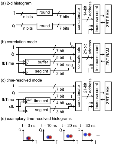
In the correlation mode of our histogram module, a buffer [Fig. 7(b)] stores the value of at every reception of the marker. The buffered signal is combined with the most recent signal to record the probability to observe a specific combination and in two consecutive readouts (see Sec. IV). In addition a segment counter [seg cnt in Fig. 7(b)] allows to distinguish alternating experimental scenarios, such as when the feedback is enabled or disabled alternately in consecutive runs of the experiment. In the correlation mode, the value of is in principle not needed but is an additional useful piece of information. In order to make use of the total amount of bits (4 MB) available space in the ZBT RAM, we reduce the Q dimension to 5 bits and concatenate the values (, , , seg) into a 21-bit address with a word size of 16 bits to store the counts as presented in Fig. 7(b).
In the time-resolved mode, a time counter [time cnt in Fig. 7(c)] is used to add time as an additional dimension of the histogram. The time counter starts upon the reception of the marker and the enable flag is held active for up to 16 clock cycles. As for the correlation mode there is a segment counter [seg cnt in Fig. 7(c)] which allows to discern different consecutive scenarios such as when the qubit is prepared in the or state alternately. This makes the time-resolved mode useful for calibration tasks such as finding the optimal qubit readout time by observing the separation of the distributions of and values for the states [blue histogram in Fig. 7(d)] and [red histogram in Fig. 7(d)] over time.
Appendix D FPGA timing and resource analysis
D.1 FPGA timing analysis
Using the Xilinx ISE® tool suite [100], we extracted information about the timing of the signal processing for our present implementation of the DSP circuit in the Virtex–4 (xc4vsx35-10ff668) and for future implementations on the Virtex–6 (xc6vlx240t-1ff1156) and Virtex–7 (xc7vx485t-2ffg1761c) FPGA. In App. D.2, we present the corresponding FPGA resource allocations.
We define the pad–to–pad delay as the delay the digitized signal encounters in the path from the signal input pads of the FPGA to the feedback trigger output pad. For the full implementation on the Virtex–4 FPGA (“V–4 full” in Tab. 2), the predicted pad–to–pad delay amounts to
| (10) |
where is the processing latency of three pipeline stages (see blue dashed lines in Fig. 2). Moreover, the pad–to–flip–flop delay is the maximum delay from the ADC input pads to the D–flip–flops of the first pipelined register. Furthermore, the flip–flop–to–pad delay is the maximum delay from the flip–flops of the last pipelined register to the output pad of the feedback trigger. The pad–to–flip–flop and flip–flop–to–pad delays are expected to contribute to the digital input and output delay (see Sec. II.4).
A clock period analysis shows that the minimum clock period due to the timing of the signals between two pipelined registers amounts to which corresponds to a maximum clock frequency of . Increasing the clock frequency in a pipelined architecture is however only beneficial when the sampling rate of the ADC is also increased. Instead, removing pipeline stages in the signal path can lead to a further decrease in processing time as long as the minimal clock period is larger than the sampling period, i.e. .
As a first step towards a future optimization of the processing and pad–to–pad delay, we separately simulated the implementation of what we consider the core feedback functionality of the DSP circuit which only includes the mixer, the moving average, the offset subtraction and scaling modules and the state discrimination module. For the implementation of the core DSP circuit we keep only two pipelined registers, one at the ADC input and one at the feedback outputs and . Therefore the processing latency amounts to one clock cycle. In order to optimize the pad-to-pad delay, we optimized first the register-to-register delay, which determines the maximal clock frequency. Afterwards, we optimize the pad-to-register and register-to-pad delays. Assuming that the sampling rate is equal to the maximal clock frequency, we obtain a pad–to–pad delay of [c.f. Eq. (10)] for the Virtex–4 implementation, [c.f. Eq. (10)] for the Virtex–6 implementation (“V–6 core” in Tab. 2), and for the Virtex–7 implementation (“V–7 core” in Tab. 2). These results show that a further reduction of the latency introduced by the DSP from to is possible by an optimized implementation of the core functionalities and using a recent FPGA. We therefore consider the integration of a recent FPGA into our experimental setup as possible future work.
| V–4 full | 35.3 | 30 | 10 | 6.7 | 149 |
| V–4 core | 20.7 | 10 | 9.7 | 9.7 | 103 |
| V–6 core | 14.7 | 6.2 | 6.2 | 6.2 | 161 |
| V–7 core | 14.3 | 5.3 | 5.3 | 5.3 | 188 |
D.2 FPGA resource analysis
Here we report the FPGA resource allocation for the full design implemented on the Virtex–4 FPGA and compare it to the resources needed to implement the core functionality consisting of the mixer (App. C.1), the moving average (App. C.2), the preprocessing module (App. C.3) and the state discrimination module (App. C.4). The analysis of the resource allocation is done for the implementation of the core design on the Virtex–4, Virtex–6 and Virtex–7 FPGAs corresponding to the timing analysis performed in App. D.1.
The resource usage is summarized in Tab. 3. The full design (V–4 full) uses D–flip–flops corresponding to of the total number of D–flip–flops and four-input lookup tables (LUT) which is of the available LUTs on the Virtex–4 FPGA. The majority of resources in the full design is consumed by the flexibility in the signal processing, such as the phase-adjustable mixer and the FIR filter with arbitrary coefficients and the possibility to record histograms. In addition, the full design includes hardware modules for interfacing with PC and ZBT memory. To implement the added flexibility in the signal processing, the full design requires dedicated DSP slice resources, which contain multipliers and adders.
| (rel.) | (rel.) | (rel.) | ||||
|---|---|---|---|---|---|---|
| V–4 full | 15’312 | (49%) | 18’361 | (59%) | 184 | (95%) |
| V–4 core | 361 | (1%) | 535 | (2%) | 0 | |
| V–6 core | 372 | () | 369 | () | 0 | |
| V–7 core | 371 | () | 509 | () | 0 |
The core design (V–4 core, V–6 core and V–7 core in Tab. 3) implements only a subset of the functionality to maintain the minimal requirements for the DSP operations. Therefore, the number of D–flip–flops and LUTs is reduced by almost two orders of magnitude compared to the full implementation. In addition, the implementation of the core functionality does not require dedicated DSP slices of the FPGA ( in Tab. 3) since no multipliers are used in the blocks of the core design. The numbers and vary depending on whether the core design is implemented for the Virtex–4 (V–4 core), Virtex–6 (V–6 core) or Virtex–7 (V–7 core) FPGA, as displayed in Tab. 3. We ascribe the variations of resource usage among the implementations of the core design to differences in the slice and LUT structure between the respective FPGA models. Different slice and LUT structures result in differences of the resource optimization in the mapping process using the Xilinx ISE software.
Appendix E Experimental parameters
The superconducting transmon qubit [44] has a resonance frequency corresponding to the transition between the ground and first excited state and an anharmonicity of . The qubit is capacitively coupled to a coplanar waveguide resonator with a coupling strength . We measure a fundamental mode resonance frequency of defined as the center of the dispersively shifted resonance frequencies for the qubit states and . We measure a linewidth of of the resonator. The qubit shows an exponential energy relaxation with time constant . We choose an experiment repetition period of , which for the given , is sufficient to obtain a residual out-of-equilibrium excited state population of . The measured thermal equilibrium excited state probability is (see App. F).
The envelope of the microwave pulses for qubit rotations is Gaussian with , truncated symmetrically at as seen in the pulse scheme Fig. 4(b) and uses the DRAG technique [72, 101] to avoid errors due to the presence of states outside the qubit subspace.
From pulsed spectroscopy we observe a dispersive shift of the resonator frequency for the qubit in the ground or excited state of
| (11) |
We choose the frequency of the resonator drive pulses for dispersive readout at the center between the two shifted resonator frequencies, i.e . The amplitude of the readout pulse is chosen such that the expected steady-state mean photon number is , which we calibrated by measuring the ac Stark shift [102] of the qubit frequency when a continuous coherent drive is applied to the resonator.
Appendix F Reduction of thermal excited state population
A possible application of active feedback initialization is to temporarily reduce the excited state population when the qubit is initially in thermal equilibrium with its environment [84, 82, 19]. In order to test the performance of our feedback loop for reducing the thermal excited state population, we omit the pulse in the beginning of the protocol presented in Sec. IV, such that the expected input state is a mixed state described by the density matrix
| (12) |
where is the excited state population when the system is in thermal equilibrium with its environment.
As discussed in Sec. IV, the qubit state is measured by two successive readout pulses and . When the feedback actuator is disabled, the measured histogram of the in-phase component of the signal during (blue dots in Fig. 8(a)] is almost identical to the histogram of the in-phase component of the signal during [orange dots in Fig. 8(a)). From counting the values on the right side of the threshold [dashed line in Fig. 8(a)], we obtain corresponding thermal excited state probabilities of for the first measurement and for the second measurement . This indicates that, without conditioning on the measurement outcome, the measurement leaves the thermal steady state unperturbed. Note that the overlap readout error (see App. G) biases the measured probabilities towards . Taking this bias into account, we infer a thermal excited state population of from the measured probabilities and . The inferred thermal excited state population corresponds to a temperature of a bosonic environment of . The effective temperature is close to the measured base temperature of the dilution refrigerator which for the presented experiment was instead of the typical temperature of due to problems with the cryogenic setup.

When feedback is enabled, the excited state probability in the second measurement amounts to , as obtained from the histogram of [orange dots in Fig. 8(b)], is reduced compared to the excited state probability in the first measurement obtained from the histogram of [blue dots in Fig. 8(b)], showing that a reduction of the thermal excited state population is possible with our feedback loop. The measured probability is in reasonably good agreement with the simulated value of obtained from a master equation simulation using the same model and parameters as discussed in Sec. IV.
We recorded two-dimensional histograms of the values and for the case when feedback is disabled and enabled as shown in Fig. 8(c) and Fig. 8(d) respectively. The measured relative counts in the four regions (, , , ) of the two-dimensional histograms show the swapping of the probabilities and and the invariance of the probabilities and under the feedback action as discussed in Sec. IV. The histogram of the signal in the region for the ”feedback off” case [Fig. 8(c)] matches well with the histogram in region for the ”feedback on” case [Fig. 8(d)]. In particular, the corresponding probabilities and match reasonably well, which shows that the feedback pulse is applied when the state is detected in the first measurement. The experimentally observed probabilities are in reasonably good agreement with the simulation results and (Tab. 4) considering the sources of systematic errors as discussed in Sec. IV. We observe that the histogram in the region in Fig. 8(d) is double-peaked, which is a consequence of the readout error since the tail of the distribution associated with the state extends into the region .
Furthermore, the histograms in the region match for both the ”feedback off” [Fig. 8(c)] and the ”feedback on” case [Fig. 8(d)]. The probabilities of and agree within the statistical error bars, which shows that the feedback pulse is not applied when the state is detected in the first measurement.
| feedback off | feedback on | |||
|---|---|---|---|---|
| exp. | sim. | exp. | sim. | |
| 89.16(2)% | 88.01% | 89.07(2)% | 88.01% | |
| 2.63(1)% | 3.79% | 2.64(1)% | 3.79% | |
| 2.66(1)% | 1.98% | 5.50(2)% | 6.75% | |
| 5.55(2)% | 6.22% | 2.79(1)% | 1.45% | |
The data presented here serves as a further experimental benchmark of our implementation of the feedback scheme and illustrates the use of two-dimensional histograms to get insight into processes that lead to the observed excited state probabilities.
Appendix G Readout fidelity
The readout is calibrated in a separate calibration step where either no pulse or a pulse is applied to the qubit prior to the measurement. A threshold check, as described in Sec. II.1, leads either to the result corresponding the qubit state or corresponding to . The single-shot readout fidelity is defined as
| (13) |
where represents the conditional probability of obtaining the result when no pulse has been applied whereas represents the conditional probability of obtaining the result when a pulse has been issued. For a fixed moving average window length of digital samples (), the single-shot fidelity reaches a maximal value of at time relative to the onset of the readout pulse. We expect the contributions to the readout infidelity to be
| (14) |
where is the initial excited state population in thermal equilibrium (see App. F), is the error due to the decay of the state and is the probability of misidentification of the qubit state due to overlap of the probability density functions for the signals corresponding to the and state. We extracted the contributions to the readout infidelity from fits to recorded histograms using methods similar to the ones described in Ref. [46].
References
- [1] R. Blatt and D. Wineland, Nature 453, 1008 (2008).
- [2] S. M. Girvin, M. H. Devoret, and R. J. Schoelkopf, Phys. Scr. T137, 014012 (2009).
- [3] D. Kielpinski, C. Monroe, and D. Wineland, Nature 417, 709 (2002).
- [4] M. Devoret and R. J. Schoelkopf, Science 339, 1169 (2013).
- [5] J. Kelly, R. Barends, A. G. Fowler, A. Megrant, E. Jeffrey, T. C. White, D. Sank, J. Y. Mutus, B. Campbell, Y. Chen, Z. Chen, B. Chiaro, A. Dunsworth, I.-C. Hoi, C. Neill, P. J. J. O’Malley, C. Quintana, P. Roushan, A. Vainsencher, J. Wenner, A. N. Cleland, and J. M. Martinis, Nature 519, 66 (2015).
- [6] B. Lekitsch, S. Weidt, A. G. Fowler, K. Mølmer, S. J. Devitt, C. Wunderlich, and W. K. Hensinger, Science Advances 3 (2017), 10.1126/sciadv.1601540.
- [7] M. A. Nielsen and I. L. Chuang, Quantum Computation and Quantum Information (Cambridge University Press, 2000).
- [8] J. Preskill, in 25th Solvay Conference on Physics, October 19-22, 2011, Brussels, Belgium. (2012).
- [9] T. F. Ronnow, Z. Wang, J. Job, S. Boixo, S. V. Isakov, D. Wecker, J. M. Martinis, D. A. Lidar, and M. Troyer, Science 345, 420 (2014).
- [10] S. Boixo, S. V. Isakov, V. N. Smelyanskiy, R. Babbush, N. Ding, Z. Jiang, M. J. Bremner, J. M. Martinis, and H. Neven, arXiv:1608.00263v3 (2017).
- [11] S. Jordan, “Quantum algorithm zoo,” http://math.nist.gov/quantum/zoo/ (2017), accessed: 2017-05-17.
- [12] D. J. Reilly, npj Quantum Information 1, 15011 (2015).
- [13] H. Wiseman and G. Milburn, Quantum Measurement and Control (Cambridge University Press, 2010).
- [14] J. Zhang, Y.-X. Liu, R.-B. Wu, K. Jacobs, and F. Nori, Physics Reports 679, 1 (2017).
- [15] W. P. Smith, J. E. Reiner, L. A. Orozco, S. Kuhr, and H. M. Wiseman, Phys. Rev. Lett. 89, 133601 (2002).
- [16] J. E. Reiner, W. P. Smith, L. A. Orozco, H. M. Wiseman, and J. Gambetta, Phys. Rev. A 70, 023819 (2004).
- [17] C. Sayrin, I. Dotsenko, X. Zhou, B. Peaudecerf, T. Rybarczyk, S. Gleyzes, P. Rouchon, M. Mirrahimi, H. Amini, M. Brune, J.-M. Raimond, and S. Haroche, Nature 477, 73 (2011).
- [18] M. A. Armen, J. K. Au, J. K. Stockton, A. C. Doherty, and H. Mabuchi, Phys. Rev. Lett. 89, 133602 (2002).
- [19] D. Ristè, C. C. Bultink, K. W. Lehnert, and L. DiCarlo, Phys. Rev. Lett. 109, 240502 (2012a).
- [20] R. Vijay, C. Macklin, D. H. Slichter, S. J. Weber, K. W. Murch, R. Naik, A. N. Korotkov, and I. Siddiqi, Nature 490, 77 (2012).
- [21] P. Campagne-Ibarcq, E. Flurin, N. Roch, D. Darson, P. Morfin, M. Mirrahimi, M. H. Devoret, F. Mallet, and B. Huard, Phys. Rev. X 3, 021008 (2013).
- [22] D. Ristè, M. Dukalski, C. A. Watson, G. de Lange, M. J. Tiggelman, Y. M. Blanter, K. W. Lehnert, R. N. Schouten, and L. DiCarlo, Nature 502, 350 (2013).
- [23] Y. Liu, S. Shankar, N. Ofek, M. Hatridge, A. Narla, K. M. Sliwa, L. Frunzio, R. J. Schoelkopf, and M. H. Devoret, Phys. Rev. X 6, 011022 (2016).
- [24] G. de Lange, D. Riste, M. J. Tiggelman, C. Eichler, L. Tornberg, G. Johansson, A. Wallraff, R. N. Schouten, and L. DiCarlo, Phys. Rev. Lett. 112, 080501 (2014).
- [25] P. Campagne-Ibarcq, S. Jezouin, N. Cottet, P. Six, L. Bretheau, F. Mallet, A. Sarlette, P. Rouchon, and B. Huard, Phys. Rev. Lett. 117, 060502 (2016).
- [26] C. H. Bennett, G. Brassard, C. Crépeau, R. Jozsa, A. Peres, and W. K. Wootters, Phys. Rev. Lett. 70, 1895 (1993).
- [27] D. Bouwmeester, J. W. Pan, K. Mattle, M. Eibl, H. Weinfurter, and A. Zeilinger, Nature 390, 575 (1997).
- [28] T. B. Pittman, B. C. Jacobs, and J. D. Franson, Phys. Rev. A 66, 052305 (2002).
- [29] S. Giacomini, F. Sciarrino, E. Lombardi, and F. De Martini, Phys. Rev. A 66, 030302 (2002).
- [30] X.-S. Ma, T. Herbst, T. Scheidl, D. Wang, S. Kropatschek, W. Naylor, B. Wittmann, A. Mech, J. Kofler, E. Anisimova, V. Makarov, T. Jennewein, R. Ursin, and A. Zeilinger, Nature 489, 269 (2012).
- [31] M. A. Nielsen, E. Knill, and R. Laflamme, Nature 396, 52 (1998).
- [32] M. Barrett, J. Chiaverini, T. Schaetz, J. Britton, W. Itano, J. Jost, E. Knill, C. Langer, D. Leibfried, R. Ozeri, and D. Wineland, Nature 429, 737 (2004).
- [33] M. Riebe, H. Häffner, C. F. Roos, W. Hänsel, J. Benhelm, G. P. T. Lancaster, T. W. Körber, C. Becher, F. Schmidt-Kaler, D. F. V. James, and R. Blatt, Nature 429, 734 (2004).
- [34] H. Krauter, D. Salart, C. A. Muschik, J. M. Petersen, H. Shen, T. Fernholz, and E. S. Polzik, Nat. Phys. 9, 400 (2013).
- [35] L. Steffen, Y. Salathe, M. Oppliger, P. Kurpiers, M. Baur, C. Lang, C. Eichler, G. Puebla-Hellmann, A. Fedorov, and A. Wallraff, Nature 500, 319 (2013).
- [36] W. Pfaff, B. J. Hensen, H. Bernien, S. B. van Dam, M. S. Blok, T. H. Taminiau, M. J. Tiggelman, R. N. Schouten, M. Markham, D. J. Twitchen, and R. Hanson, Science 345, 532 (2014).
- [37] U. Meyer-Baese, Digital Signal Processing with Field Programmable Gate Arrays, 4th ed. (Springer, Berlin, 2014).
- [38] A. Blais, R.-S. Huang, A. Wallraff, S. M. Girvin, and R. J. Schoelkopf, Phys. Rev. A 69, 062320 (2004).
- [39] A. Wallraff, D. I. Schuster, A. Blais, L. Frunzio, J. Majer, S. M. Girvin, and R. J. Schoelkopf, Phys. Rev. Lett. 95, 060501 (2005).
- [40] J. Gambetta, W. A. Braff, A. Wallraff, S. M. Girvin, and R. J. Schoelkopf, Phys. Rev. A 76, 012325 (2007).
- [41] T. Schilcher, in CAS - CERN Accelerator School: Course on Digital Signal Processing, 31 May – 9 Jun 2007, Sigtuna, Sweden, edited by D. Brandt (CERN, 2008) pp. 249–283.
- [42] D. Ristè and L. DiCarlo, arXiv:1508.01385 (2015).
- [43] C. A. Ryan, B. R. Johnson, D. Ristè, B. Donovan, and T. A. Ohki, arXiv:1704.08314 (2017).
- [44] J. Koch, T. M. Yu, J. Gambetta, A. A. Houck, D. I. Schuster, J. Majer, A. Blais, M. H. Devoret, S. M. Girvin, and R. J. Schoelkopf, Phys. Rev. A 76, 042319 (2007).
- [45] J. Schreier, A. Houck, J. Koch, D. I. Schuster, B. Johnson, J. Chow, J. Gambetta, J. Majer, L. Frunzio, M. Devoret, S. Girvin, and R. Schoelkopf, Phys. Rev. B 77, 180502 (2008).
- [46] T. Walter, P. Kurpiers, S. Gasparinetti, P. Magnard, A. Potocnik, Y. Salathé, M. Pechal, M. Mondal, M. Oppliger, C. Eichler, and A. Wallraff, Phys. Rev. Applied 7, 054020 (2017).
- [47] R. Vijay, D. H. Slichter, and I. Siddiqi, Phys. Rev. Lett. 106, 110502 (2011).
- [48] J. E. Johnson, E. M. Hoskinson, C. Macklin, D. H. Slichter, I. Siddiqi, and J. Clarke, Phys. Rev. B 84, 220503 (2011).
- [49] E. Jeffrey, D. Sank, J. Y. Mutus, T. C. White, J. Kelly, R. Barends, Y. Chen, Z. Chen, B. Chiaro, A. Dunsworth, A. Megrant, P. J. J. O’Malley, C. Neill, P. Roushan, A. Vainsencher, J. Wenner, A. N. Cleland, and J. M. Martinis, Phys. Rev. Lett. 112, 190504 (2014).
- [50] U. Vool, S. Shankar, S. O. Mundhada, N. Ofek, A. Narla, K. Sliwa, E. Zalys-Geller, Y. Liu, L. Frunzio, R. J. Schoelkopf, S. M. Girvin, and M. H. Devoret, Phys. Rev.Lett. 117, 133601 (2016).
- [51] B. Yurke, L. R. Corruccini, P. G. Kaminsky, L. W. Rupp, A. D. Smith, A. H. Silver, R. W. Simon, and E. A. Whittaker, Phys. Rev. A 39, 2519 (1989).
- [52] T. Yamamoto, K. Inomata, M. Watanabe, K. Matsuba, T. Miyazaki, W. D. Oliver, Y. Nakamura, and J. S. Tsai, Appl. Phys. Lett. 93, 042510 (2008).
- [53] M. A. Castellanos-Beltran, K. D. Irwin, G. C. Hilton, L. R. Vale, and K. W. Lehnert, Nat. Phys. 4, 929 (2008).
- [54] B. Abdo, F. Schackert, M. Hatridge, C. Rigetti, and M. Devoret, Appl. Phys. Lett. 99, 162506 (2011).
- [55] Z. Lin, K. Inomata, K. Koshino, W. Oliver, Y. Nakamura, J. Tsai, and T. Yamamoto, Nat Commun 5, (2014).
- [56] C. Eichler and A. Wallraff, EPJ Quantum Technology 1, 2 (2014).
- [57] A. Roy, Z. Leghtas, A. D. Stone, M. Devoret, and M. Mirrahimi, Phys. Rev. A 91, 013810 (2015).
- [58] T. C. White, J. Y. Mutus, I.-C. Hoi, R. Barends, B. Campbell, Y. Chen, Z. Chen, B. Chiaro, A. Dunsworth, E. Jeffrey, J. Kelly, A. Megrant, C. Neill, P. J. J. O’Malley, P. Roushan, D. Sank, A. Vainsencher, J. Wenner, S. Chaudhuri, J. Gao, and J. M. Martinis, Applied Physics Letters 106 (2015), 10.1063/1.4922348.
- [59] I. Siddiqi, R. Vijay, M. Metcalfe, E. Boaknin, L. Frunzio, R. J. Schoelkopf, and M. H. Devoret, Phys. Rev. B 73, 054510 (2006).
- [60] A. Lupaşcu, S. Saito, T. Picot, P. C. de Groot, C. J. P. M. Harmans, and J. E. Mooij, Nat. Phys. 3, 119 (2007).
- [61] F. Mallet, F. R. Ong, A. Palacios-Laloy, F. Nguyen, P. Bertet, D. Vion, and D. Esteve, Nat. Phys. 5, 791 (2009).
- [62] V. Schmitt, X. Zhou, K. Juliusson, B. Royer, A. Blais, P. Bertet, D. Vion, and D. Esteve, Phys. Rev. A 90, 062333 (2014).
- [63] K. W. Murch, E. Ginossar, S. J. Weber, R. Vijay, S. M. Girvin, and I. Siddiqi, Phys. Rev. B 86, 220503 (2012).
- [64] P. Krantz, A. Bengtsson, M. Simoen, S. Gustavsson, V. Shumeiko, W. D. Oliver, C. M. Wilson, P. Delsing, and J. Bylander, Nat Commun 7, (2016).
- [65] D. T. McClure, H. Paik, L. S. Bishop, M. Steffen, J. M. Chow, and J. M. Gambetta, Phys. Rev. Applied 5, 011001 (2016).
- [66] C. C. Bultink, M. A. Rol, T. E. O’Brien, X. Fu, B. C. S. Dikken, C. Dickel, R. F. L. Vermeulen, J. C. de Sterke, A. Bruno, R. N. Schouten, and L. DiCarlo, Phys. Rev. Applied 6, 034008 (2016).
- [67] R. Bianchetti, S. Filipp, M. Baur, J. M. Fink, M. Göppl, P. J. Leek, L. Steffen, A. Blais, and A. Wallraff, Phys. Rev. A 80, 043840 (2009).
- [68] J. Gao, L. R. Vale, J. A. B. Mates, D. R. Schmidt, G. C. Hilton, K. D. Irwin, F. Mallet, M. A. Castellanos-Beltran, K. W. Lehnert, J. Zmuidzinas, and H. G. Leduc, Appl. Phys. Lett. 98, 232508 (2011).
- [69] S. Ng and M. Tsang, Phys. Rev. A 90, 022325 (2014).
- [70] V. Considine, Electronics Letters 19, 608 (1983).
- [71] R. G. Lyons, Understanding Digital Signal Processing, 3rd ed. (Prentice-Hall, Upper Saddle River, NJ, USA, 2011).
- [72] F. Motzoi, J. M. Gambetta, P. Rebentrost, and F. K. Wilhelm, Phys. Rev. Lett. 103, 110501 (2009).
- [73] J. M. Gambetta, F. Motzoi, S. T. Merkel, and F. K. Wilhelm, Phys. Rev. A 83, 012308 (2011a).
- [74] J. M. Hornibrook, J. I. Colless, I. D. Conway Lamb, S. J. Pauka, H. Lu, A. C. Gossard, J. D. Watson, G. C. Gardner, S. Fallahi, M. J. Manfra, and D. J. Reilly, Phys. Rev. Applied 3, 024010 (2015).
- [75] I. D. Conway Lamb, J. I. Colless, J. M. Hornibrook, S. J. Pauka, S. J. Waddy, M. K. Frechtling, and D. J. Reilly, Review of Scientific Instruments 87, 014701 (2016).
- [76] H. Homulle, S. Visser, B. Patra, G. Ferrari, E. Prati, F. Sebastiano, and E. Charbon, Review of Scientific Instruments 88, 045103 (2017).
- [77] C. Eichler, D. Bozyigit, C. Lang, M. Baur, L. Steffen, J. M. Fink, S. Filipp, and A. Wallraff, Phys. Rev. Lett. 107, 113601 (2011a).
- [78] C. Eichler, D. Bozyigit, C. Lang, L. Steffen, J. Fink, and A. Wallraff, Phys. Rev. Lett. 106, 220503 (2011b).
- [79] C. Eichler, D. Bozyigit, and A. Wallraff, Phys. Rev. A 86, 032106 (2012).
- [80] C. Eichler, Y. Salathe, J. Mlynek, S. Schmidt, and A. Wallraff, Phys. Rev. Lett. 113, 110502 (2014).
- [81] M. D. Reed, B. R. Johnson, A. A. Houck, L. DiCarlo, J. M. Chow, D. I. Schuster, L. Frunzio, and R. J. Schoelkopf, Appl. Phys. Lett. 96, 203110 (2010).
- [82] D. Ristè, J. G. van Leeuwen, H.-S. Ku, K. W. Lehnert, and L. DiCarlo, Phys. Rev. Lett. 109, 050507 (2012b).
- [83] K. Geerlings, Z. Leghtas, I. M. Pop, S. Shankar, L. Frunzio, R. J. Schoelkopf, M. Mirrahimi, and M. H. Devoret, Phys. Rev. Lett. 110, 120501 (2013).
- [84] J. E. Johnson, C. Macklin, D. H. Slichter, R. Vijay, E. B. Weingarten, J. Clarke, and I. Siddiqi, Phys. Rev. Lett. 109, 050506 (2012).
- [85] It is in principle possible to shorten the duration of the readout pulse to match the end of the integration window at but we keep the length of the readout pulse constant to simplify the calibration procedure.
- [86] H. J. Carmichael, Statistical Methods in Quantum Optics 1: Master Equations and Fokker-Planck Equations, 2nd ed. (Springer, Berlin, 2002).
- [87] D. H. Slichter, R. Vijay, S. J. Weber, S. Boutin, M. Boissonneault, J. M. Gambetta, A. Blais, and I. Siddiqi, Phys. Rev. Lett. 109, 153601 (2012).
- [88] C. Rigetti, J. M. Gambetta, S. Poletto, B. L. T. Plourde, J. M. Chow, A. D. Córcoles, J. A. Smolin, S. T. Merkel, J. R. Rozen, G. A. Keefe, M. B. Rothwell, M. B. Ketchen, and M. Steffen, Phys. Rev. B 86, 100506 (2012).
- [89] R. Barends, J. Kelly, A. Megrant, D. Sank, E. Jeffrey, Y. Chen, Y. Yin, B. Chiaro, J. Mutus, C. Neill, P. O’Malley, P. Roushan, J. Wenner, T. C. White, A. N. Cleland, and J. M. Martinis, Phys. Rev. Lett. 111, 080502 (2013).
- [90] F. Yan, S. Gustavsson, A. Kamal, J. Birenbaum, A. P. Sears, D. Hover, T. J. Gudmundsen, D. Rosenberg, G. Samach, S. Weber, J. L. Yoder, T. P. Orlando, J. Clarke, A. J. Kerman, and W. D. Oliver, Nat. Commun. 7 (2016), 10.1038/ncomms12964.
- [91] N. Yamamoto, Phys. Rev. X 4, 041029 (2014).
- [92] C. K. Andersen, J. Kerckhoff, K. W. Lehnert, B. J. Chapman, and K. Mølmer, Phys. Rev. A 93, 012346 (2016).
- [93] A. Balouchi and K. Jacobs, Quantum Science and Technology 2, 025001 (2017).
- [94] A. G. Fowler, M. Mariantoni, J. M. Martinis, and A. N. Cleland, Phys. Rev. A 86, 032324 (2012).
- [95] D. A. Lidar and T. A. Brun, Quantum Error Correction (Cambridge University Press, 2013).
- [96] B. M. Terhal, Rev. Mod. Phys. 87, 307 (2015).
- [97] E. Knill, Nature 434, 39 (2005).
- [98] T. E. O’Brien, B. Tarasinski, and L. DiCarlo, arXiv:1703.04136 (2017).
- [99] R. Movshovich, B. Yurke, P. G. Kaminsky, A. D. Smith, A. H. Silver, R. W. Simon, and M. V. Schneider, Phys. Rev. Lett. 65, 1419 (1990).
- [100] Xilinx, “Timing closure user guide UG612 (v14.3),” https://www.xilinx.com/support/documentation/sw_manuals/xilinx14_7/ug612.pdf (2012), accessed: 2017-08-14.
- [101] J. M. Gambetta, A. A. Houck, and A. Blais, Phys. Rev. Lett. 106, 030502 (2011b).
- [102] D. I. Schuster, A. Wallraff, A. Blais, L. Frunzio, R.-S. Huang, J. Majer, S. M. Girvin, and R. J. Schoelkopf, Phys. Rev. Lett. 94, 123602 (2005).