∎
Design of Configurable Sequential Circuits in Quantum-dot Cellular Automata
Abstract
Quantum-dot cellular automata (QCA) is a likely candidate for future low power nano-scale electronic devices. Sequential circuits in QCA attract more attention due to its numerous application in digital industry. On the other hand, configurable devices provide low device cost and efficient utilization of device area. Since the fundamental building block of any sequential logic circuit is flip flop, hence constructing configurable, multi-purpose QCA flip-flops are one of the prime importance of current research. This work proposes a design of configurable flip-flop (CFF) which is the first of its kind in QCA domain. The proposed flip-flop can be configured to D, T and JK flip-flop by configuring its control inputs. In addition, to make more efficient configurable flip-flop, a clock pulse generator (CPG) is designed which can trigger all types of edges (falling, rising and dual) of a clock. The same CFF design is used to realize an edge configurable (dual/rising/falling) flip-flop with the help of CPG. The biggest advantage of using edge configurable (dual/rising/falling) flip-flop is that it can be used in 9 different ways using the same single circuit. All the proposed designs are verified using QCADesigner simulator.
Keywords:
Configurable Logic Shift Register Quantum-dot Cellular Automata (QCA) Flip-Flop Counter Clock Pulse Generator1 Introduction
CMOS based VLSI designs play a very important role in digital design. The operation of computer chips has shown outstanding growth in the last few decade. But the exponential increase of computing power over the last decades has relied on shrinking the transistor. The recent survey of International Technology Roadmap for Semiconductors (ITRS-2015) shows that the transistor could face the challenge of feature size limitation by 2021 [1]. Quantum-dot Cellular Automata (QCA) is an emerging nanotechnology with extremely small feature size and ultra low power consumption which is suggested as an alternative technology of current CMOS [21].
Flip-flop plays a significant role in any sequential circuits. Sequential circuits in QCA gain maximum attention due to its realization difficulties in terms of architectural complexity and synchronous mechanism [3]. Till date, various studies have been performed on flip-flop design. However, all the previous designs realized different flip-flops with disparate designs and thus they differ in terms of area and latency. No regular, uniform or symmetric design paradigm is addressed so far for a simple implementation of flip-flops in QCA. The disparity of designs (SR, D, T and JK) leads to various problems in a single circuit having multiple flip-flops. The inter-connection of the different flip-flops (SR, D, T and JK) is another big issue. So, to tackle these issues, a uniform design methodology is to be explored for flip-flops having same area and latency.
In the recent past, conventional QCA based flip-flops were studied extensively [44, 33, 38, 46, 18, 8, 47] but, most of the previous designs are not robust and highly error prone due to defective wire-crossing employed in their designs [26]. Generally, two well known wire-crossing techniques have been used in QCA technology: multi-layer and coplanar wire-crossing (using rotated QCA cells). Multi-layer wire-crossing has several fabrication limitations [14] [16] due to which it is not considered for our proposed designs. On the other hand, coplanar wire-crossing in QCA can be realized with (normal QCA cell) cells and (rotated QCA cell) cells. However, production of cell needs a high level of precision in placing which increases the overall cost and the implementation complexity [14] [16].
On the other hand, flexibility and performance are the two big issues of any digital logic circuit [11]. The intermediate trade-off between flexibility and performance is the utmost necessity for current digital logic circuit which can be attained by reconfigurability [12]. It is observed that reconfigurability in the nanoscale era can lead to the design of various low power and energy efficient system which is the need of the hour [15].
All these above factors motivate us to design configurable, robust flip-flop structures for QCA which can address the irregular behaviour of designs as well as reliability issue of wire-crossing in QCA. The main contribution of this research is as follows:
- •
A configurable level triggered QCA flip-flop (CFF) is designed which can be configured to JK, D and T flip-flop. This is the very first attempt to design a configurable flip-flop in QCA.
- •
- •
Considering CFF as a basic element, an edge configurable (dual/rising/falling) flip-flop is designed using a clock pulse generator (CPG).
- •
Based on the edge configurable (dual/rising/falling) flip-flop, an n-bit edge configurable (dual/rising/
falling) counter/shift register is also proposed.
The rest of the paper is organized as follows: section 2 introduces fundamentals of quantum-dot cellular automata (QCA). Existing works based on reconfigurable logic are discussed in section 3. The proposed design of level triggered configurable flip-flop (CFF) is introduced in section 4. The design of edge configurable flip-flop is introduced in section 5. The higher order QCA configurable circuits are proposed in section 6 employing edge configurable flip-flop as the basic element. Finally, section 8, concludes the paper.
2 Basics of QCA
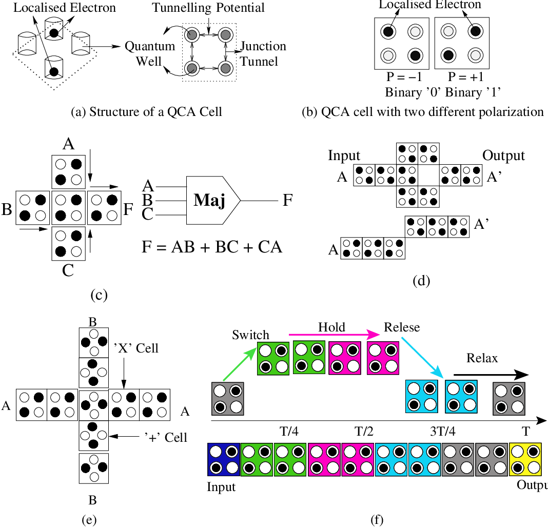
A QCA cell comprises of four quantum dots (Figure 1(a)) which can carry two free electrons. These free electrons can move between the four quantum dots. As shown in Figure 1(b), the two polarization states of a QCA cell can be represented as P=-1 (logic 0) and P=+1 (logic 1). The basic structures of QCA technology are majority voter (Figure 1(c)) and inverter (Figure 1(d)). The QCA majority voter (MV) can be expressed as,
MV(A, B, C) = AB + BC + CA
A majority voter can serve as a 2-input AND gate if one of the inputs is fixed at P=-1. Alternatively, if any one input of the majority voter is fixed at P=+1 then the modified majority voter can serve as a 2-input OR gate. There are two different types of inverter available in QCA technology as shown in Figure 1(d). The possible two orientations () and () ( and respectively) of QCA cell are shown in Figure 1(e). There are two fundamental wire-crossing techniques (co-planar and multi-layer) available in QCA. As shown in Figure 1(e), the co-planar wire-crossing can be implemented with the mix combination of two different orientations ( and ) of QCA cells. The multi-layer wire-crossing can be implemented with the help of two or more different layers. As discussed earlier, co-planar and multi-layer wire-crossing techniques are facing serious issues [14] [16] due to which we consider clock-zone based wire-crossing technique which can be implemented using non-adjacent clock zones (phase difference is equal to ) on the same plane [35][2] as shown in Figure 2. This eliminates the problem of interference between the QCA cells.

The QCA clock controls the flow of information within the circuit. The circuit information is carried from one end to another with the help of clock. The clock zones of QCA are distinct and phase shifted [42] [19]. At the time of computation, the previous clock zone must hold its output, which can be achieved by splitting the clock into four phases: switch, hold, release and relax [20] which is shown in Figure 1(f).
Four types of implementation technology exists in QCA: (a) metal-island [23]; (b) semiconductor [24]; (c) molecular [30] [9]; and (d) magnetic [37] [4]. The metal-island is the first implementation technology created to demonstrate the behaviour of QCA which requires cryogenic temperature to operate [23]. The semiconductor technology, now-a- days becomes operable in room temperature [17]. The semiconductor QCA technology is adopted as the implementation technology for our proposed QCA designs. The molecular technology, not yet implemented, is a single molecule implementation technology. This technology is highly promising due to its highly symmetric QCA cell structure, very high switching speeds, extremely high device density, operation at room temperature and even the possibility of mass-production by means of self-assembly. Magnetic QCA (MQCA) is based on the interaction between the nanoparticles of the magnet. The MQCA depends on the quantum mechanical nature of magnetic interactions, which can be operated at room temperature [37] [4].
3 Related Work

Limited attempts have been made to realize reconfigurable designs in QCA [27, 25, 28, 29, 31]. An And-OR-Inverter (AOI) logic is proposed in [25] where by fixing one or more input various logic functions can be implemented such as OR-AND, NAND-OR, NOR-NAND etc. which is shown in Figure 3(a). In [27], a complex 7-input QCA configurable gate (out of 7 inputs, 3 inputs are used as control inputs) is proposed by cascading three 3-input majority voter as shown in Figure 3(b). The sum of product, product of sum, four-input AND, four-input OR logic etc. can be constructed by fixing control inputs to “0” or “1”. In [31], under the presence of different QCA defects, a symmetric configurable fault tolerant reconfigurable gate (RFTG) has been proposed as shown in Figure 3(c). A novel configurable QCA design is proposed in [29]. The design (Figure 3(d)) is capable of realizing various logic functions such as 2-input OR, 3-input AND, 2-input OR, 3-input OR etc. A reconfigurable majority gate (Figure 3(e)) is presented in [28]. It is apparent that most of the previous work is limited to implement small logic functions only. Configurable memory structures in QCA are yet to be explored.
4 Proposed level triggered configurable flip-flop
The main advantage of realizing configurable hardware is low device cost and efficient utilization of device area. Till date, all the existing configurable designs in QCA strictly follow design rules mentioned below as in [29]:
- •
Fixing input cells (control inputs) to logic “0” or “1” to produce different functions.
- •
Displacing some of the input cells to change the distance between driver cells of the device to generate different functionality.
The first method is adopted to realize the proposed configurable designs as mentioned in [29]. To realize a configurable flip-flop, we first choose a JK flip-flop. The characteristic equation of JK flip-flop is . To produce D and T flip-flop, either a complemented value of input J or an un-complemented value of input J need to pass to both the inputs of JK flip-flop. The output function of XNOR is . If we choose B as a control input then we can use XNOR function as a simple QCA wire or an inverter. If B is zero then it will act as an inverter otherwise it will act as a simple QCA wire. So, the XNOR function can be used to produce a complemented value as well as an un-complemented value of its inputs controlling one of the inputs to zero or one. Moreover, a multiplexer is the best possible choice to select any one input between two input values.
The QCA representation of the proposed configurable flip-flop (CFF) is shown in Figure 4. The proposed CFF has 5 inputs (A, B, C1, C2 and CLK) and two outputs (Q and ) where C1, C2 are control inputs. The primary output of the proposed CFF is as follows:
| (1) | ||||
Case 1:
If C1 = C2 = 0 and CLK=1 then the equation 1 will be
Case 2:
If C1 = 0, C2 = 1 and CLK = 1 then the equation 1 will be
Case 3:
If C1 = 1, C2 = X (Don’t Care) and CLK = 1 then the equation 1 will be
The Table 1 shows the different functionality of the proposed CFF based on control inputs C1 and C2. The CFF will obey the rules of T FF if C1C2 = 01 and if C1C2 = 00 then CFF will behave as D FF. The CFF will behave as JK FF if C1C2 = 1X where X means don’t care. The truth table of the proposed CFF is shown in Table 2.
| Input (C1) | Input (C2) | Output (Q) |
| 0 | 0 | D FF |
| 0 | 1 | T FF |
| 1 | X | JK FF |
| X= Don’t Care | ||

| A | B | C1 | C2 | CLK | Q | Remark |
|---|---|---|---|---|---|---|
| 0 | 0 | 0 | 0 | 1 | 0 | D FF |
| 0 | 0 | 0 | 1 | 1 | 0 | T FF |
| 0 | 0 | 1 | 0 | 1 | 0 | JK FF |
| 0 | 0 | 1 | 1 | 1 | 0 | JK FF |
| 0 | 1 | 0 | 0 | 1 | 0 | D FF |
| 0 | 1 | 0 | 1 | 1 | 0 | T FF |
| 0 | 1 | 1 | 0 | 1 | 0 | JK FF |
| 0 | 1 | 1 | 1 | 1 | 0 | JK FF |
| 1 | 0 | 0 | 0 | 1 | 1 | D FF |
| 1 | 0 | 0 | 1 | 1 | 0 | T FF |
| 1 | 0 | 1 | 0 | 1 | 1 | JK FF |
| 1 | 0 | 1 | 1 | 1 | 1 | JK FF |
| 1 | 1 | 0 | 0 | 1 | 1 | D FF |
| 1 | 1 | 0 | 1 | 1 | 0 | T FF |
| 1 | 1 | 1 | 0 | 1 | 1 | JK FF |
| 1 | 1 | 1 | 1 | 1 | 0 | JK FF |
Module 1 (XNOR)
The function produced by this module is: . The output of module 1 is passed to module 2 as shown in Figure 4. Depending on the value of input C2, module 1 generates a complemented or un-complemented value of input A to module 2. If C2=0 then a complemented value of the input A is passed to module 2 otherwise uncomplemented value of input A is passed to module 2.
Module 2 (2:1 MUX)
The output function of this module is : . If C1=1, input B will be selected and module 3 will behave according to JK flip-flop. On the other hand, if C1=0, the module 3 will behave either D flip-flop or T flip-flop depending on the output F1. If then the module 3 will behave as a D flip-flop otherwise it will behave as a T flip-flop.
Module 3 (JK FF)
This module follows the instructions of module 1 and 2. Module 3 behaves as T flip-flop if module 1 produces F1 = A and at the same time module 2 produces F2 = F1 (Figure 5(a)). Alternatively, if module 1 produces and at the same time module 2 produces F2 = F1 then module 3 behaves as a D flip-flop. Finally, if module 2 produce F2 = B (module 1: F1= don’t care ) then module 3 behaves like a JK flip-flop.


| Design | Area | Cells | Clock | Layer | Configurable |
|---|---|---|---|---|---|
| Cycle | |||||
| The existing level triggered D FF | |||||
| In [22] | 0.20 | 104 | 1.25 | Single | No |
| In [40] | 0.08 | 66 | 1 | Single | No |
| In [18] | 0.05 | 48 | 1 | Single | No |
| In [32] | 0.04 | 36 | 1.50 | Single | No |
| The existing level triggered T FF | |||||
| In [22] | 0.20 | 108 | 1.25 | Single | No |
| In [40] | 0.10 | 90 | 1 | Single | No |
| In [10] | 0.08 | 69 | 1.25 | Single | No |
| In [36] | 0.06 | 68 | 1.25 | Single | No |
| In [5] | 0.06 | 46 | 1.50 | Single | No |
| The existing level triggered JK FF | |||||
| In [39] | 0.75 | 415 | 2.50 | Single | No |
| In [22] | 0.12 | 80 | 1.25 | Single | No |
| In [40] | 0.10 | 68 | 1 | Single | No |
| CFF | 0.20 | 159 | 2.75 | Single | Yes |
The advantage of configurable memory units lies in its application domain. These can be used to design circuits with architectural similarity eliminating the need to design separate hardware performing a specific function. For example, counters and shift registers can be implemented in a single design with the option to configure the flip-flop according to the need. The biggest advantage of the proposed CFF is that single module can serve as a D, T and JK FF. Table 3 shows the performance of CFF with the existing D, T and JK FF. The proposed CFF consists of delay covering an area of 0.20 with 159 QCA cells. Although, the proposed CFF exceeds in all the respect compared to existing designs, but these small overheads can be accepted due to the configurable superiority of CFF over the existing designs. All the previous designs [18] [22] [40] [32] [10] [36] [5] [39] are not configurable in nature and can produce only one function. On the other hand, the CFF can produce three different functions using the same circuit. Moreover, the CFF allows us to present an all in one flip-flop, which can also be perceived as a standard universal design. A universal, scalable, efficient (USE) realistic clock distribution scheme for QCA is proposed in [13]. The CFF layout under the USE clocking scheme (CFF-USE) is shown in Figure 6. The proposed CFF-USE consists of 541 QCA cells covering an area of 1.81 .




4.1 Memory design using proposed level triggered flip-flop
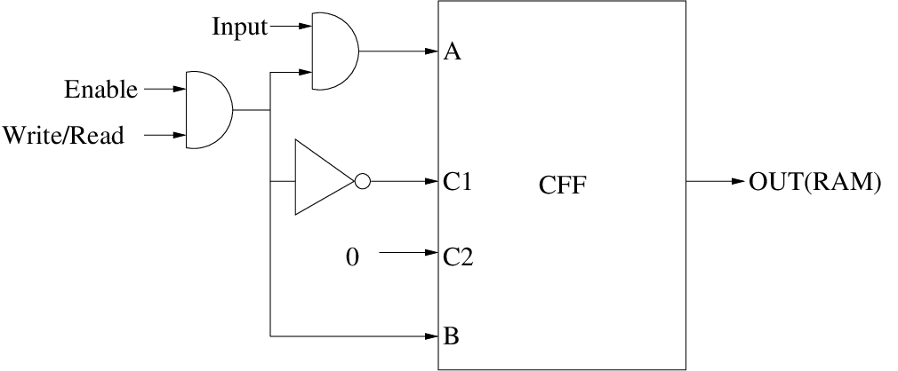
In this section, a 1-bit RAM is designed to test the proposed CFF functionality. All the pervious memory (RAM) designs in QCA can be categorized into two groups: line based and loop based. In the loop-based RAM design, four clock zones are utilized to store the previous value but in the line-based RAM design, a QCA wire is used to store the previous value of the output [7]. The proposed RAM design also utilizes the property of loop based design which is shown in Figure 7(b). The incoming input value is circulated inside the memory loop if the Enable input is set to 1 and at the same time Write/Read input is set to 0. If the Enable input is set to 1 and Write/Read input is 1 then the current stored value inside the memory loop is fed to the output. In both the cases i.e. read or write, the control input value of C2 is set to zero. The simulation result of the proposed RAM is shown in Figure 8. The inputs Enable and Write/Read are configured in such a way that they can provide the values needed for C1 and B input (Figure 7(a)). The proposed 1-bit RAM has 209 QCA cells covering an area of 0.31 .
5 Design of edge configurable flip-flop
The level triggered JK flip-flop is susceptible to noise due to which it leads to race-round condition [47]. In order to avoid such unstable phenomenon, edge triggered (falling, rising and dual) flip-flops are extensively studied. There are two well-known schemes in QCA to implement edge triggered flip-flop, the clock pulse generator scheme and the MUX/latch scheme [44]. In QCA, the clock pulse generator scheme is explored more than the MUX/latch scheme. Figure 9 shows the proposed pulse generator which can produce clock pulses for the falling edge, rising edge as well as dual edges with the help of the two control inputs C3 and C4. To detect a falling edge it takes the help of the previous clock pulse () and compares it with the current clock pulse (CLK). The is produced by using four consecutive clock zones (one clock cycle delay) as shown in Figure 9(b). The majority voter representation of the falling edge operation is as follows:


Out1= MV(MV(, C3, -1), , -1)
The value of (. ) will give a resultant boolean value of 1 which triggers a pulse in the output if the control inputs are set to C3=1 and C4=0 (Table 4). At the same time, the proposed clock pulse generator can generate rising edge (CLK ) which results to 1) if C3=0 and C4=1 (Table 4) and hence producing a trigger in the final output. The majority voter representation of the rising edge operation is as follows:
Out2= MV(MV(CLK, C4, -1), , -1)
The output of Out1 and Out2 (Figure 9(b)) is passed through an OR gate to produce the final output. If both the control inputs (C3=1 and C4=1) are set to 1 then the proposed clock pulse generator can produce pulses for both the edges (rising as well as falling) and hence works as a dual edge triggered clock pulse generator (Table 4). The majority voter representation of the dual edge operation is as follows:
Output=MV(Out1, Out2, 1)
| C3 | C4 | CLK | Out1 | Out2 | Output | |
| The falling edge operation of proposed clock pulse generator | ||||||
| 1 | 0 | 0 | 0 | 0 | 0 | 0 |
| 1 | 0 | 0 | 1 | 0 | 0 | 0 |
| 1 | 0 | 1 | 0 | 1 | 0 | 1 |
| 1 | 0 | 1 | 1 | 0 | 0 | 0 |
| The rising edge operation of proposed clock pulse generator | ||||||
| 0 | 1 | 0 | 0 | 0 | 0 | 0 |
| 0 | 1 | 0 | 1 | 0 | 1 | 1 |
| 0 | 1 | 1 | 0 | 0 | 0 | 0 |
| 0 | 1 | 1 | 1 | 0 | 0 | 0 |
| The dual edge operation of proposed clock pulse generator | ||||||
| 1 | 1 | 0 | 0 | 0 | 0 | 0 |
| 1 | 1 | 0 | 1 | 0 | 1 | 1 |
| 1 | 1 | 1 | 0 | 1 | 0 | 1 |
| 1 | 1 | 1 | 1 | 0 | 0 | 0 |
The job of the control inputs (C3 and C4) is to activate the pulse generator to get the necessary output pulse. The function of the control inputs are as follows:
- 1.
If C3=0 and C4=1 then the pulse generator acts as a rising edge triggered pulse generator.
- 2.
If C3=1 and C4=0 then the pulse generator acts as a falling edge triggered pulse generator.
- 3.
If C3=1 and C4=1 then the pulse generator acts as a dual edge pulse generator.
The simulation waveform of the proposed clock pulse generator is shown in Figure 10 which establishes the correctness of the proposed clock pulse generator.
The proposed edge configurable flip-flop (ECFF) (Figure 11) can be implemented with the help of a clock pulse generator (Figure 9) using CFF as the basic element. Efforts have been made to increase the functionality of ECFF by trying to incorporate a clock pulse generator whose effectiveness is determined by implementing all three types of pulses generated in a single design. The additional design is incorporated within the proposed structure to devise a configurable edge triggered flip-flop. The manifold advantage being that 9 different types of flip-flop designs usually done separately can be incorporated within one. This means the proposed ECFF can be reconfigured to falling edge D/T/JK FF, rising edge D/T/JK FF and dual edge D/T/JK FF using the same circuit. The simulation results of falling/rising/dual edge triggered JK FF is shown in Figure 12. The performance of the proposed ECFF is shown in Table 5. The existing dual edge triggered flip-flops are compared with the proposed ECFF which can be configured to falling edge D/T/JK FF, rising edge D/T/JK FF and dual edge D/T/JK FF using the same circuit. This means 9 different functions can be produced using the same ECFF whereas the existing flip-flops can produce only one function.


6 Realization of edge configurable n-bit counter/shift register
In this section, the edge configurable flip-flop is used as a basic element to realize the proposed counter/ shift register. In order to synchronize the clock of the proposed configurable counter/shift register one additional delay control circuit (DCC) (Figure 13) is introduced. The additional delay circuitry is used to delay the clock (fixing C3=0) by one complete cycle so that the clock can be synchronized. The function of the delay circuit is shown in Table 6.
| C3 | Delay | Current | Output |
| 0 | 0 | 0 | 0 |
| 0 | 0 | 1 | 0 |
| 0 | 1 | 0 | 1 |
| 0 | 1 | 1 | 1 |
| 1 | 0 | 0 | 0 |
| 1 | 0 | 1 | 1 |
| 1 | 1 | 0 | 0 |
| 1 | 1 | 1 | 1 |
The proposed configurable 2-bit counter/ shift register is shown in Figure 15. It can be configured to a shift register or a counter as necessary. The proposed configurable 2-bit counter/ shift register has 7 control inputs (C1, C1, C2, C2, C3, C4, C5), two primary inputs (A, B) and two primary outputs ( and ). The basic unit of the proposed counter/ shift register is the edge configurable flip-flop (CFF). A counter can be constructed using T or JK FF whereas shift register can be constructed using D FF. In the proposed 2-bit counter/ shift register, C1 and C2 inputs are used to adjust the CFF module to the required flip-flop whereas C5 input defines the behaviour of the circuit i.e. if C5=0 then the circuit behaves as a shift register otherwise it behaves as a counter. The two ECFF (configured as a D FF; C1=C1=0, C2=C2=0 and C5=0) are cascaded to design the proposed 2-bit shift register.

The 3-bit design of the proposed configurable counter/ shift register is shown in Figure 16. To synchronize the input and output of the 3-bit configurable counter/ shift register circuit, additional three delay control circuits need to be added to the ECFF module. The top delay control circuit is used to synchronize the output of the first module with rest modules whereas the bottom two delay control circuits are used to synchronize clock signal (CLK) of the proposed circuit. In the case of a 3-bit proposed edge configurable counter/ shift register, if C5=C6=0 then the circuit behaves as a shift register whereas if C5=C6=1 then the circuit will behave as a counter. Similarly, by cascading n-CFF modules, we can construct n-bit edge configurable counter/ shift register as shown in Figure 14 which can be configured to (dual/rising/falling) edge shift register as well as (dual/rising/falling) edge counter. The QCA representation of the proposed n-bit edge configurable counter/ shift register is shown in Figure 17. The performance of the proposed edge configurable counter/shift register is shown in Table 7. If we want to construct a shift register then there is no extra space requirement for the proposed configurable counter/ shift register due to its configurable nature hence it is more cost effective than the conventional designs. The main benefit of the configurable n-bit counter/shift register is that the same circuit can be configured to six different forms, (Dual/Falling/Rising) counter as well as (Dual/Falling/Rising) shift register.


| Design | Area | Cells | Clock | Single | Configurable |
|---|---|---|---|---|---|
| Cycle | Layer | ||||
| Existing 2-bit Counter | |||||
| In [43] | 0.74 | 430 | 4 | Yes | No |
| In [34] | 0.26 | 240 | 2 | No | No |
| In [6] | 0.22 | 141 | 2.25 | Yes | No |
| Proposed 2-bit Counter/shift register | 0.67 | 464 | 5.75 | Yes | Yes |
| Existing 3-bit Counter | |||||
| In [43] | 1.02 | 677 | 6 | Yes | No |
| In [34] | 0.48 | 428 | 2 | No | No |
| In [6] | 0.36 | 328 | 2.25 | Yes | No |
| In [3] | 0.22 | 196 | 2 | Yes | No |
| Proposed 3-bit Counter/shift register | 1.18 | 786 | 7.75 | Yes | Yes |

7 Simulation setup
QCADesigner (version 2.0.3) [41] has been used to verify the functional correctness of all the proposed QCA designs using both coherence vector and bistable approximation simulation engines using all the default parameters.
8 Conclusion
This paper attempts for the very first time, to design a level triggered configurable flip-flop (CFF) which can be used as a D, T and JK flip-flop as per the requirement. A 1-bit RAM is designed considering CFF as a basic element. Moreover, an edge configurable flip-flop (ECFF) is designed with the help of a clock pulse generator (CPG). The CPG can produce three different (rising/falling and dual) types of pulses using the same circuit. The edge configurable flip-flop (ECFF) can be used as 9 different flip-flops controlling only single module. An efficient edge configurable n-bit counter/shift register is proposed which can be configured as an n-bit counter or n-bit shift register as per the requirement.
Acknowledgement
This research is supported by the Department of Electronics and Information Technology, Ministry of Communications and IT, Government of India under the Visvesvaraya PhD Scheme administered by Media Lab Asia.
References
- (1) International technology roadmap for semiconductors (itrs) (2015)
- (2) Abedi, D., Jaberipur, G., Sangsefidi, M.: Coplanar full adder in quantum-dot cellular automata via clock-zone-based crossover. IEEE Transactions on Nanotechnology 14(3), 497–504 (2015)
- (3) Abutaleb, M.: Robust and efficient quantum-dot cellular automata synchronous counters. Microelectronics Journal 61, 6 – 14 (2017)
- (4) Alam, M.T., DeAngelis, J., Putney, M., Hu, X.S., Porod, W., Niemier, M., Bernstein, G.H.: Clocking scheme for nanomagnet qca. In: 2007 7th IEEE Conference on Nanotechnology (IEEE NANO), pp. 403–408 (2007). DOI 10.1109/NANO.2007.4601219
- (5) Angizi, S., Moaiyeri, M.H., Farrokhi, S., Navi, K., Bagherzadeh, N.: Designing quantum-dot cellular automata counters with energy consumption analysis. Microprocessors and Microsystems 39(7), 512 – 520 (2015). DOI http://dx.doi.org/10.1016/j.micpro.2015.07.011
- (6) Angizi, S., Moaiyeri, M.H., Farrokhi, S., Navi, K., Bagherzadeh, N.: Designing quantum-dot cellular automata counters with energy consumption analysis. Microprocessors and Microsystems 39(7), 512 – 520 (2015)
- (7) Angizi, S., Sarmadi, S., Sayedsalehi, S., Navi, K.: Design and evaluation of new majority gate-based {RAM} cell in quantum-dot cellular automata. Microelectronics Journal 46(1), 43 – 51 (2015)
- (8) Angizi, S., Sayedsalehi, S., Roohi, A., Bagherzadeh, N., Navi, K.: Design and verification of new n-bit quantum-dot synchronous counters using majority function-based jk flip-flops. Journal of Circuits, Systems and Computers 24(10), 1550,153 (2015). DOI 10.1142/S0218126615501534
- (9) Awais, M., Vacca, M., Graziano, M., Roch, M.R., Masera, G.: Quantum dot cellular automata check node implementation for ldpc decoders. IEEE Transactions on Nanotechnology 12(3), 368–377 (2013). DOI 10.1109/TNANO.2013.2251422
- (10) Bhavani, K.S., Alinvinisha, V.: Utilization of qca based t flip flop to design counters. In: Innovations in Information, Embedded and Communication Systems (ICIIECS), 2015 International Conference on, pp. 1–6 (2015). DOI 10.1109/ICIIECS.2015.7193059
- (11) Bobda, C.: Introduction to Reconfigurable Computing. Springer (2007)
- (12) Bondalapati, K., Prasanna, V.K.: Reconfigurable computing systems. Proceedings of the IEEE 90(7), 1201–1217 (2002). DOI 10.1109/JPROC.2002.801446
- (13) Campos, C.A.T., Marciano, A.L., Neto, O.P.V., Torres, F.S.: Use: A universal, scalable, and efficient clocking scheme for qca. IEEE Transactions on Computer-Aided Design of Integrated Circuits and Systems 35(3), 513–517 (2016). DOI 10.1109/TCAD.2015.2471996
- (14) Chaudhary, A., Chen, D.Z., Hu, X.S., Niemier, M.T., Ravichandran, R., Whitton, K.: Fabricatable interconnect and molecular qca circuits. Trans. Comp.-Aided Des. Integ. Cir. Sys. 26(11), 1978–1991 (2007). DOI 10.1109/TCAD.2007.906467
- (15) Chilakam, M.: A novel reconfiguration scheme in quantum-dot cellular automata for energy efficient nanocomputing. Master’s thesis, University of Massachusetts Amhers (2013)
- (16) Devadoss, R., Paul, K., Balakrishnan, M.: Coplanar qca crossovers. Electronics Letters 45(24), 1234–1235 (2009). DOI 10.1049/el.2009.2819
- (17) DiLabio, G., Wolkow, R., Pitters, J., Piva, P.: Atomistic quantum dot (2014). URL http://www.google.co.in/patents/US8816479. US Patent 8,816,479
- (18) Hashemi, S., Navi, K.: New robust {QCA} d flip flop and memory structures. Microelectronics Journal 43(12), 929 – 940 (2012). DOI http://dx.doi.org/10.1016/j.mejo.2012.10.007
- (19) Karkaj, E.T., Heikalabad, S.R.: A testable parity conservative gate in quantum-dot cellular automata. Superlattices and Microstructures 101, 625 – 632 (2017). DOI https://doi.org/10.1016/j.spmi.2016.08.054
- (20) Lent, C.S., Liu, M., Lu, Y.: Bennett clocking of quantum-dot cellular automata and the limits to binary logic scaling. Nanotechnology 17(16), 4240 (2006)
- (21) Lent, C.S., Tougaw, P.D., Porod, W., Bernstein, G.H.: Quantum cellular automata. Nanotechnology 4(1), 49 (1993)
- (22) Lim, L.A., Ghazali, A., Yan, S.C.T., Fat, C.C.: Sequential circuit design using quantum-dot cellular automata (qca). In: Circuits and Systems (ICCAS), 2012 IEEE International Conference on, pp. 162–167 (2012)
- (23) Liu, M., Lent, C.S.: High-speed metallic quantum-dot cellular automata. In: Nanotechnology, 2003. IEEE-NANO 2003. 2003 Third IEEE Conference on, vol. 2, pp. 465–468 vol. 2 (2003). DOI 10.1109/NANO.2003.1230946
- (24) Mitic, M., Cassidy, M.C., Petersson, K.D., Starrett, R.P., Gauja, E., Brenner, R., Clark, R.G., Dzurak, A.S., Yang, C., Jamieson, D.N.: Demonstration of a silicon-based quantum cellular automata cell. Applied Physics Letters 89(1), 013503 (2006). DOI http://dx.doi.org/10.1063/1.2219128
- (25) Momenzadeh, M., Huang, J., Tahoori, M.B., Lombardi, F.: Characterization, test, and logic synthesis of and-or-inverter (aoi) gate design for qca implementation. IEEE Transactions on Computer-Aided Design of Integrated Circuits and Systems 24(12), 1881–1893 (2005)
- (26) Momenzadeh, M., Ottavi, M., Lombardi, F.: Modeling qca defects at molecular-level in combinational circuits. In: 20th IEEE International Symposium on Defect and Fault Tolerance in VLSI Systems (DFT’05), pp. 208–216 (2005)
- (27) Motameni, H., Montazeri, B.: Reconfigurable logic based on quantum-dot cellular automata. Journal of Applied Sciences Research 7, 1817–1823 (2011)
- (28) Navi, K., Mohammadi, H., Angizi, S.: A novel quantum-dot cellular automata reconfigurable majority gate with 5 and 7 inputs support. Journal of Computational and Theoretical Nanoscience 12(3), 399–406 (2015)
- (29) Navi, K., Roohi, A., Sayedsalehi, S.: Designing reconfigurable quantum-dot cellular automata logic circuits. Journal of Computational and Theoretical Nanoscience 10(5), 1137–1146 (2013)
- (30) Pulimeno, A., Graziano, M., Sanginario, A., Cauda, V., Demarchi, D., Piccinini, G.: Bis-ferrocene molecular qca wire: Ab initio simulations of fabrication driven fault tolerance. IEEE Transactions on Nanotechnology 12(4), 498–507 (2013). DOI 10.1109/TNANO.2013.2261824
- (31) Roohi, A., Sayedsalehi, S., Khademolhosseini, H., Navi, K.: Design and evaluation of a reconfigurable fault tolerant quantum-dot cellular automata gate. Journal of Computational and Theoretical Nanoscience 10(2), 380–388 (2013)
- (32) Sabbaghi-Nadooshan, R., Kianpour, M.: A novel qca implementation of mux-based universal shift register. Journal of Computational Electronics 13(1), 198–210 (2014). DOI 10.1007/s10825-013-0500-9
- (33) Shamsabadi, A.S., Ghahfarokhi, B.S., Zamanifar, K., Movahedinia, N.: Applying inherent capabilities of quantum-dot cellular automata to design: D flip-flop case study. Journal of Systems Architecture 55(3), 180 – 187 (2009). DOI http://dx.doi.org/10.1016/j.sysarc.2008.11.001. Challenges in self-adaptive computing (Selected papers from the Aether-Morpheus 2007 workshop)
- (34) Sheikhfaal, S., Navi, K., Angizi, S., Navin, A.H.: Designing high speed sequential circuits by quantum-dot cellular automata: Memory cell and counter study. Quantum Matter 4(2), 190–197 (2015)
- (35) Shin, S.H., Jeon, J.C., Yoo, K.Y.: Wire-crossing technique on quantum-dot cellular automata. 2nd International Conference on Next Generation Computer and Information Technology 27, 52– 57 (2013)
- (36) Torabi, M.: A new architecture for t flip flop using quantum-dot cellular automata. In: Quality Electronic Design (ASQED), 2011 3rd Asia Symposium on, pp. 296–300 (2011). DOI 10.1109/ASQED.2011.6111764
- (37) Vacca, M., Graziano, M., Zamboni, M.: Majority voter full characterization for nanomagnet logic circuits. IEEE Transactions on Nanotechnology 11(5), 940–947 (2012). DOI 10.1109/TNANO.2012.2207965
- (38) Vankamamidi, V., Ottavi, M., Lombardi, F.: A serial memory by quantum-dot cellular automata (qca). IEEE Transactions on Computers 57(5), 606–618 (2008). DOI 10.1109/TC.2007.70831
- (39) Venkataramani, P., Srivastava, S., Bhanja, S.: Sequential circuit design in quantum-dot cellular automata. In: 2008 8th IEEE Conference on Nanotechnology, pp. 534–537 (2008). DOI 10.1109/NANO.2008.159
- (40) Vetteth, A., Walus, K., Dimitrov, V., Jullien, G.: Quantum-dot cellular automata of flip-flops. In: ATIPS Laboratory 2500 University Drive, NW, Calgary, Alberta, Canada T2N 1N4 (2003)
- (41) Walus, K., Dysart, T.J., Jullien, G.A., Budiman, R.A.: Qcadesigner: a rapid design and simulation tool for quantum-dot cellular automata. IEEE Transactions on Nanotechnology 3(1), 26–31 (2004). DOI 10.1109/TNANO.2003.820815
- (42) Wang, Y., Lieberman, M.: Thermodynamic behavior of molecular-scale quantum-dot cellular automata (qca) wires and logic devices. IEEE Transactions on Nanotechnology 3(3), 368–376 (2004)
- (43) Wu, C.B., Xie, G.J., Xiang, Y.L., Lv, H.J.: Design and simulation of dual-edge triggered sequential circuits in quantum-dot cellular automata. Journal of Computational and Theoretical Nanoscience 11(7), 1620–1626 (2014). DOI doi:10.1166/jctn.2014.3541
- (44) rong Xiao, L., xiong Chen, X., yan Ying, S.: Design of dual-edge triggered flip-flops based on quantum-dot cellular automata. Journal of Zhejiang University SCIENCE C 13(5), 385–392 (2012). DOI 10.1631/jzus.C1100287
- (45) Xiao, L.R., Xu, X., Ying, S.Y.: Dual-edge triggered t flip-flop structure using quantum-dot cellular automata. In: Nanotechnology and Precision Engineering, Advanced Materials Research, vol. 662, pp. 562–567. Trans Tech Publications (2013). DOI 10.4028/www.scientific.net/AMR.662.562
- (46) Yang, X., Cai, L., Zhao, X.: Low power dual-edge triggered flip-flop structure in quantum dot cellular automata. Electronics Letters 46(12), 825–826 (2010). DOI 10.1049/el.2010.1090
- (47) Yang, X., Cai, L., Zhao, X., Zhang, N.: Design and simulation of sequential circuits in quantum-dot cellular automata: Falling edge-triggered flip-flop and counter study. Microelectronics Journal 41(1), 56 – 63 (2010). DOI http://dx.doi.org/10.1016/j.mejo.2009.12.008