On the origin of Blue Luminescence in Mg doped GaN
Abstract
We uncover the origin of blue luminescence (BL) peak in Mg doped GaN thin film using a combination of experimental X-ray absorption near edge spectroscopy (XANES), first-principles calculations based on density functional theory and full multiple scattering theoretical analysis of various possible defect complexes and their XANES signatures. We demonstrate that a defect complex composed of Mg substituted at Ga site (MgGa) and Mg at interstitial site (Mgi) is primarily responsible for the observed BL by Donor-Acceptor Pair transition (DAP) associated with a deep donor state in the gap. It correlates with a higher (lower) oxidation state of N (Ga) in heavily Mg doped GaN than in its pristine structure, evident in our experiments as well as calculations. Physical and chemical mechanisms identified here point out a route to achieving efficient p-type GaN.
Keywords:
GaN:Mg, XANES, Defect complex, FEFF, SIESTAI Introduction
Gallium Nitride (GaN) is a wide band gap semiconductor (Eg = 3.51 eV at 2K) used for a wide variety of applications such as solid state lighting[1], high power and high frequency devices[2], and lasers[3]. It is essential to have both n and p-type semiconducting GaN to develop GaN/InGaN quantum well (QW) based optoelectronic devices. Despite intensive research in the last few decades, some material issues related to GaN remain open to be resolved. One of them is the unintentional n-doped behavior of native GaN; it is not clear whether it arises from point defects or from incorporation of impurities[4]. Although GaN based LEDs have already been commercialized, their optimal performance is yet to be realized, partly because of the difficulties in efficient incorporation of p-type carriers in the host. Till date, magnesium (Mg) is the only p-type dopant to have been successfully employed in fabrication of p-GaN. However, a high activation energy (or “ionization energy”) of Mg in GaN [5] ( 200 meV) requires relatively high concentration of Mg in fabrication of efficient p-GaN. Secondly, higher Mg incorporation in GaN leads to the formation of point defects and/or defect complexes, and consequent self-compensation in Mg doped GaN[6].
Incorporation of Mg in GaN results in characteristic luminescence peaks in Photo-luminescence (PL) and Cathodo-luminescence (CL) spectra depending on the dopant concentration. A small amount of Mg doping ( ) in GaN results in luminescence peaks at 3.270 and 3.466 eV (at T=2K)[7]. At higher Mg dopant concentration ( ) in GaN thin films, a dominant PL peak appears in the range of 2.70 - 2.95 eV, emitting blue luminescence (BL), the origin of which has been debated in the literature in the past decade[8, 9, 10, 11, 12, 13, 14]. Recent DFT-based calculations suggest that the emergence of BL is due to different ionization energies of nitrogen vacancies (VN) [15] and of hole localization at neighboring N atoms [16]. This however fails to explain the absence of BL from the samples with lower Mg-concentration. Moreover, no direct experimental evidence has been reported yet corroborating these mechanisms.
X-ray absorption near edge spectroscopy (XANES) is an effective probe to determine the element or site specific properties such as oxidation state of an atom, local geometry and the electronic structure[17]. Here, we report growth of undoped and Mg doped GaN thin films and their characterization with PL and XANES spectroscopies. We analyze the experimentally acquired XANES spectra by co-rrelating them with results of first-principles simulations of various defect complexes and decipher the characteristic features. Further, we use electronic structure of the relevant defect complexes obtained from DFT-based simulations to identify the luminescence centres in Mg doped GaN.
II Methods
II.1 Experimental Details
The films of GaN in Nanowall Network (NwN) geometry studied here were grown over (0001) plane of Sapphire by plasma assisted molecular beam epitaxy (PAMBE, SVTA-USA) system. The temperature of Gallium (Ga) effusion cell is maintained at 1030 oC. A constant nitrogen flow rate of 8 sccm (standard cubic centimeter per minute), substrate temperature of 630 oC, plasma forward power of 375 W and growth duration of 4 hours were used in growth of all the films. Mg and Ga fluxes are obtained from the beam equivalent pressure (BEP) and are varied by controlling K-cells temperature. Other growth related details can be found elsewhere[18]. We present analysis of three samples of GaN films here: one pristine (A) and two doped (namely B and C), where the sample C is grown with higher Mg flux (Mg:Ga=0.1102) than that used for B (Mg:Ga=0.0393). Optical properties of these films are studied with PL spectroscopy at an excitation wavelength of 325 nm. XANES spectra of these samples are recorded in total electronic yield (TEY) mode at SXAS beam line (BL-01) of the Indus-2 Synchrotron Source at Raja Ramanna Centre for Advanced Technology (RRCAT), Indore, India, in an ultrahigh vacuum (UHV) chamber with a base pressure of Torr. Optical system of the beamline contains toroidal mirror to focus the beam on sample surface (vertically as well as horizontally). The slit width before monochromator and sample are 1mm and 0.1 mm, respectively. The energy resolution in the acquired spectra is better than 0.2 eV. The details of the experimental setup for XANES measurements are given in reference 19. A typical data reduction procedure (background removal and normalization) of the XANES spectra is performed using the Athena software package [20].
II.2 Simulation Details
In the simulation of XANES spectra, we have carried out first-principles DFT calculations using a combination of many codes. First, we used the SIESTA code[21] to obtain the optimized atomic structure of defect configurations, where a Local Density Approximation (LDA) of Ceperley and Alder[22] with Perdew and Zunger [23] parametrization of the exchange and correlation energy functional was used. Integrations over Brillouin Zone of -GaN were sampled on a - centered uniform mesh of k-points in a unit cell of reciprocal space[24]. We relax positions of all atoms to minimize energy using a conjugate-gradients algorithm until the forces on each atom is less than 0.04 eV/Å. Our optimized lattice parameters of the pristine GaN are ‘a’ = 3.173 Å and ‘c’ = 5.163 Å, which are in good agreement with the experiment[25] (‘a ’= 3.186 Å and ‘c’ = 5.189 Å). In simulation of GaN with defect(s), we considered a supercell (128 atoms). From the relaxed atomic structure obtained from SIESTA calculations we constructed clusters in calculations to determine the ab-initio XANES spectra with FEFF9.05 code[26], where the Hedin-Lundqvist exchange potential with an imaginary part of 0.2 eV is used and an exchange core hole is treated according to the final state rule in simulation of K-edges. We calculated atomic potential for a 128 atoms cluster with a radius of 8 Å and determined the full multiple scattering XANES spectra by increasing the radius to 12.5 Å around the absorber. To determine electronic structure and gap states of the relevant defect configurations we used HSE06[27] hybrid functional as implemented in VASP code [28]. In these calculations, we used optimized lattice parameters and relaxed atomic structure obtained from SIESTA calculations (details of the numerical parameters used in VASP calculations are given in the section I of the Supplementary Information).
III Experimental Results
Details of the structural properties of the films studied here were discussed thoroughly in our earlier publication[18]. As mentioned earlier, we have chosen GaN NwN as the host in the present work because of the superior optical properties of the film. It is well known that[18, 29] GaN in NwN geometry do not show any other luminescence peak(s) except near band edge (NBE) ( at 3.4 eV) making it the preferred choice here. In the photoluminescence spectra obtained at RT (see Fig. 1), it is seen that the sample A has only one dominant luminescence peak centered at 3.43 eV, assigned NBE emission of GaN, whereas the sample B exhibit two distinct peaks, centered at 3.39 and 3.22 eV, respectively. While the peak centered at 3.39 eV is assigned to NBE of GaN, the peak centered at 3.22 eV is assigned to electron-Acceptor (e-A) or donor acceptor pair (DAP) transition in Mg-doped GaN[7]. PL spectra of sample C shows two distinct luminescence features, and they are identified as the NBE at 3.38 eV and the intense BL peak centered at 2.70 eV respectively.

To understand the origin of different luminescence peak as observed in the PL spectra of samples, it is useful to study the electronic structure of all samples. To this end, we have probed the N K-edge and Ga L2,3-edge of the three samples using XANES (see Fig. 2(a) and (d)). For N K-edge, five distinct features (P1-P5) are seen clearly, which are consistent with earlier observations[30]. We have considered the absorption edge as the location of the first significant peak in the first derivative of absorbance () with respect to energy (i.e. )[31] (see Fig. 2(b)). For each peak observed in Fig. 2(a) the corresponding maxima (P1’ -P5’) and minima (P1”-P5”) are shown in Fig. 2(b). It is seen that the N K-edges (P1’) of A and B do not show any significant changes in their absorption threshold, whereas that of sample C shows a shift of 0.7eV towards higher energy relative to that of A, suggesting a small increase in the oxidation state of N atoms in sample C. Along with a change in the absorption edge, we also observe a clear distortion of the peak P1. The peak intensity of P1 of sample C is higher and more pronounced than that of samples A and B (see inset of Fig. 2(c)). This increase in the peak intensity of P1 with higher Mg incorporation is consistent with an earlier report[32]. Increase in the intensity of the feature P1 may arise from the localized states that form due to higher Mg incorporation in the film. We further observe a small absorption feature at 400.16 eV (see arrow in Fig. 2(a) and Fig. 2(c)).

Recorded L2,3 edge spectra of Ga atoms are presented in Fig. 2(d), with the first derivative of L3 edge in the inset. Similar to N K-edge, we do not observe any changes in the absorption threshold of samples A and B. However, we observe a small red shift ( 0.80 eV) in that of sample C, indicating reduction in the oxidation states of Ga atoms in sample C. The two distinct features R1 and R2 are seen clearly in all three samples. For samples A and B, the intensity of R1 is higher than that of R2, whereas for the sample C, intensity of R2 is higher than that of R1, with a flat absorption profile near the L3 edge.
IV Theoretical Analysis and Discussion
IV.1 X-ray Absorption Near Edge Structure
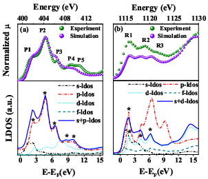
To uncover the origin of observed changes and features in experimental XANES spectra as a function of Mg doping concentration, we have obtained ab-initio XANES spectra. We focus on three possible mechanisms, which are widely speculated to be the origins of the BL in literature: (i) nitrogen vacancy complexes, (ii) the configuration with hole localization and (iii) Mg interstitial defect complex (ball and stick model of the different defect configurations are shown in Fig.S1 of section III of the Supplementary Information). Before studying the relevance of vacancy complexes to XANES spectra, we benchmarked the simulation parameters with careful analysis of the pristine GaN. Fig.3 (a) and (b) show theoretical XANES spectra of N K-edge and Ga L3 edge respectively, along with the experimentally observed spectra from a flat GaN epitaxial layer. Clearly, there is a good agreement between our theory and experiment (see Fig. 3), as well as the results reported earlier[33].
We observe that N K-edge absorption edge is primarily dominated by the unoccupied N-2p orbitals, whereas Ga L3 edge has a strong ‘s+d’ hybridized orbital character. Further, we find that the feature R1 has a strong ‘s+d’ hybridized character, and R2 and R3 are predominantly ‘d’ character. The calculated local density of states (LDOS) projected on s, p, and d orbitals of N and Ga atoms reveal narrow energy sub-bands (marked with “” ) in agreement with the energies of the characteristic features seen in the XANES spectra.
The simulated N K and Ga L3 edges in XANES spectra of the substitutional Mg at Ga site (MgGa) are shown in Fig. 4(a) and (b) respectively. We find that peak P1 obtained from the simulation of configuration with (MgGa) defect is not very prominent, and has a lower intensity relative to the pristine GaN. This reduction in intensity of P1 is consistent with the behavior shown by sample B, and we infer that no other defect complexes are present notably in sample B and the luminescence peak centered at 3.22 eV is due to recombination of electron-Acceptor pair (e-A). Mulliken population analysis from results of SIESTA calculations suggests a small increase in the oxidation states of both 1st nearest neighbor (NN) N ( 0.05 ) atoms as well as 1st NN Ga ( 0.016) atoms, that co-ordinate the site of Mg substituent in Mg-doped GaN relative to that of undoped GaN (see Table 1). Despite this small increase in oxidation states of N and Ga atoms seen in our simulations, we do not observe a significant change in absorption edges of the sample B, due to significantly lower incorporation of Mg in the host.
Further, we simulated several defect configurations such as (i) complexes of MgGa with a single N vacancy (Mg), with two N vacancies (Mg), with Mg at interstitial site (Mg) (ii) complex of Mg at interstitial site with a nitrogen vacancy (Mg), (iii) Mg at Nitrogen site (antisites) (MgN), and (iv) Mg at interstitial site (Mgi). The characteristic signatures of these configurations in the XANES spectra are shown in Fig. 4(a) and (b). In the configurations of Mg, we have considered N-vacancies in the axial and basal planes of the -GaN, as the four Ga-N bond lengths are not same for GaN4 tetrahedra. We find that former configuration is energetically more preferable, and do not observe any significant change in the characteristics of XANES spectra with respect to pristine GaN. Thus, the increase in the peak P1 of sample C cannot be attributed to formation of a Mg complex.

A comparison between the experimental and simulated results for XANES spectra clearly suggests that the possible causes for the enhanced intensity of P1feature in N K-edge of the sample C can be Mg, Mg, Mg or . Mulliken charges of N atoms, near these defect complexes due to formation of defect complexes are listed in Table 1 along with the formation energies. Clearly the oxidation states of N (Ga) atoms increase (decrease) slightly in these defect configurations. Thus, a clear conclusion on determination of dominant defect(s) could not be reached from the Mulliken population analysis alone. Further, our estimates of the formation energies of these defect complexes obtained using Zhang-Northrup scheme [34] (see Table 1 and details on the method used for calculation of defect formation energy in section II of Supplementary Information) reveal that the defect configuration Mg has the lowest formation energy, and is probably the most preferable defect complex that should form in Mg-doped GaN. Recently, Miceli et al.[35] and Reshchikov et al.[36] predicted from Hybrid functional based DFT calculations that Mg interstitial is the energetically preferable defect in Mg-doped GaN, which was neglected earlier due to over-estimation of its formation energy with a semilocal functional[37, 38], which is consistently evident in the results of our calculations here (see Tab.1). Simulated L3 edge spectra of the configurations Mg and show (see Fig. 4(b)) that the peak R2 has a higher intensity than R1, as observed experimentally only for the sample C.
Thus, we propose that the observed increase in intensity of P1 of sample C is due to the increase in the unoccupied donor states, originating from the formation of defect complex Mg and/or . Further the shift in the absorption threshold of N-K edges of sample C in comparison to sample A is due to reduction in the Mulliken charges (oxidation states) of N atoms of the MgN4 tetrahedra. We find the relaxed atomic structure of GaN containing the Mg defect complex shows elongation of axial Mg-N bond by 14%, while in basal plane one Mg-N bond in the basal plane contracts by 2.5% while other two Mg-N bond stretches by 5.4% relative to the Ga-N bonds of pristine GaN.
To connect with the prediction of Van de Walle et al.,[16] we simulate the XANES spectra of N K and Ga L3 edges by stretching the Mg-N bond to a value 15% higher than the Ga-N bond, while allowing other atoms to relax (see Fig. 4). We do not see any significant change in the N K-edge w.r.t. pristine GaN. Thus, the distortion of peak P1 in Fig.2 (a) can not be attributed to longer Mg-N bond. A careful observation of the simulated N K-edge spectra in Fig. 4(a) reveals an absorption edge (at 400 eV) for all the N-vacancy related complexes thus we attribute this feature at 400.16 eV in the XANES spectra (see Fig.2(c)) to unoccupied states associated with N-vacancies.
| Defect complex | Formation Energy | Mulliken charge in | |
|---|---|---|---|
| (in eV) | NN N | NN Ga | |
| 1.20 | -0.050 | -0.016 | |
| 0.51 | -0.015 | +0.152 | |
| 4.91 | -0.046 | +0.181 | |
| 8.47 | -0.056 | +0.242 | |
| 9.78 | -0.064 | +0.074 | |
| -0.17 | -0.061 | +0.055 | |
| 4.80 | -0.015 | +0.068 | |
IV.2 Electronic Energy Levels
As DFT-LDA typically underestimates the band gap (band gap of GaN calculated with SIESTA is 2.06 eV, much lower than its experimental value of 3.51 eV (see section IV of the Supplementary Information)), we used hybrid HSE06 functional based calculations to determine energy levels of the defect states in the electronic structure using VASP code (see Fig.7). In these simulations with a supercell, we used only -point in sampling the Brillouin Zone integrations. Our estimate of the band gap of pristine GaN is 3.36 eV, reasonably close to the experimentally observed band gap of 3.51 eV at T=2K and 3.43 eV observed at RT in this study. For the configuration MgGa, we find a shallow acceptor state ( 0.22 eV above the VBM), which has a predominant N-2p orbital character. Configurations with (Mg) and Mgi exhibit deep donor states in the electronic gap at 3.14 and 3.07 eV above VBM. Thus, the transitions from the deep donor states to the shallow acceptor state occur at ( eV), very close to the emission peak of BL (here 2.7 eV) observed in sample C (see Fig.7). We note that the concentration of Mg in our simulations of Mg-doped GaN is higher than experiment, and this small difference is partly due to that.

Although in past, a similar mechanism (transition between deep donor to shallow acceptor) on the origin of BL has been proposed, its atomistic origin has not been clear[39, 10] . Lyons et al.[16] claimed an alternative mechanism where BL is a result of transitions of electrons from the conduction band to the deep and localized MgGa acceptor level. However, it fails to explain large shifts in the BL peak with increase in excitation intensity and absence of thse same in lightly doped samples. In addition, work of Buckeridge et al. [15] suggests that the BL may be due to the formation of isolated N-vacancy where authors used a hybrid quantum mechanical (QM) and molecular mechanical (MM) embedded cluster method. In contradiction to this, reports claimed that isolated N vacancy gives rise to yellow luminescence (2.18 eV) [40] and/or green luminescence (2.35 eV) in Mg doped GaN [36]. Also, some issues related to the accuracy in calculations of Buckeridge et al.[15] have been reported by other groups[41, 42]. Recently, Wahl et al.[43] studied the site occupancy of Mg in GaN by implanting radioactive Mg in GaN, and found a notable amount of Mg in interstitial sites, while the majority of them occupy the substitutional Ga sites. As mentioned earlier, some reports [35, 36] suggest the formation energy of Mg occupying at interstitial site is less in p-type GaN. Thus, Mg may prefer to be at the interstitial sites in the films during the epitaxial growth process.
As the epitaxial growth temperature of GaN is reasonably high (630 oC in the present work), mobility of Mg adatom is high during growth. When Mg at interstitial site diffuses close to a Ga vacancy site in the process, it takes up the same and becomes substitutional Mg at Ga site in GaN[43]. In the films grown under the low Mg flux, occurrence of MgGa is expected to be dominant, resulting in formation of a shallow acceptor state in the electronic gap, and associated 3.22 eV peak in the luminescence spectra. In contrast, during the epitaxial growth with higher Mg flux, the number of available Ga vacancy sites are not abundant enough for diffusing Mgi to get converted to MgGa. Instead, Mgi adatoms will pair up with other suitable defects due to their relatively low formation energy and form defect complexes such as Mg, which create a deep donor state in the electronic gap. Our work shows that these are responsible for the BL emission arising from the deep donor to shallow acceptor state transitions. Further, the mechanism proposed in this study on the origin of BL clearly explain the the large shift of peak position with increase in excitation intensity and absence of BL in lightly doped samples. Based on our analysis, we propose that the synthesis of p-type GaN under lower Ga flux (Ga poor condition) will be an efficient way relative to higher flux.
V Summary
We have uncovered the origin of observed BL in Mg doped GaN through a combination of experiments and theoretical analysis of Mg incorporated at different concentration GaN thin films. With clear evidence in PL and XANES of heavily Mg incorporated GaN films, we show that the observed BL originates from defect complexes formed of interstitial Mg (Mgi) and substitutional Mg (MgGa). The BL is associated with a transition from the deep donor state in electronic gap to shallow acceptor state. Our experiments reveal a slightly higher oxidation state of N and lower oxidation state of Ga in heavily Mg incorporated GaN than those in pristine GaN, which are supported well by our first-principles calculations.
Acknowledgments
The authors thank Professor C. N. R. Rao for his support and guidance. SN acknowledges DST for a Senior Research Fellowship. The authors gratefully acknowledge JNCASR, UGC-DAE CSR and RRCAT, Indore for providing facilities. UVW acknowledges support from a JC Bose National Fellowship and a TUE-CMS project funded by Nano Mission, Department of Science and Technology, Government of India.
References
- [1] R. D. Dupuis, M. R. Krames, and S. Member, J. Light. Technol. 26, 1154 (2008).
- [2] S. T. Sheppard, K. Doverspike, W. L. Pribble, S. T. Allen, J. W. Palmour, L. T. Kehias, and T. J. Jenkins, IEEE Electron Device Lett. 20, 161 (1999).
- [3] T. C. Lu, T. T. Kao, S. W. Chen, C. C. Kao, H. C. Kuo, and S. C. Wang, Appl. Phys. Lett. 92, 141102 (2008).
- [4] C. G. Van De Walle and J. Neugebauer, J. Appl. Phys. 95, 3851 (2004).
- [5] M. Zhang, P. Bhattacharya, W. Guo, and A. Banerjee, Appl. Phys. Lett. 96, 132103 (2010).
- [6] I. P. Smorchkova, E. Haus, B. Heying, P. Kozodoy, P. Fini, J. P. Ibbetson, S. Keller, S. P. DenBaars, J. S. Speck, and U. K. Mishra, Appl. Phys. Lett. 76, 718 (2000).
- [7] B. Monemar, P. P. Paskov, G. Pozina, C. Hemmingsson, J. P. Bergman, S. Khromov, V. N. Izyumskaya, V. Avrutin, X. Li, H. Morkoc, H. Amano, M. Iwaya, and I. Akasaki, J. Appl. Phys. 115, 053507 (2014).
- [8] R. Nonoda, K. Shojiki, T. Tanikawa, S. Kuboya, R. Katayama, and T. Matsuoka, Jpn. J. Appl. Phys. 55, 05FE01 (2016).
- [9] L. Eckey, U. von Gfug, J. Holst, A. Hoffmann, A. Kaschner, H. Siegle, C. Thomsen, B. Schineller, K. Heime, M. Heuken, O. Schön, and R. Beccard, J. Appl. Phys. 84, 5828 (1998).
- [10] M. Reshchikov, G.-C. Yi, and B. Wessels, Phys. Rev. B 59, 13176 (1999).
- [11] E. Oh, H. Park, and Y. Park, Appl. Phys. Lett. 72, 70 (1998).
- [12] U. Kaufmann, P. Schlotter, H. Obloh, K. Köhler, and M. Maier, Phys. Rev. B 62, 10867 (2000).
- [13] S. Hautakangas, V. Ranki, I. Makkonen, M. J. Puska, K. Saarinen, L. Liszkay, D. Seghier, H. P. Gislason, J. A. Freitas, R. L. Henry, X. Xu, and D. C. Look, Phys. B Condens. Matter 376-377, 424 (2006).
- [14] S. Hautakangas, K. Saarinen, L. Liszkay, J. Freitas, and R. Henry, Phys. Rev. B 72, 165303 (2005).
- [15] J. Buckeridge, C. R. A. Catlow, D. O. Scanlon, T. Keal, P. Sherwood, M. Miskufova, A. Walsh, S. M. Woodley, and A. A. Sokol, Phys. Rev. Lett. 114, 016405 (2015).
- [16] J. L. Lyons, A. Janotti, and C. G. Van De Walle, Phys. Rev. Lett. 108, 156403 (2012).
- [17] H. Wende, Reports Prog. Phys. 67, 2105 (2004).
- [18] S. K. Nayak, M. Gupta, and S. Shivaprasad, RSC Advances 7, 25998 (2017a).
- [19] D. Phase, M. Gupta, S. Potdar, L. Behera, R. Sah, A. Gupta, C. Murli, D. Bhattacharyya, and S. Gadkari, in AIP Conference Proceedings, Vol. 1591 (AIP, 2014) pp. 685–686.
- [20] B. Ravel and M. Newville, Journal of Synchrotron Radiation 12, 537 (2005).
- [21] J. M. Soler, E. Artacho, J. D. Gale, A. Garcia, J. Junquera, P. Ordejon, and D. Sanchez-Portal, J. Phys. Condens. Matter 14, 2745 (2001).
- [22] D. M. Ceperley and B. J. Alder, Phys. Rev. Lett. 45, 566 (1980).
- [23] J. P. Perdew and A. Zunger, Phys. Rev. B 23, 5048 (1981).
- [24] H. J. Monkhorst and J. D. Pack, Phys. Rev. B 13, 5188 (1976).
- [25] M. Leszczynski, I. Grzegory, H. Teisseyre, T. Suski, M. Bockowski, J. Jun, J. Baranowski, S. Porowski, and J. Domagala, J. Cryst. Growth 169, 235 (1996).
- [26] J. J. Rehr, J. J. Kas, F. D. Vila, M. P. Prange, and K. Jorissen, Phys. Chem. Chem. Phys. 12, 5503 (2010).
- [27] J. Heyd, G. E. Scuseria, and M. Ernzerhof, The Journal of Chemical Physics 118, 8207 (2003).
- [28] G. Kresse and J. Furthmüller, Phys. Rev. B 54, 11169 (1996).
- [29] S. K. Nayak, D. Shamoon, J. Ghatak, and S. M. Shivaprasad, Phys. Status Solidi A 214, 1600300 (2017b), 1600300.
- [30] W. R. L. Lambrecht, S. N. Rashkeev, B. Segall, K. LawniczakJablonska, T. Suski, E. M. Gullikson, J. H. Underwood, R. C. C. Perera, J. C. Rife, I. Grzegory, S. Porowski, and D. K. Wickenden, Phys. Rev. B 55, 2612 (1997).
- [31] E. M. Bittar, C. Adriano, T. M. Garitezi, P. F. S. Rosa, L. Mendonça-Ferreira, F. Garcia, G. D. M. Azevedo, P. G. Pagliuso, and E. Granado, Phys. Rev. Lett. 107, 267402 (2011), arXiv:1107.0962 .
- [32] Y. C. Pan, S. F. Wang, W. H. Lee, W. C. Lin, C. I. Chiang, H. Chang, H. H. Hsieh, J. M. Chen, D. S. Lin, M. C. Lee, W. K. Chen, and W. H. Chen, Solid State Commun. 117, 577 (2001).
- [33] M. S. Moreno, K. Jorissen, and J. J. Rehr, Micron 38, 1 (2007).
- [34] S. B. Zhang and J. E. Northrup, Phys. Rev. Lett. 67, 2339 (1991).
- [35] G. Miceli and A. Pasquarello, Physical Review B 93, 165207 (2016).
- [36] M. A. Reshchikov, D. Demchenko, J. McNamara, S. Fernández-Garrido, and R. Calarco, Physical Review B 90, 035207 (2014).
- [37] C. G. Van de Walle, J. Neugebauer, C. Stampfl, M. McCluskey, and N. Johnson, ACTA PHYSICA POLONICA SERIES A 96, 613 (1999).
- [38] J. Neugebauer and C. G. V. de Walle (Proceedings of the Materials Research Symposia of Gallium Nitride and Related Materials, edited by R. D. Dupuis, J. A. Edmond, F. A. Ponce, and S. Nakamura (Materials Research Society, Pittsburgh, Pennsylvania,1995)) p. 645.
- [39] H. Teisseyre, T. Suski, P. Perlin, I. Grzegory, M. Leszczynski, M. Bockowski, S. Porowski, J. A. Freitas, R. L. Henry, A. E. Wickenden, and D. D. Koleske, Phys. Rev. B 62, 10151 (2000).
- [40] Q. Yan, A. Janotti, M. Scheffler, and C. G. Van de Walle, Applied Physics Letters 100, 142110 (2012).
- [41] D. O. Demchenko and M. A. Reshchikov, Phys. Rev. Lett. 115, 029701 (2015).
- [42] J. L. Lyons, A. Alkauskas, A. Janotti, and C. G. Van de Walle, physica status solidi (b) 252, 900 (2015).
- [43] U. Wahl, L. M. Amorim, V. Augustyns, A. Costa, E. David-Bosne, T. A. L. Lima, G. Lippertz, J. G. Correia, M. R. da Silva, M. J. Kappers, K. Temst, A. Vantomme, and L. M. C. Pereira, Phys. Rev. Lett. 118, 095501 (2017).
Additional information
V.1 Numerical parameters used in VASP calculation
First-principles DFT calculations were carried out using a plane-wave projector augmented wave (PAW) method as implemented in the VASP code, where a Local Density Approximation (LDA) of Ceperley and Alder is used for the exchange and correlation energy functional. The reference valence elecronic configurations of Ga, N and Mg were considered as , and , respectively. We used an energy cutoff of 500 eV to truncate plane wave basis. Electronic energy spectrum at point was calculated by using Heyd-Scuseria- Ernzerhof (HSE) hybrid functional, where the mixing parameter for the Hartree-Fock exchange potential is set at 25%. The screening parameter in HSE calculations is fixed at 0.2.
V.2 Procedure to calculate defect formation energy
Formation energy of defects (for neutral state) in the bulk was calculated using Zhang-Northrup scheme, given by
where and are the total energies of super-cells containing a defect and the reference pristine structure, respectively. and represent the number of atom added or removed (if atom(s) are added it will take positive sign where as if atom(s) are removed it will take -ve sign) and chemical potential of species, respectively. In this work, we have calculated the defect formation energy under N rich conditions. Under N rich conditions is the energy of N- atom (obtained from the total energy of molecule, i.e. ). The chemical potential of Ga is calculated using the assumption of thermodynamic equilibrium, ; where is the total energy of one formula unit of bulk w-GaN. We have used chemical potential of Mg () as the energy of single Mg atom in the hcp phase (, noting that the primitive unit cell of hcp structure contains two atoms.
V.3 Atomic Models Used for DFT and FMS calculation

V.4 Electronic structure of defect complexes
