High Surface Conductivity of Fermi Arc Electrons in Weyl semimetals
Abstract
Weyl semimetals (WSMs), a new type of topological condensed matter, are currently attracting great interest due to their unusual electronic states and intriguing transport properties such as chiral anomaly induced negative magnetoresistance, a semi–quantized anomalous Hall effect and the debated chiral magnetic effect. These systems are close cousins of topological insulators (TIs) which are known for their disorder tolerant surface states. Similarly, WSMs exhibit unique topologically protected Fermi arcs surface states. Here we analyze electron–phonon scattering, a primary source of resistivity in metals at finite temperatures, as a function of the shape of the Fermi arc where we find that the impact on surface transport is significantly dependent on the arc curvature and disappears in the limit of a straight arc. Next, we discuss the effect of strong surface disorder on the resistivity by numerically simulating a tight binding model with the presence of quenched surface vacancies using the Coherent Potential Approximation (CPA) and Kubo–Greenwood formalism. We find that the limit of a straight arc geometry is remarkably disorder tolerant, producing surface conductivity that is a factor of 50 larger of a comparable set up with surface states of TI. Finally, a simulation of the effects of surface vacancies on TaAs is presented, illustrating the disorder tolerance of the topological surface states in a recently discovered WSM material.
I I. Introduction
While Weyl semimetals have long been studied for their condensed matter realization of relativistic massless (Weyl) fermions[1], and related particle physics phenomenon such as the chiral anomaly[2], only recently have they attracted great interest[3, 4, 5, 6, 7, 8, 9] for extending concepts of Topological Insulators [10, 11, 12] (TI) to gapless systems.


Topological Insulators (TIs) are time–reverse symmetric states of matter characterized by an insulating bulk which exhibits unique highly conductive metallic surface states. In the case of 3D TIs, the surface states consist of a massless 2D Dirac fermion dispersion relation with characteristic helical spin–momentum locking and a circular Fermi surface (Figure 1a). This spin–momentum locking results in the suppression of backscattering (k to –k) from non–magnetic impurities since states with opposite spin and momentum remain orthogonal as along as time–reverse symmetry is respected. As a result, the surface transport of 3D TIs is uniquely robust to non–magnetic disorder.
In contrast, Weyl semimetals can only occur if either time–reversal or inversion symmetry is broken and are characterized by a bulk band structure which is fully gapped except at isolated points where the electronic structure is represented by the 2x2 Weyl Hamiltonian. Each Weyl point acts as a positive or negative monopole of Berry flux depending on whether its chirality is +1 or -1. Since the total Berry flux through the WSM Brillouin Zone must be zero, Weyl points always appear in pairs of opposite chirality[13]. The surface electronic states of WSMs are subsequently described by arc states (Figure 1b) which are topologically protected as long as the bulk 3D Weyl points remain intact[3].
The topological protection in WSMs means that the Weyl points cannot be gapped by infinitesimal perturbations and can only disappear by merging with a Weyl point of opposite chirality in which case they form a double degenerate Dirac point[14] that is generally susceptible to small perturbations. Depending on the path the Weyl points take in reciprocal space, the arc states can either collapse to a point, or form a closed contour, where gapping the resulting Dirac points may result in either a trivial or topological insulator phase.
There are always two arcs that connect each set of Weyl points due to the existence of two (top and bottom) surfaces of the material. They can, for example, manifest themselves in quantum oscillatory techniques[15]. While there is no general spin–momentum locking mechanism for the Fermi arc states, backscattering of electrons from the arc associated with the top surface to the arc associated with the bottom surface is forbidden due to zero spatial overlap between the corresponding electronic states. Hence, considering transport perpendicular to the orientation of the arcs, the situation is similar to the case of TIs.
The unique electronic states in Weyl semimetals, along with their topological origin, makes it appealing to study their charge transport mechanism. This was the subject of intense study lately[5, 16, 17, 18, 19, 20, 21, 22] where Weyl points have been found to be robust against weak bulk disorder although it was argued that going beyond perturbative RG approaches may induce a small density of states even at weak disorder[23, 24]. With the bulk density of states disappearing as where is the energy of the Weyl points away from the nodal point and is the velocity of the Fermi electrons, the bulk DC conductivity in a clean free fermion limit is expected to be zero[3] at zero temperature and , although disorder, interactions, and thermal excitations modify this result. With a characteristic strength of the impurity potential , the scattering rate for the electrons in Born approximation and the conductivity remains finite even at [5]. Interactions alone were found to acquire a linear temperature dependence[16] and reproduce a clean fermion limit. A more complete study of bulk dc transport and ac optical properties of 3D Dirac and Weyl semimetals including their temperature dependence and doping away from the nodal point was recently elaborated in details[22].
The existence of the topologically protected surface states leads to another set of interesting phenomena. For example, the surface conductivity in 3D TIs was extensively investigated[27, 28, 29, 30, 31, 32], and its disorder tolerance has been emphasized. The Fermi arcs in WSMs gives rise to a non–zero anomalous Hall effect with a semiquantized value of the Hall conductivity proportional to the distance between the Weyl points[4, 5]. The impurity scattering via the Fermi arcs has been studied in dilute bulk disorder limit using Born approximation in a most recent work[25] where the dissipative nature of the surface currents in WSMs has been highlighted and the effect of surface–to–bulk scattering was emphasized.
In order to examine the conductivity of the Fermi arc electrons in Weyl semimetals, we need to introduce a notion of surface conductivity in general. In a standard setup, a homogeneous electric field is applied across the sample, and the conductivity relates the current density as a linear response to the applied field. We now wish to find the current density that appears as the response to the electric field existing in a part of space, such as a sample surface. A general linear response relationship is given by
where we restrict the field by a part of space. A standard Kubo–Greenwood approach applies for very general perturbations [26]. This results in the same technicalities in computing as for the bulk conductivity with the matrix elements of electron velocity operators now restricted by the area where . For an insulator, such as the 3D TI, this brings nothing new, since the current in the system with bulk energy gap can only be carried by the surface Fermi electrons, and there is no need to restrict the applied field by the sample surface. However, in a WSM, spatially homogeneous fields will always produce a non–zero bulk current due to thermal excitations, disorder and electronic correlations even in ideal scenarios with the Fermi level pinned at the Weyl points[5, 16]. In thermodynamic limit, such current will overwhelm all surface effects. Physically, however, we expect that the Fermi arc electronic states extending well into the bulk near the Weyl points, are capable of supporting strong surface currents, therefore understanding their scattering cross sections both within the surface and into the bulk is an important problem that we address in the present work.
An experimental setup that can probe surface conductivity can be easily sketched. We imagine a double–tip Scanned Tunneling Microscope (STM) design[61] as illustrated in Figure 2. Two STM tips are scanned across the surface of the WSM sufficiently close to each other so that the temperature dependent part of the mean path of the electrons at the surface is comparable with the distance between the tips but much larger than the average distance between surface impurities . This can always be achieved at sufficiently low temperatures. The applied voltage between the tips has to be sufficiently small, so that the corresponding electric field decaying quickly into the bulk will disturb only a thin layer close to the surface. As two tips traverse through the WSM surface, the local disorder affects the mean free path of the surface states, and the robustness of the Fermi arc electrons can be directly probed.

Here, we focus on the surface charge transport in WSMs and discuss two major relaxation mechanisms contributing to it. We first present a qualitative discussion of electron–phonon scattering where we find that its contribution strongly depends on the shape of the Fermi arc and becomes vanishingly small in the limit of a straight arc. This conclusion is virtually independent of the particular form of the electron–phonon matrix elements, but results from the fact that, in the limit of a straight arc, scattering only occurs between states with the same velocity along the direction of the current. Next, we perform numerical studies of the effect of strong surface disorder on the surface conductivity in WSMs. Using a tight–binding model in the slab geometry, we utilize a Coherent Potential Approximation (CPA)[33], a self–consistent theory that has been widely used for studies of substitutional alloys at arbitrary concentrations, to investigate the effect of quenched surface vacancies on the electronic spectral functions. We then calculate the slab conductivity using the Kubo–Greenwood formalism. Our model takes into account the scattering processes within the arc and from the arc to the bulk Weyl points. We find that the WSM model with a straight Fermi arc is remarkably disorder tolerant, producing a surface conductivity that is about 50 times larger than the comparable set–up with circular surface states of the 3D TI model. By computing the optical reflectivity, we also find that our WSM model with straight arc behaves as an ideal polarizer for incident light. Finally, a discussion is given for the applicability of our results to real WSMs discovered recently[6, 7]. We apply the CPA technique to study the effect of surface vacancies in TaAs where we find that the topological Fermi arc states display a robustness to disorder in a real material setting.
II II. Electron–Phonon Scattering
The electron–phonon contribution to the resistivity of metals has long been understood both qualitatively[36] and using first principle electronic structure calculations based on the density functional linear response approach[37]. In the linear temperature regime, the electron–phonon resistivity can be written as where effects due to the Fermi electrons and their interactions with phonons is contained in the transport electron–phonon coupling constant which is given by the following integral over the Brillouin Zone[36],
| (1) | |||||
Here, and are the energies and velocities of Fermi electrons, and is the matrix element of the potential induced by the displacement of atoms from their equilibrium positions associated with a phonon of wavevector (we omit summations over phonon branches for simplicity).
Although electron–phonon resistivity calculations can be carried out for real materials using first principles methods [37], to gain physical insight into how the Fermi arc geometry influences the resistivity, we first consider a minimal model for a single arc consisting of a segment of a circle of radius that carries a fixed density of states where is the length of the arc, is the angle the arc spans along the circle and is the velocity of the arc electrons which is assumed to be the same as the Fermi velocities of the bulk Weyl points. The limit of a straight arc is obtained by sending to infinity, to zero and keeping the length fixed, while the circular Fermi surface characteristic of 3D TIs is recovered when is equal to the Fermi wavevector , , and . We assume the arc to be symmetric with respect to y axis, and consider the applied electric field along y–axis. Note that although this model reproduces a smooth transition from the circular surface states of TI to the case of a straight Fermi arc, it should not be interpreted as modeling a literal transition between a WSM and TI since in an actual material, merging the Weyl points may collapse the arc.


We can consider the scattering phase space which contributes to the transport coefficient by taking the electron–phonon scattering matrix element to be a constant in the expression for However, to ensure that spin–momentum locking is recovered in the TI limit where , we assume that the spin is always tangential to the arc. For the isotropic Weyl model illustrated in Figure 1b this is approximately the case near the middle of the arc. With this spin arrangement, the spin dependent part of the matrix element is given by,
| (2) |
which reflects the overlap between spinor states at and . The dependence of the phase space integral can be evaluated numerically. Figure 3 shows the result for an arc with (Figure 3a) and a complete circle with (Figure 3b). A remarkable observation is that in the limit of a straight arc, the phase space collapses as contributions by 90 degree scattering processes are all suppressed since electrons are scattered between states with the same velocity along the direction of the current. This makes the factor in the expression for (where for the transport along the y–axis we take ). In the TI limit of the Fermi circle, one sees that 180 degree backscattering processes with wavevector are forbidden due to the orthogonality of spinor states with opposite spin orientations and that contributions by 90 degree scattering processes (described by in Fig 3b) are similarly suppressed since the velocity of the electrons projected onto the direction of the current remains the same after scattering.
To provide a more realistic wave vector dependence for the electron–phonon matrix elements we can consider a deformation potential type model with and additionally include a Debye model for screening in 2D
| (3) |
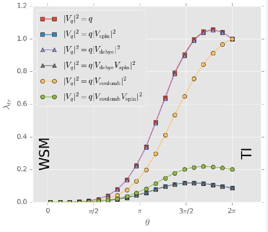
where the Debye screening constant is assumed to be (for simplicity we choose the case of a free relativistic electron gas in 2D[43] although one can also introduce the static dielectric constant of the substrate material such as the bulk TI). Figure 4 illustrates our calculated transport coupling constant as a function of the arc curvature described by the angle for several choices of the electron–phonon matrix elements which we represent it as a product of the spin and spatial parts: We distinguish the case with and the case given by equation (2) to account for the spin structure of the electronic states along the arc. We also distinguish cases with , and as the extreme limit of the 2D bare Coulomb repulsion. The transport coupling constant is normalized to unity in the limit of a complete circle () when using
A few observations can be made. First, the transport coupling constant is very small for arc geometries where and completely disappears in the limit of a straight arc. Second, the spatial dependence of the electron–phonon matrix elements as given by the constant, the Debye screening and the bare Coulomb models, only weakly influences this result. Third, the spin structure of the arc states leads to a reduction of the scattering by a factor of 2–8.
We now discuss the low temperature dependence of the surface resistivity. The 2D surface states of WSM should result in a behavior which becomes linear in once it raises above the characteristic Debye energy of phonons . This is primarily due to the observation that the energy of Fermi electrons in a metal is normally much larger than In the opposite limit, the crossover occurs at the so called Bloch–Grüneisen temperature, which was, for example, a well established case for graphene[34, 35] and could be realized for the WSMs with anomalously small Fermi arcs. We provide complete analysis of the temperature dependent electron–phonon scattering in Appendix A.
Our general conclusion is that the intra–arc contribution to the electron–phonon resistivity in WSMs may become vanishingly small in the limit that the arc approaches a straight line which makes this transport mechanism more effective than the circular Fermi surfaces of the TIs.
III III. Impurity Scattering
The contribution to the resistivity by electron–impurity scattering is another important mechanism of charge transport in metals, and the influence of bulk impurities on electronic scattering in Weyl systems has been extensively studied in a number of recent works [16, 17, 18, 19, 20, 21, 25]. Since Weyl points remain intact in the presence of weak bulk disorder, an important question arises on the influence of surface disorder, which is known to have a significant impact on the surface transport properties of such well–studied topological insulator system as Bi2Se3[38, 39].
In a real sample, surface disorder can be substantially strong, hence the Born approximation which is typically used in the analysis of impurity scattering may not be adequate. We therefore utilize the Coherent Potential Approximation (CPA)[33], a self–consistent theory of alloys that simulates random disorder up to arbitrarily strong concentrations. In particular, the method allows us to simulate quenched surface vacancies which is one of the primary forms of surface disorder in many materials. The method explicitly incorporates scattering events between states within the arc and from the arc to the bulk Weyl points which are slightly affected by the presence of strong surface disorder. Note however that when the vacancy concentration reaches 100% (a complete removal of a single surface layer), the electronic states should recover their values at zero concentration. One of the major limitations of the CPA approach is the lack of Anderson localization effects. Fortunately, this is not a serious issue when considering massless fermions in 2D[40] although a strong bulk disorder may lead to localization for 3D Dirac fermions[20, 21].
For the WSM, we consider a realistic tight–binding model with only two bulk Weyl points [41]. Using a slab geometry that is infinite in xy directions and finite in the z direction (c–axis) this model shows a single straight Fermi arc that is extended between the Weyl points located at . To compare the result of our simulation with the limit of a circular Fermi surface, we also consider a realistic tight–binding model of TI [42] which shows a surface Dirac cone located around the point. The parameters of both models are adjusted so that the Fermi velocities and densities of states remain the same in both simulations (See Appendix B for details). This setup allows us to directly compare the effect of the arc geometry on the conductivities which we determine using the Kubo–Greenwood formalism.

First, we discuss how the presence of surface disorder affects the spectral functions. Figure 5 shows the imaginary part of the self–energy describing the life time effects of the surface states that is obtained from our CPA simulation for both models as a function of vacancy concentration on the top and bottom layers. We find that for the WSM model is approximately two orders of magnitude smaller than the imaginary part of the self–energy for TI. This is partly due to the fact that the TI Dirac cone is mainly a pure surface state[32] while the arc states extend well into the bulk once they approach Weyl points and become insensitive to the surface disorder. Our result implies that the mean impurity scattering rate of the WSM surface is significantly smaller than in TI. The Fermi level for the TI should be placed at to match the density of states of the WSM. However, the imaginary part of the self–energy is essentially independent of the Fermi level in TI as long as we stay in the vicinity of the Dirac point (we show two results for and on Figure 5) as was discussed in a recent work[32].

To provide a direct comparison between the charge transport properties in the WSM and TI cases, we have used the Kubo–Greenwood formalism with the self–energies obtained from our CPA simulation to calculate the slab conductivities for both models. Figure 6 gives the zero temperature DC conductivity for the WSM as a function of surface vacancy concentration for an electric field perpendicular to the orientation of the arc as well as the conductivity for the TI. As a result of the smaller imaginary part of the self–energy, and the suppression of scattering contributions for the straight arc, the zero temperature DC conductivity of the WSM is much less affected by surface vacancies than that for TI. We find the difference between the two conductivities to be around 50. This result advances the idea of realizing a more disorder tolerant surface charge transport than that proposed for TIs as it appears that, in the limit of weak bulk disorder, the Fermi arc surface states of WSMs are more robust to the presence of surface vacancies than the surface states of TIs.

The unique geometry of the straight arc with its Fermi velocities in the perpendicular direction results in interesting consequences for the optical properties of our WSM model. For the bulk Weyl and Dirac cone states, this topic has been recently studied in detail both theoretically[22] as well as experimentally[44] for a Dirac semimetal ZrTe5. However, accounting for the arc–to–bulk optical transitions alters the response functions and results in strongly anisotropic optical properties.
Using the Kubo–Greenwood formalism, we have calculated the optical (AC) conductivity for our WSM slab setup with a surface disorder of for light polarized along the arc (x–axis) and in the perpendicular direction (y–axis). Figure 7 plots the calculated reflectivity, where we see that the reflectivity for y–polarized light exhibits a classical metallic behavior while the reflectivity for x–polarized light is semi–metallic, exactly as it was found in several recent works[22, 44]. Thus, a single straight arc acts as an ideal polarizer for reflected light (for frequencies above phonons), an interesting effect with possible applications in optics.
IV IV. Results for Real Materials: TaAs Weyl Semimetal
Physical insight gained from our simulations on models are now discussed in the context of real materials that have been discovered in the past few years to show WSM behavior. This broad class of solids includes systems such as TaAs[6, 7, 45], NbP[46], TaP[47], NbAs[48], as well as so called type–II WSMs such as MoTe2[49], MoP2, WP2[50], WTe2[51], and LaAlGe[52]. Despite sharing many common properties, such as a chiral anomaly induced negative magnetoresistance effect[53], their detailed topological properties are very different. LaAlGe has 40 Weyl nodes and TaAs has 24 nodes while TaIrTe4[54] shows only 4, the minimal number allowed in an inversion symmetry breaking system. In addition, some WSMs such as TaAs[45] and NbAs[48] show very short and curved Fermi arcs, while HgTe–class of WSM shows large circular Fermi arcs[55] and WSMs such as Ta3S2[56], TaIrTe4[54] and MoxW1-xTe2 [57] show very long and straight Fermi arcs. A large diversity here offers a unique platform to develop topological electronic devices[58], and the guiding principles how the arc geometry affects its transport properties can be very useful in real world scenarios.
Recently, several approaches have been proposed to engineer the shape and length of the Fermi arcs by introducing appropriate doping[57]. While bulk doping may lead to more significant contributions from arc–to–bulk scattering and the multiplicity of arcs would necessarily assume inter–arc scattering of the electrons, projecting the surface states onto certain crystallographic directions or manipulating the arcs spin structures by varying strength of spin–orbit coupling using substitutions[59] are possible ways to suppress those effects. All this makes control of topological surface transport a promising research direction.
To illustrate the robustness of the Fermi arcs to surface disorder in a real material setting, we consider TaAs as an example. We perform ab initio electronic structure of TaAs surface in a 6 unit–cell–long slab geometry using Density Functional Theory in its Generalized Gradient Approximation. We subsequently simulate the effect of quenched surface vacancies using self–consistent CPA theory which we run for a range of concentrations to explore the evolution of the electronic spectral functions (See Appendix C for complete details). TaAs is a complex system and exhibits a variety of states in the vicinity of the Fermi level including regular bulk Fermi states, doped Weyl points as well as ordinary surface states and the Fermi arcs. They all have been carefully mapped out by recent ARPES[6, 7] and quasiparticle interference [60] experiments.
Figure 8 shows evolution of the Fermi states of the TaAs slab structure that are projected onto the As terminated surface for various concentrations of substitutional vacancies that we impose at topmost As layer of the slab, ranging from =0.05 to =0.3, Figs.8(a–d). For smaller concentrations of vacancies, x=0.05–0.1, 8(a,b), we note well defined (horseshoe–like) Fermi arcs connecting bulk Weyl points that we call type 1. They have been widely discussed in recent TaAs literature [7, 60]. Also, there are other states (stretching along and lines) which are composed from the bulk Fermi electrons that are projected onto the surface Brillouin Zone, as well as bow–tie looking surface states seen at the endings of those structures (in the vicinity of and points). There should exist another set of Fermi arcs around and points which originate from the Weyl points called type 2. Unfortunately, there is some discrepancy in the current literature related to the position of these arcs. Sometimes they were associated with straight lines connecting the points 1 and 2, or with very short lines connecting the only points 2 or with the bow–tie shaped structure around points and [6, 7, 60]. Nevertheless, it is clear that, as the disorder increases, the surface states get broadened by the self–energy effects which is seen for both regular surface states as well as for the arc states. However, since the arc electrons are continuously connected to the bulk Weyl points, the areas in the vicinity of the Weyl points remains largely unaffected by disorder. This is in contrast to the regular surface states which are expected to be more susceptible to disorder. As there is no bulk disorder in our simulation, the bulk states are largely unaffected by the surface vacancies.

V V. Conclusion
In conclusion, we have analyzed the effects of electron–phonon scattering and quenched surface vacancies on the surface charge transport properties via the Fermi arcs. Our simulations on models showed that in the limit of a straight arc and disorder free bulk, the contributions of both scattering mechanisms to the resistivity are significantly suppressed and the Fermi arcs can support a near dissipationless surface current. This allows us to bring interesting parallels between 3D topological insulators and ideal Weyl semimetals: The former are non conductors in the bulk and exhibit metallic conductivities at the surface, while the latter show a bad metallic conductivity at the bulk but high charge conductivity at the surface.
At the end, we also demonstrated that the Fermi arcs remain disorder tolerant in TaAs. Although it is challenging to discuss the part of conductivity connected to the Fermi arcs due to multiplicity of other effects, such as thermal excitations, finite bulk disorder as well as contributions from regular Fermi electrons, we suggest that either thin films samples or experimental double–tip STM design can be useful for studying surface charge transport mechanism in real Weyl semimetals.
VI Acknowledgement
The authors acknowledge useful conversations with Xi Dai, G. Kotliar, E. da Silva Neto, W. Pickett, R. Singh, A. Vishwanath, H.M Weng, D. Yu. This work was supported by the US National Science Foundation Grant DMR–1411336 (S.Y.S.).
VII Appendix A. Semicircular Arc Model

Here we consider contributions to electron–phonon coupling arising from scattering within a minimal model for a single Fermi arc illustrated in Figure 9. The model consists of a segment of a circle of radius which subtends an angle and ends at a pair of the Weyl points. For our calculations, the length of the arc is assumed to be constant. Hence, the angle is related to the curvature of the arc. The particle is assumed to have the relativistic dispersion relation along the arc. Hence, the velocity of the particle has a constant magnitude and is orientated perpendicular to the arc. For the Weyl point, we assume they are located at the ends of the arc with each having the dispersion
Consider electric field along the axis which is the axis of symmetry for the arc. Recall that within the Boltzman theory, the electron–phonon resistivity
is expressed via the so called transport spectral function as follows (we use atomic units with
where are the phonon frequencies, are the absolute squares of the electron–phonon matrix elements and
are the mean squares of the Fermi velocities. In the following assume the Debye approximation with for with the maximum wavevector determined by the Debye frequency and the sound velocity Also assume that the matrix element of the electron–phonon scattering depends only on the transferred momentum
as this is the case for the deformation potential type model where
or including the Debye screening
where or for 2D/3D cases respectively. With these approximations we obtain
where the transport phase space is the integral over the Brillouin Zone
We can include spin dependence of the matrix elements assuming, for example, that the spins are tangential to the arc. By representing
we assume that
Although this may not be the case for the straight arc with isotropic bulk Weyl points of opposite chirality, such alignment will result in a correct limit when the arc turns into the full circle with the spin momentum locking characteristic of a 3D TI.
Consider now three cases of intra–arc scattering, scattering within the Weyl points and arc–to-bulk scattering.
VII.1 Intra–arc scattering.
All integrals are taken in 2D. The area unit cell is given by We first obtain
For the transport phase space integral we obtain in polar coordinates where is the angle with respect to
where the maximum scattering angle is given by
The expression is valid for For the transport spectral function we obtain
where the expression in square brackets assumes possible forms of the electron phonon matrix elements.
The resistivity behavior can be analyzed for the two regimes and set by the Bloch Grüneisen temperature (
For the regime we obtain the resistivity linear in
with the transport constant
Note that and disappears in the limit of the straight arc.
For the regime the resistivity behavior is determined by the low frequency expansion of We obtain the resistivity
The generalization for the angles is straightforward. In particular, we give the answers for the case of the circle with the radius We obtain
Here the Bloch–Grüneisen temperature is set by
In the limit we obtain the resistivity linear in
Note here that the inclusion of the spin dependence set by in the matrix element reduces the coupling constant by 2–5 times depending on a particular form of the spatial matrix element.
For the regime the resistivity behavior is determined by the low frequency expansion of We again obtain the resistivity
VII.2 Weyl Point Scattering
All quantities are now referred to the unit cell of the 3D solid. For the bulk scattering within a single Weyl point set by the isotropic dispersion in 3D we obtain
Here the Fermi wave vector assumes a doping away from the nodal point. The transport phase space integral in spherical coordinates with measured away from z axis we obtain
For the transport spectral function assume for simplicity the deformation potential electron–phonon matrix element The result is given by
The Bloch–Grüneisen temperature is set by
In the limit we obtain for the bulk resistivity per volume
It shows the behavior linear in
Note that if the (in the vicinity of the nodal point) we obtain independent behavior
In the limit , the is very small for and we can set the upper limit of integration to The resistivity shows behavior
where the value of the integral here is 0.202. Note the resistivity grows as approaches the nodal point.
VII.3 Arc–To–Bulk Scattering.
Here we have to either assume that we measure the conductivity within a finite slab of the width or we define the current within a thin surface layer by applying electric field only within this layer, since in the bulk thermodynamic limit ( the bulk conductivity will scale proportional to and overwhelm all surface effects. The transport spectral function
includes transitions within the Weyl points projected onto the slab Brillouin Zone, within the arc, and the arc–to–WP transitions, . Note that the normalization factor here is proportional to the slab size
where we approximate the contribution from the Weyl point by its bulk value per unit cell times the number of unit cells in the slab given by We note that includes the transitions between various projections of the same bulk state now appeared in the surface Brillouin Zone, but they are orthogonal to each other. This will collapse the double sum to a single sum over which is proportional to . At the absence of the surface scattering, such scaling in the numerator will be cancelled with appeared in the denominator and will not depend on The resistivity has additional prefactor of therefore will scale as which simply gives the result that the conductivity of the slab is the conductivity per unit cell volume times the number of unit cells in the slab. For the finite the transitions within the Weyl point will disappear when and so will the arc–to–WP transitions. Therefore the resistivity will be determined by the intra–arc scattering alone. This result will hold as long as is finite.
VIII Appendix B. Lattice Models for Weyl Semimetal and Topological Insulator
We consider the following minimal two–band 3D Weyl semimetal model on a simple cubic lattice [41],
| (4) |
The model breaks time reverse symmetry and contains two Weyl nodes of opposite chirality at . For all of our calculations we again set the lattice constants to unity, and use the parameters , , , and . To simulate the Fermi arc surface states we use a cubic lattice which is infinite along axis but which has layers along the z–axis. The Fermi arc is the straight line which connects the two Weyl nodes at in momentum space.
In the vicinity of a Weyl point the Hamiltonian can be written in a general form[62]
| (5) |
where is either positive or negative unity, is the velocity of the particle along the respective axis, and the chirality of the Weyl node is the product Usually, isotropic case is discussed, where the electron spin along the arc must change its orientation (at least once) while traversing between the Weyl nodes of opposite chirality ( see Figure 10a). However, our minimal model assumes a more general anisotropic case where spin retains the same orientation along the entire length of the arc (see Figure 10b).
The following minimal four–band model is used to simulate a 3D Topological insulator on a simple cubic lattice with nearest–neighbor hopping [42],
| (6) |
where the Dirac matrices are given in terms of the Pauli matrix via the relations,
For all of our simulations we set the lattice constants to unity, and use the parameters . To simulate surface states, we use a cubic lattice which is infinite along the –axis but which has sites along the z–axis with two spins per each site. The band structure contains a doubly degenerate 2D Dirac cone centered at the point consisting of states that are exponentially localized on opposing surfaces of the slab structure. The bulk band structure is fully gapped.
These parameters were chosen to insure that the velocity of the TI Dirac cone and the velocity of the WSM Fermi arc are approximately equivalent. In the case of TI, the Fermi level matches the density of states of WSM at We explored two levels close to the Dirac point ( and ) while in the case of WSM the Fermi level was taken to be pinned to the Weyl nodes ().


For the simulations with disorder a complex energy–dependent self–energy is obtained by using a Coherent Potential Approximation which is then utilized in calculating the conductivities using Kubo–Greenwood formalism. For integrals over the Brillouin Zone, that appear in Kubo–Greenwood calculation, we use two complementary methods, a simple k–point summation and a tetrahedron method. For simple k–sums, we found that we need to use enormous numbers of grid points, up to 4000x4000, to reach complete convergency of the calculated conductivities. We also developed a new tetrahedron method for integrating products of two Green functions exhibiting two poles in a complex plane. The method has been previously used in its simplified version[63, 64] to calculate transport and optical properties for strongly correlated systems, and is now generalized for arbitrary cases of energy band degeneracies at the corners of the tetrahedron. We found that the tetrahedron method allows us to use much coarser grids, 120x120, in order to reproduce the results obtained from the fully convergent k–sum integration.
IX Appendix C. Simulation of surface vacancies for TaAs using Coherent Potential Approximation
We determine the one–electron energy states of 6 unit–cell (24 atomic layers) slab structure using density functional theory (DFT) with generalized gradient approximation (GGA) for the exchange–correlation potential[65] as implemented in the full potential linear muffin–tin orbital (FP–LMTO) method[66]. In order to perform simulation of vacancies on the topmost As layer, we implement a coherent potential approximation, a self–consistent dynamical mean field approach that allows to extract disorder induced self–energies from the FP–LMTO calculation
The Coherent Potential Approximation is a self–consistent method that allows to determine by reducing the problem to a single scatterer problem embedded into the effective medium. It relies on separating the single particle Hamiltonian onto the hopping term and on–site scattering term . For two pure systems A and B this implies the forms
With a given initial guess for self–energy the local Green function of the disordered medium is computed
It defines the so called bath Green’s function
containing hybridization effects of the local scatterer with the medium. The scatterers A and B embedded into the medium are now described by the ”impurity” Green functions
from which the effective scatterer of the disordered medium is simply viewed as the weighted average
This equation defines new self–energy at the iteration that is then used to compute new and the entire procedure is repeated until self–consistency over (or equivalently over ) is reached.
Our implementation of these CPA equations is based on their combination with Density Functional Theory using a projector operator technique similar to as strongly correlated materials are studied using a combination of DFT and dynamical mean field theory (DMFT) methods[67]. To set up the DFT+CPA method, we define a site dependent projector operator
with help of radial solutions of the one–electron Schroedinger equation taken with a spherically symmetric part of the full potential. The disorder induced dynamical self–energy at site is now defined with help of the projectors
and used to construct local Green’s function of the lattice
where the matrix elements of the are taken using the LMTO basis set
We now define scattering potentials and in reference to pure systems. For the problem at hand, we treat the original slab structure of TaAs as a pure system A, and the same slab structure with top As layer removed as a pure system B. This can be achieved by adding a very large potential to each surface As atom that effectively un–hybridizes the top As layer from the rest of the slab. The vacancy induced self–energy is viewed as the correction to the Hamiltonian of pure system A, hence we set and (technically, a very large number, 10,000). The self–consistent CPA procedure is then utilized after which the surface Greens functions (slab Green functions projected onto 4 topmost atomic layers) are visualized on Fig. 8 of the main text.
References
- [1] For a review, see, e.g., G. E. Volovik, The Universe in a Helium Droplet, (Clarendon, Oxford, England, 2003).
- [2] H. B. Nielsen and M. Ninomiya, Phys. Lett. 130 B, 389 (1983).
- [3] X. Wan, A. M. Turner, A. Vishwanath, and S. Y. Savrasov, Phys. Rev. B 83, 205101 (2011).
- [4] Kai-Yu Yang, Yuan-Ming Lu, and Ying Ran, Physical Review B 84, 075129 (2011).
- [5] A. A. Burkov, L. Balents, Phys. Rev. Lett. 107, 127205 (2011).
- [6] B. Q. Lv, H. M. Weng, B. B. Fu, X.P. Wang, H. Miao, J. Ma, P. Richard, X. C. Huang, L. X. Zhao, G. F. Chen, Z. Fang, X. Dai, T. Qian, and H. Ding, Phys. Rev. X 5, 031013 (2015).
- [7] Su-Yang Xu, Ilya Belopolski, Nasser Alidoust, Madhab Neupane, Guang Bian, Chenglong Zhang, Raman Sankar, Guoqing Chang, Zhujun Yuan, Chi-Cheng Lee, Shin-Ming Huang, Hao Zheng, Jie Ma, Daniel S Sanchez, BaoKai Wang, Arun Bansil, Fangcheng Chou, Pavel P Shibayev, Hsin Lin, Shuang Jia, M Zahid Hasan, Science 349, 613 (2015).
- [8] For a review, see, e.g., Pavan Hosur, Xiaoliang Qi, Comptes Rendus Physique, 14, 857 (2013).
- [9] For a review, see, e.g., N.P. Armitage, E. J. Mele, Ashvin Vishwanath (unpublished).
- [10] For a review, see, e.g., M. Z. Hasan and C. L. Kane, Rev. Mod. Phys. 82, 3045 (2010).
- [11] For a review, see, e.g., J. E. Moore, Nature 464, 194 (2010).
- [12] For a review, see, e.g., Xiao-Liang Qi and Shou-Cheng Zhang, Physics Today 63, 33 (2010).
- [13] Nielsen, H.B.; Ninomiya, M. Phys. Lett. B 105: 219 (1981).
- [14] S. A. Parameswaran, T. Grover, D. A. Abanin, D. A. Pesin, and A. Vishwanath, Phys. Rev. X 4, 031035 (2014).
- [15] Andrew C. Potter, Itamar Kimchi & Ashvin Vishwanath, Nature Comm. 5, 6161 (2014).
- [16] Pavan Hosur, S. A. Parameswaran, and Ashvin Vishwanath, Charge Transport inWeyl Semimetals, Phys. Rev. Lett. 108, 046602 (2012).
- [17] Zhoushen Huang, Tanmoy Das, Alexander V. Balatsky, and Daniel P. Arovas, Phys. Rev. B 87, 155123 (2013).
- [18] Rudro R. Biswas, and Shinsei Ryu, Physical Review B 89, 014205 (2014).
- [19] Björn Sbierski, Gregor Pohl, Emil J. Bergholtz, and Piet W. Brouwer, Phys. Rev. Lett. 113, 026602 (2014).
- [20] J. H. Pixley, Pallab Goswami, and S. Das Sarma, Phys. Rev. Lett. 115, 076601 (2015).
- [21] S. V. Syzranov, L. Radzihovsky, and V. Gurarie, Phys. Rev. Lett. 114, 166601 (2015).
- [22] C. J. Tabert, J. P. Carbotte, and E. J. Nicol, Phys. Rev. B 93, 085426 (2016).
- [23] Nandkishore, R., D. A. Huse, and S. L. Sondhi, Phys. Rev. B 89, 245110 (2014).
- [24] Pixley, J. H., D. A. Huse, and S. Das Sarma, Phys. Rev. X 6, 021042 (2016).
- [25] E. V. Gorbar, V. A. Miransky, I. A. Shovkovy and P. O. Sukhachov, Phys. Rev. B 93, 235127 (2016).
- [26] See, e.g., G. D. Mahan, Many–Particle Physics Plenum, New York (1990).
- [27] Dimitrie Culcer, E. H. Hwang, Tudor D. Stanescu, and S. Das Sarma, Phys. Rev. B 82, 155457 (2010).
- [28] J. G. Checkelsky,Y. S. Hor, R. J. Cava, and N. P. Ong, Phys. Rev. Lett. 106, 196801 (2011).
- [29] Gerald Schubert,Holger Fehske, Lars Fritz, and Matthias Vojta, Phys. Rev. B 85, 201105 (2012).
- [30] Dohun Kim, Sungjae Cho, Nicholas P. Butch, Paul Syers, Kevin Kirshenbaum, Shaffique Adam, Johnpierre Paglione and Michael S. Fuhrer, Nature Phys. 8, 459 (2012).
- [31] Xin Liu and Jairo Sinova, Phys. Rev. Lett. 111, 166801 (2013).
- [32] Xingyue Peng, Yiming Yang, Rajiv R. P. Singh, Sergey Y. Savrasov, Dong Yu, Nature Comm. 7, 10878 (2016).
- [33] For a review, see, e.g., Yonezawa, F. & Morigaki, K. Prog. Theor. Phys. Supp. 53, 1–76 (1973).
- [34] D. K. Efetov, P. Kim, Phys. Rev. Lett. 105, 256805 (2010).
- [35] M. S. Fuhrer, Physics 3, 106 (2010).
- [36] P. B. Allen, Phys. Rev. B 17, 3725 (1978).
- [37] S. Y. Savrasov, D. Y. Svarasov and O. K. Andersen, Phys. Rev. Lett. 72, 372 (1994).
- [38] Yashina, L. V. et al. ACS Nano 7, 5181–5191 (2013).
- [39] Kong, D. S. et al. ACS Nano 5, 4698–4703 (2011).
- [40] Kentaro Nomura, Mikito Koshino, and Shinsei Ryu, Phys. Rev. Lett. 99, 146806 (2007).
- [41] A. M. Turner and A. Vishwanath, arXiv 1301.0330 (2013).
- [42] S.-Q. Shen, Topological Insulators, vol. 174 of Springer Series in Solid-State Sciences (Springer-Verlag Berlin Heidelberg, 2012).
- [43] E. H. Hwang and S. Das Sarma, Phys. Rev. B 75, 205418 (2007).
- [44] R. Y. Chen, S. J. Zhang, J. A. Schneeloch, C. Zhang, Q. Li, G. D. Gu, and N. L. Wang, Phys. Rev. B 92, 075107 (2015).
- [45] L. X. Yang, Z. K. Liu, Y. Sun, H. Peng, H. F. Yang, T. Zhang, B. Zhou, Y. Zhang, Y. F. Guo, M. Rahn, D. Prabhakaran, Z. Hussain, S.-K. Mo, C. Felser, B. Yan & Y. L. Chen, Nature Phys. 11, 728 (2015).
- [46] Chandra Shekhar, Ajaya K. Nayak, Yan Sun, Marcus Schmidt, Michael Nicklas, Inge Leermakers, Uli Zeitler, Yurii Skourski, Jochen Wosnitza, Zhongkai Liu, Yulin Chen, Walter Schnelle, Horst Borrmann, Yuri Grin, Claudia Felser, Binghai Yan, Nature Phys. 11, 645 (2015).
- [47] N. Xu, H. M. Weng, B. Q. Lv, C. E. Matt, J. Park, F. Bisti, V. N. Strocov, D. Gawryluk, E. Pomjakushina, K. Conder, N. C. Plumb, M. Radovic, G. Autès, O. V. Yazyev, Z. Fang, X. Dai, T. Qian, J. Mesot, H. Ding, M. Shi, Nature Comm. 7, 11006 (2016).
- [48] Su-Yang Xu, Nasser Alidoust, Ilya Belopolski, Zhujun Yuan, Guang Bian, Tay-Rong Chang, Hao Zheng, Vladimir N. Strocov, Daniel S. Sanchez, Guoqing Chang, Chenglong Zhang, Daixiang Mou, Yun Wu, Lunan Huang, Chi-Cheng Lee, Shin-Ming Huang, BaoKai Wang, Arun Bansil, Horng-Tay Jeng, Titus Neupert, Adam Kaminski, Hsin Lin, Shuang Jia, M. Zahid Hasan, Nature Phys. 11, 748 (2015).
- [49] Lunan Huang, Timothy M. McCormick, Masayuki Ochi, Zhiying Zhao, Michi-To Suzuki, Ryotaro Arita, Yun Wu, Daixiang Mou, Huibo Cao, Jiaqiang Yan, Nandini Trivedi, Adam Kaminski, Nature Materials 15, 1155 (2016).
- [50] G. Autès, D. Gresch, M. Troyer, A.A. Soluyanov, and O.V. Yazyev, Phys. Rev. Lett. 117, 066402 (2016).
- [51] Alexey A. Soluyanov, Dominik Gresch, Zhijun Wang, QuanSheng Wu, Matthias Troyer, Xi Dai, B. Andrei Bernevig, Nature 527, 495 (2015).
- [52] Su-Yang Xu, Nasser Alidoust, Guoqing Chang, Hong Lu, Bahadur Singh, Ilya Belopolski, Daniel Sanchez, Xiao Zhang, Guang Bian, Hao Zheng, Marius-Adrian Husanu, Yi Bian, Shin-Ming Huang, Chuang-Han Hsu, Tay-Rong Chang, Horng-Tay Jeng, Arun Bansil, Vladimir N. Strocov, Hsin Lin, Shuang Jia, M. Zahid Hasan, arXiv:1603.07318 (2016).
- [53] Xiaochun Huang, Lingxiao Zhao, Yujia Long, Peipei Wang, Dong Chen, Zhanhai Yang, Hui Liang, Mianqi Xue, Hongming Weng, Zhong Fang, Xi Dai, and Genfu Chen, Phys. Rev. X 5, 031023 (2015).
- [54] Ilya Belopolski, Peng Yu, Daniel S. Sanchez, Yukiaki Ishida, Tay-Rong Chang, Songtian S. Zhang, Su-Yang Xu, Daixiang Mou, Hao Zheng, Guoqing Chang, Guang Bian, Horng-Tay Jeng, Takeshi Kondo, Adam Kaminski, Hsin Lin, Zheng Liu, Shik Shin, M. Zahid Hasan, arXiv:1610.020013 (2016).
- [55] J. Ruan, S.-K. Jian, H. Yao, H. Zhang, S.-C. Zhang, D. Xing, Nature Comm. 7, 11136 (2016).
- [56] Guoqing Chang, Su-Yang Xu3, Daniel S. Sanchez, Shin-Ming Huang, Chi-Cheng Lee, Tay-Rong Chang, Guang Bian, Hao Zheng, Ilya Belopolski, Nasser Alidoust, Horng-Tay Jeng, Arun Bansil, Hsin Lin, M. Zahid Hasan, Science Advances 2, e1600295 (2016).
- [57] Tay-Rong Chang, Su-Yang Xu, Guoqing Chang, Chi-Cheng Lee, Shin-Ming Huang, BaoKai Wang, Guang Bian, Hao Zheng, Daniel S. Sanchez, Ilya Belopolski, Nasser Alidoust, Madhab Neupane, Arun Bansil, Horng-Tay Jeng, Hsin Lin, M. Zahid Hasan, Nature Comm. 7, 10639 (2016).
- [58] Q. Xu, Z. Song, S. Nie, H. Weng, Z. Fang, and X. Dai, Physial. Review B 92, 205310 (2015).
- [59] Z. K. Liu, L. X. Yang, Y. Sun, T. Zhang, H. Peng, H. F. Yang, C. Chen, Y. Zhang, Y. F. Guo, D. Prabhakaran, M. Schmidt, Z. Hussain, S.-K. Mo, C. Felser, B. Yan, Y. L. Chen, Nature Materials 15, 27 (2016).
- [60] Hiroyuki Inoue, András Gyenis, Zhijun Wang, Jian Li, Seong Woo Oh, Shan Jiang, Ni Ni, B. Andrei Bernevig, Ali Yazdani, Science 351, 1184 (2016).
- [61] Q. Niu, M. C. Chang, and C. K. Shih, Phys. Rev. B 51, 5502 (1995).
- [62] Pierre Delplace, Jian Li and David Carpentier, EPL 97, 67004 (2012).
- [63] V. S. Oudovenko, G. Pálsson, K. Haule, and G. Kotliar, S. Y. Savrasov, Phys. Rev. B, 035120 (2006).
- [64] Kristjan Haule, Chuck-Hou Yee, and Kyoo Kim, Phys. Rev. B 81, 195107 (2010).
- [65] J. P. Perdew, K. Burke, and M. Ernzerhof, Phys. Rev. Lett. 77, 3865 (1996).
- [66] S. Y. Savrasov, Phys. Rev. B 54, 16470 (1996).
- [67] For a review, see, e.g., G. Kotliar, S. Y. Savrasov, K. Haule, V. S. Oudovenko, O. Parcollet, C.A. Marianetti, Rev. Mod. Phys., 78, 865, (2006).