Mechanistic Investigations of Electronic Current Dynamics Through a Single-Molecule-Graphene–Nanoribbon Junction
Abstract
To assist the design of novel, highly efficient molecular junctions, a deep understanding of the precise charge transport mechanisms through these devices is of prime importance. In the present contribution, we describe a procedure to investigate spatially-resolved electron transport through a nanojunction, at the example of a nitro-substituted oligo-(phenylene ethynylene) covalently bound to graphene nanoribbon leads. Recently, we demonstrated that the conductivity of this single-molecule-graphene-nanoribbon junction can be switched quantitatively and reversibly upon application of a static electric field in a top gate position, in the spirit of a traditional field effect transistor [J. Phys. Chem. C, 2016, 120, 28808–28819]. The propensity of the central oligomer unit to align with the external field was found to induce a damped rotational motion and to cause an interruption of the conjugated -system, thereby drastically reducing the conductance through the nanojunction. In the current work, we use the driven Liouville-von-Neumann (DLvN) approach for time-dependent electronic transport calculations to simulate the electronic current dynamics under time-dependent potential biases for the two logical states of the nanojunction. Our quantum dynamical simulations rely on a novel localization procedure using an orthonormal set of molecular orbitals obtained from a ground state density functional theory calculation to generate a localized representation for the different parts of the molecular junction. The transparent DLvN formalism allows us to directly access the density matrix, and it captures both the non-Markovian scattering dynamics and the relaxation to the stationary limit. Using this time-dependent one-electron density matrix, it is possible to reconstruct the time-dependent electronic current density, unraveling insightful time-dependent mechanistic details of the electron transport.
I Introduction
The research field of molecular electronics[1, 2, 3] aims at designing electronic components such as wires[4, 5], rectifiers[6, 7, 8, 9, 10, 11, 12, 13, 14, 15, 16], LEDs[17, 18, 19, 20], or transistors[21, 22, 23, 24, 25, 26, 27, 28, 29, 30, 31, 32, 33, 34, 35, 36, 37, 38, 39, 40, 41, 42], as well as whole electronic devices from single molecules. Especially transistors, which are the central switching units in modern electronics, play a prominent role in this field, and many systems have been proposed and investigated, both theoretically and experimentally, to bring transistors to molecular scale (see for example Ref. [43, 44, 45, 46] and references therein). Recently, the first light-induced molecular switch operating reliably at room temperature has been synthesized.[47] In this case, a diarylethene molecule, which is well known for its photoinduced switching behavior, is bound covalently between two graphene tips. The covalent nature of the bond renders the nanojunction very stable and allows for an enhanced electronic coupling to the leads, which positively affects the conductivity of the junction.[48] Graphene-based nanostructures such as carbon nanotubes and graphene nanoribbons (GNRs) appear as very natural choices for contacts and wires, because they behave like one-dimensional conductors and exhibit unique electronic transport properties even at room temperature [49].
Besides diarylethenes, oligo-(phenylene ethynylene)s (OPEs) have attracted great attention especially as molecular wires (see, e.g., Ref. [4] and references therein), and they appear as another promising class of molecular switching units. When attached to gold surfaces, OPEs demonstrated promising switching properties in STM experiments[50, 51, 52]. Although the mechanism observed in these experiments is rather of stochastic nature (for an overview of the proposed mechanisms see Ref. [46]), a rotation of the central phenyl group about the triple bonds was theoretically proposed as a possible switching mechanism. This assumption was the starting point for the investigation of Agapito and Cheng[53], who investigated a nanojunction where a nitro-substituted OPE wire was bound to two 3-zigzag graphene nanoribbons (ZGNRs) serving as electrodes. This OPE-GNR model system is sketched in Fig. 1. In their work, non-equilibrium Green’s function (NEGF) simulations revealed the markedly different behavior of two logical states, one planar with high (ON, ) and one perpendicular conformer with low conductivity (OFF, ). It was demonstrated that the rotation of the central nitrophenyl-group about the triple bonds causes a breakdown of the conjugation of the -system, leading to a significant drop in conductivity. Recently, we have proposed a practical procedure to drive this system from the ON to the energetically unfavored OFF conformer dynamically by applying an external static electric field , in the spirit of a traditional field effect transistor.[54] Ground state nuclear quantum dynamics simulations of the complete switching cycle within the reduced density matrix formalism showed that the system can be reliably switched on and off without showing any memory effects.

The present contribution focuses on another fundamental dynamical aspect of the same system: the time-dependent electron transport under non-equilibrium conditions at finite bias voltage. To this end, we resort to the recently developed driven Liouville-von-Neumann (DLvN) approach for time-dependent electronic transport calculations[55, 56, 57, 58, 59, 60, 61, 62, 63, 64]. In conventional fashion, the finite system is first divided into three parts: the left lead (L), the extended molecule (M), and the right lead (R). The associated equations of motion for the density matrix in this localized basis are supplemented by a driving term which aims at preserving a steady-state subject to non-equilibrium boundary conditions. Charge transport through the nanojunction arises from imposing, e.g., finite temperatures to the leads or applying a potential bias voltage between the electrodes. In the original formulation of the DLvN approach as well as in the standard NEGF treatment, localized atom centered basis functions are used to define the pseudo spectral basis functions of different parts of the system. For realistic systems, this basis set can become very large and basis functions cannot be safely neglected, since they are all coupled to each other. Therefore in the present work, this approach is modified to reduce its computational effort and improve its scalability towards larger molecular systems. Here, an orthonormal set of delocalized molecular orbitals is first computed from a single ground-state density functional theory (DFT) calculation for the extended molecule and sections of the leads. A numerical localization procedure is then used to project a subset of these molecular orbitals at energies close to the Fermi level onto the different sections of the nanojunction. In order to increase the system size without jeopardizing its computational efficiency and to converge the results to a reference NEGF calculation, we further describe how to parameterize an effective microscopic tight-binding Hamiltonian in which the leads can be readily extended.
The DLvN approach stands out by its simplicity and transparency, providing direct access to the system’s density matrix, which can be used to straightforwardly compute a multitude of observables. One of which, the time-dependent (local) electronic current density (also called “electronic flux density”), is the main focus of this work. This vector field provides a spatially resolved picture of the instantaneous flow of electrons and allows for an intuitive interpretation of the electron dynamics, revealing the details of the electron transport mechanism. The precise knowledge of the electron flow mechanism is heralded as the key aspect for the design of more efficient molecular junctions.[65] Despite these promises, example applications and investigations of the electronic current density in molecular junctions remain few and far apart.[66, 67, 68, 69, 70, 71] For one, the underlying electronic structure are often based on parametric tight-binding (TB) methods[72, 73, 74], allowing only for the investigation of steady-state local currents from site to site. Alternatively, the stationary electronic current density can be extracted from NEGF calculations as an incoherent sum over all channels open at a given potential bias [75, 76, 69, 77, 71]. In this work, we aim at addressing the need for a better mechanistic understanding of electron flow in nanojunctions under non-equilibrium conditions using a simple dynamical formalism based on microscopic characterization of the electronic structure. This can be achieved using explicitly time-dependent DFT simulations [70, 78, 79, 80, 81, 82], which maps the many-electron density on a time-local one-electron density via the holographic theorem. We follow here an approach based on the DLvN formalism, which does not rely on a time-local approximation of the exchange-correlation potential to map the time-dependent many-electron density. Consequently, it is possible to describe from a single simulation the non-Markovian scattering dynamics on the attosecond timescale, the equilibration dynamics in the femtosecond regime, and the stationary limit of the current after a few picoseconds.
The paper is structured as follows. Sec. “Methodology” introduces the Driven Liouville-von-Neumann equation, the localization scheme, and the analysis toolset for the electron dynamics. In Sec. “Computational Details”, the numerical methods and technical details are described. The results are presented and analyzed in Sec. “Results and Discussion”, before concluding remarks summarize our most important findings.
II Methodology
II.1 Driven Liouville-von-Neumann Equation
Within the framework of the driven Liouville-von-Neumann (DLvN) approach for time-dependent electronic transport simulations, a finite molecular junction is formally divided into three parts: the left lead (L), the extended molecule (M), and the right lead (R) (cf. Fig. 1). In the localized representation, the time-evolution of the system is described by[61, 62]
| (1) | ||||
where is the reduced Planck constant, is the one-particle reduced density matrix, and refers to the system’s Hamiltonian. The diagonal matrix describes the equilibrium Fermi-Dirac statistics of the respective lead ,
| (2) |
with the Boltzmann constant , the lead state energies , the electronic temperature , and the chemical potential . While the first term on the right-hand side of Eq. (1) describes the coherent time-evolution of the system, the second term containing the complex Hamiltonian is driving the system dynamically towards a non-equilibrium situation at a rate . This term can be attributed to the coupling of the finite lead section to an implicit semi-infinite electronic reservoir within the wide-band approximation.[62] It is often defined as a constant factor that is either adjusted to the reflection time scales in a finite junction model[57], or fitted to a NEGF reference calculation[59, 60, 61]. Recently, the DLvN approach has been extended to parameter-free state-dependent broadening factors that allow for a more accurate description of the couplings between the finite lead section and the electronic reservoir.[62] This is the approach we choose to follow in the present work, and we will review the procedure below.
The influence of a semi-infinite reservoir on a finite lead section is described by the reservoir’s retarded self-energy matrix
| (3) | ||||
where is the overlap between a lead and the reservoir, is the corresponding coupling matrix, and with . The retarded surface Green’s function of the isolated reservoir is given by
| (4) |
with the Hamiltonian matrix of the uncoupled semi-infinite reservoir and the overlap matrix . For each lead state , a dressed Hamiltonian is constructed by adding the reservoir’s self-energy evaluated at the energy of the respective lead eigenenergy, , to the lead Hamiltonian . A subsequent diagonalization of this new Hamiltonian matrix, yields new dressed eigenstates and eigenenergies. By gradually turning on , it is possible to follow a given state of the undressed Hamiltonian. In matrix notation, the dressed eigenvector corresponding to the undressed state reads
| (5) |
The level broadening caused by the finite life time of this state is given by the imaginary part of the dressed eigenvalue [83, 84, 62]
| (6) |

II.2 Model Construction
Fig. 2 (upper panel) shows a sketch of the finite model system used in this work, with the three parts highlighted as colored areas. In contrast to previous studies, the starting point for the localization procedure is an orthonormal set of molecular orbitals (MOs) and their corresponding eigenenergies . These are obtained from a ground state density functional theory (DFT) calculation, which satisfy a one-electron Kohn-Sham equation of the form
| (7) |
with the Hamiltonian , where is the mass of an electron and is the Kohn-Sham potential operator. For molecular systems composed of atoms, MOs are usually expanded in a finite set of atom-centered orbitals (AOs)
| (8) |
where and are the coordinates of an electron and of nucleus , respectively. The index defines the number of AOs, , centered on atom .
Modern theoretical approaches to electronic transport, such as non-equilibrium Green’s functions and the DLvN ansatz, describe the dynamics of electrons in terms of pseudo-spectral states localized on different parts of the nanojunction: two leads, and the scattering region. Since the MOs obtained from a ground state quantum chemistry calculations are generally delocalized over the whole extent of the nanostructure, localization onto each of the three sections is required. In the present work, this is achieved by following a sequential procedure involving numerical unitary basis set transformations of a selected subset of MOs within a specific energy window. This bottom-up approach drastically reduces the basis size while conserving the orthogonality of the MOs obtained from conventional quantum chemistry calculations.
II.2.1 Defining Localized Lead States
To first define a set of localized lead states, we construct a lead dimer, as depicted in Fig. 2 (central panel). This prevents any artificial influence of the asymmetry of central group on the leads. The one-electron Kohn-Sham equation of this dimer is given by
| (9) |
For clarity, all matrices represented in the MO basis of the lead dimer are denoted with a tilde. Note that the primitive atomic orbital basis and the relative position of the lead atoms are identical to those of the complete system (cf. Fig. 2 (upper panel)). In order to localize the MOs on the dimer units, a linear operator quantifying the differential projection on the right and left leads is used to define a linear metric as
| (10) |
where
| (11) | ||||
and accordingly
| (12) |
Here, is the Mulliken projector onto the atoms of the left or right lead, respectively. The spectrum of the operator gives a measure of the localization of the MOs on the leads. The eigenvalues correspond to a localization onto the left lead (blue shaded area in the central panel of Fig. 2), and to a localization onto the right lead (orange shaded area in Fig. 2). To avoid artificial mixing between energetically widely separated states, an energy weighting, with , has been applied to the coefficients in Eq. (10). Subsequent diagonalization of the resulting diagonal blocks of the Hamiltonian yields a new pseudo-spectral basis , where the Hamiltonian takes the form
| (13) |
After bringing in phase the left and right lead basis functions and , respectively the matrix elements in Eq. (13) obey the symmetry relations and . That is, in energy space, the left and the right lead are equivalent. Further, the diagonal blocks of the Hamiltonian are diagonal, with their entries containing the associated eigenvalues.
Now, the eigenfunctions of the dimer can be transformed to the original system basis (cf. Eq. (7)) using the resolution-of-identity
| (14) | |||||
| (15) |
To ensure that subsequent quantum dynamics simulations remain computationally tractable, we choose to retain only subsets of lead states and molecular orbitals within a symmetric energy window around the Fermi energy. This gives rise to two convergence parameters: the energy range for choosing the lead basis functions, , and the energy range for choosing the basis set size of the complete system, . The convergence of the dynamics with respect to these two parameters is benchmarked in the next section. This procedure allows defining two transformation matrices for the left and right localized lead states, , with elements given by Eq. (15).
II.2.2 Defining Localized States of the Extended Molecule
As a final step towards the construction of the localized Hamiltonian, the extended molecule (M) pseudo-spectral basis functions are localized according to the linear metric
| (16) |
The projectors are defined as in Eq. (10), but the matrix elements are computed using the delocalized MOs of the complete device model and not those of the dimer. The eigenfunctions associated with the smallest eigenvalues can be assigned to the left and right leads. The remaining largest eigenvalues are attributed to the extended molecule. Diagonalization of the associated Hamiltonian matrix allows defining a last transformation matrix as
| (17) |
where the matrix contains the eigenvalues of the extended molecule pseudo-spectral basis functions. The Hamiltonian of the finite nanojunction model in the localized pseudo spectral basis can be obtained by transforming the eigenvalue matrix of the extended system, , as follows
| (18) | ||||
The rectangular matrices and describe the couplings from the extended molecule to the respective lead, in the local pseudo-spectral basis. The total unitary transformation, , allows to numerically define an orthonormal set of pseudo-spectral one-electron basis functions from a subset of MOs obtained from standard quantum chemistry calculations. It takes a block diagonal form
| (19) |
This yields three subsets of basis functions for the left lead , the right lead , and the extended molecule , which are then used in dynamical simulations and their analysis.
II.2.3 Parametrization of a Tight-Binding Model
Since the number of transport channels is limited by the number of available lead states, the resolution of the electronic current at a given bias voltage can be quite low. To circumvent this issue, we extend the leads by parameterizing a tight-binding Hamiltonian, from the elements of the lead dimer, Eq. (13). The procedure is sketched in the bottom panel of Fig. 2. First, the lead diagonal blocks of the Hamiltonian (18) are replaced by the dimer diagonal blocks, . The off-diagonal blocks describing the coupling between two lead units in energy space are then used to add a new unit to the lead. This procedure can be repeated until convergence of the current through the nanojunction is obtained.
The new lead blocks are further divided into two groups: those belonging to a buffer region, , and lead units . Only the latter are coupled to the implicit electronic reservoir in order to enhance the resolution of the electronic current. The former are assigned to the extended molecule region and contribute significantly to the convergence of the DLvN towards NEGF reference calculations by avoiding direct coupling between the electronic reservoir and the scattering region. Note that, for all non-equilibrium Green’s function (NEGF) reference calculations shown in this paper, the tight-binding Hamiltonian serves directly as input. This simplifies comparison of the currents obtained via the DLvN and NEGF formalisms.
For the propagation using the DLvN formalism, is brought into the form of (cf. Eq. (18)) by diagonalization of the extended molecule, the left and right lead blocks. For clarity, we will refrain from introducing a new symbol for this final Hamiltonian here. Instead, we will refer to Eq. (18) hereafter. Since all states are propagated explicitly in the DLvN equation, extension of the tight binding Hamiltonian greatly increases the associated computational effort. We observed that pruning the MO basis at this stage, as proposed in elsewhere [61], reduces the numerical effort at the expense of a violation of the Pauli principle.
II.3 Monitoring the Electron Dynamics
In the DLvN formalism, the time-evolution of the block of the density matrix corresponding to the extended molecule can be written by exploiting the structure of the localized Hamiltonian Eq. (18) as follows
| (20) | ||||
Taking the trace, , yields the temporal change of the total number of electrons in the extended molecule.[61] This quantity comprises three contributions: i) the probability flux within the extended molecule, ii) the probability flux from the left lead to the central unit (the influx), and iii) the probability flux from the right lead to the central unit (the outflux). Under steady-state conditions, the probability flux within the extended molecule vanish, as well as the sum of the latter two contributions. Thus, the total number of electrons in the extended molecule stays unchanged. Multiplying the influx and the outflux by the elementary charge , yields the current per spin channel
| (21) | ||||||
The average of these values describes the net current passing through the junction
| (22) |
where for a steady state, the condition holds.
Alternatively, the local current in the scattering region can be extracted from the time-dependent density operator, which in the basis of the localized eigenstates takes the following form
| (23) |
To compute the local current in the region of space localized on the extended molecule, it suffice to project the driven Liouville von-Neumann equation Eq. (1) in position representation
| (24) | ||||
Since the effective potential is a multiplicative operator in position representation and the complex Hamiltonian acts only onto the lead basis functions, Eq. (24) simplifies to the electronic continuity equation for the extended molecule volume
| (25) |
where the time derivative of the electron density is referred to as electronic flow. Note that, since the lead eigenfunctions, are negligibly small in the scattering region due to the localization procedure, the basis functions introduced by the tight-binding extension can also be safely ignored. Hence, the time-dependent electronic (probability) flux density at a given point localized in the scattering region is given by
| (26) |
where the time-independent state-to-state electronic flux density is defined as
| (27) | ||||
For consistency with the current definition , Eq. (25) is multiplied with the elementary charge to obtain the continuity equation for charge conservation relating the electronic charge density, , with the electronic current density, . Interestingly, the negative integral over corresponds to the electronic dipole moment in velocity gauge.[85, 86]
When representing the above quantities in position representation, they can be used to estimate the convergence of the electronic continuity in position space. Those relations are derived and benchmarked in Sec. B of the Supporting Information.
III Computational Details
All quantum chemical calculations were performed using TURBOMOLE [87] at the density functional theory (DFT) level of theory using the PBE0[88] hybrid functional and a def2-SVP basis set[89]. Three structures have been considered: the ON conformer (, cf. Fig. 1) and the OFF conformer (, cf. Fig. 1) of the molecular junction as depicted in Fig. 2 (upper panel), as well as the lead dimer, as depicted in Fig. 2 (central panel). The size of the lead sections in the extended molecule section is chosen large enough such that the influence of the central nitrophenyl group on the leads is negligible. Further, the mechanistic details of the spatially resolved current dynamics can be investigated on a larger part of the so-called “extended” molecule. Note that, in previous work, the NEGF reference was shown to be already converged with smaller leads.[53, 54]
The reference current-voltage characteristics ( curve) of the molecular switching device was obtained from the tight-binding Hamiltonian depicted in Fig. 2 (lower panel) using the non-equilibrium Green’s function method and the Landauer-Büttiker formalism, as implemented in ASE[90, 91, 92, 93, 94]. This implementation has also been used to obtain the lead’s self-energy (cf. Eq. (6)). The propagation of the reduced density matrix was performed at using gloct[95], an in-house implementation of a Markovian master equation propagator based on a preconditioned adaptive step size Runge-Kutta algorithm [96]. In the simulation, the time step size was found to vary between and with an average value of .
For the computation of the electron density and electronic current density, the molecular orbitals and the spatial derivatives thereof were first projected on a grid using ORBKIT[97]. These quantities were combined with the time-dependent coefficients of the reduced density matrix with our open-source Python package detCI@ORBKIT[86, 98]. The results were visualized using Matplotlib[99]. All streamline plots of the current density were created using Amira[100]. Here, a few hundred streamlines are seeded in the volume surrounding the left lead region (blue box in Fig. 2 (upper panel)) for positive and the right lead region (orange box in Fig. 2 (upper panel)) for negative bias voltages according to the magnitude of the electron density in that volume. The color and opacity of the streamlines is chosen according the magnitude of the current density. The depictions of the molecular structures in Fig. 1 and Fig. 2 were created using XCrySDen[101].
IV Results and Discussion
IV.1 Convergence Behavior
IV.1.1 Localization Procedure
The localization procedure depends on two energy parameters: for choosing the lead basis functions and for choosing the basis set of the complete system.
To estimate the convergence of the localization procedure, Fig. 3 reports the influence of the energy windows on the transmission function within the energy range of interest. For the system investigated, we focus on the conductance around the Fermi energy within an energy window of . The prominent feature around the Fermi level observed in the reference NEGF results can only be reproduced accurately using a very large basis (, black line). For the smallest possible energy windows (, dark blue line) qualitatively meaningful results are only obtained between and . Using a very large window for the resolution-of-identity, , while keeping the number of lead states small (, light blue line). does not improve the appearance of the conductance curve. On the contrary, a moderate increase of the lead energy window () and of the resolution-of-identity () allows to recover all features of the reference (see red line in Fig. 3) at a tractable numerical cost. These are the parameters used throughout this work, which gives rise to localized basis function in the scattering region and lead functions, without considering any tight-binding extension.
IV.1.2 Tight-Binding Model
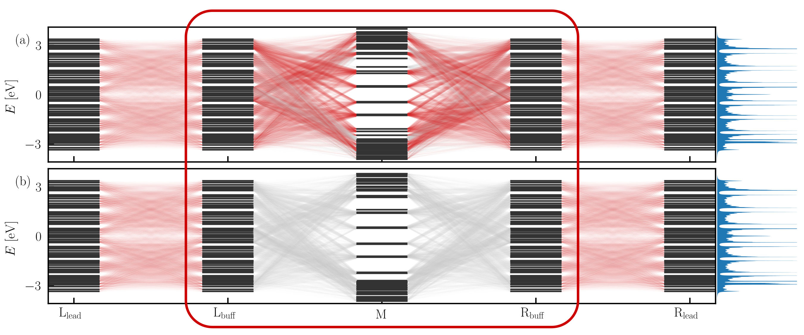
Using the coupling elements of the Hamiltonian matrix of the lead dimer , the system Hamiltonian can be extended at will by adding additional buffer and lead units . Fig. 4 shows the spectrum of the resulting Hamiltonian for the ON (upper panel) and OFF (lower panel) conformations for an exemplary system with ten buffer and ten lead units. The black horizontal lines refer to the energy levels of the different regions of the nanojunction, and the connectors between these energy levels correspond to the couplings between the pseudo-spectral states of the different regions, e.g., . It can be observed that the energy spectrum of both logical states is nearly identical. While the spectrum of the extended molecule is dense at low and at high energies, the pseudo-eigenstates of both leads are more evenly distributed and form bands at intermediate energies, with an energy spacing between the bands of . At the ordinate, the density of states (DOS) of the leads is plotted using the same Lorentzian broadening as defined by Eq. (6).
The linewidth for interstate couplings in Fig. 4 is chosen according to the strength of the respective coupling. Interestingly, when we compare the ON and OFF conformations, not only the preferred coupling channels but also the coupling strengths are very similar. To distinguish between conductive and non-conductive channels through the bridge, we introduce a measure of the connectivity asymmetry of a particular molecular channels. That is, the connectors are only colored in red if the coupling to a specific molecular channel differs by a factor of 2 at most for the largest coupling on each lead. This reveals that the majority of the extended molecule states of the ON conformation are conductive, while for the OFF conformation, nearly all states are asymmetrically coupled to the leads and therefore non-conductive. The explanation can be found by analyzing the coupling to the (nearly) degenerate pairs of extended molecule states in more detail. For each pair of states localized on the extended molecule, the coupling strength is approximately the same with both leads in the ON conformation. For the OFF logical state, one state of the doublet couples exclusively to the left while the other couples exclusively to the right lead. Thus, it can be anticipated that the OFF conformation will be significantly less conducting than the ON logical state, even without performing any dynamical simulation.
IV.2 Modeling the Time-Dependent Electronic Current
In the following, the DLvN approach is applied to investigate the electronic current in the OPE-GNR nanojunction model. A linear voltage ramp from () at to () at is chosen to drive the dynamics. At the beginning of the simulations, all subsections of the molecule are in thermal equilibrium locally. Since this is not the thermal equilibrium of the total system, an ultrafast equilibration dynamics occurs in the early stages of the simulation, as the coupling between the different parts of the nanojunction is suddenly switched on. To avoid artifacts coming from this unphysical behavior, the system is first left to equilibrate for before the bias voltage is ramped up slowly from the new initial time . Note that the Pauli principle is satisfied throughout the entire simulation for all setups investigated (cf. Sec. A of the Supporting Information for details)
Fig. 5 shows the time-evolution of the electronic current for both conformers at compared with the current voltage characteristics obtained from NEGF calculations (red curves). Regarding the NEGF reference, it can be noticed that the current gradually increases in smooth steps for the ON conformation (top and central panel of Fig. 5), while the current for the OFF logical state (bottom panel of Fig. 5) always remains very small. At all potential biases, the ON/OFF current ratio lies between and , which is in good agreement with our previous findings[54]. The finite number of states within the time-dependent DLvN simulation restricts the effective applicable bias voltages to the available lead state energies. For example, only four steps can be observed within the time-dependent current dynamics for the ON conformation (black curve in the upper panel of Fig. 5). The NEGF reference and the time-dependent results share the same qualitative features despite some marked deviations. That is, both curves describe the same few transport channels showing up at the same bias voltages.
Whenever the time-dependent bias voltage hits a resonance in a lead state, a rapid rise in conductivity is observed followed by an equilibration to a lower lying plateau. This rapid rise is observed for both the ON and OFF logical states. To understand this phenomenon, the two contributions to the current, , (cf. Eq. (22)) are plotted separately in the lower panel of Fig. 5 for the OFF configuration: the influx from the left lead as a blue and the negative outflux to the right lead () as a purple curve. As can be seen from the figure, there is either an influx or an outflux in this OFF configuration, but never both simultaneously. These dynamical features, which take place in the femtosecond time regime, can be associated with the population and depopulation of extended molecular states reacting to the new boundary conditions. Thus, those peak currents do not contribute to the overall current passing through this junction, and should be understood as an ultrafast equilibration response. This ultrafast phenomenon will be further investigated in the next chapter from the perspective of the local current.
In order to enable a more precise description of the electric current dynamics for the ON state, both leads were extended as explained above (see Eq. 15) by a certain number of tight binding units as buffer units between the central molecule and the leads and as additional lead units being coupled to the implicit electronic reservoir. While the latter allow for a higher resolution in the bias voltages and a better representation of the density of states in the leads, the former prevents the direct coupling between the central unit and the implicit electron reservoir.[59] For the ON conformation, the results for two (dark blue), five (purple), and ten (pink) lead units are shown in the upper panel of Fig. 5. It can be recognized that, with increasing number of lead units, the large jumps in between the different plateaus are gradually replaced by smoother transitions, and the curves converge slowly to reproduce the shape of the NEGF reference. Moreover, the size of the peak currents due to the ultrafast equilibration dynamics is significantly reduced due to the smaller energy gap between the states. Interestingly, simulations at higher temperatures without tight-binding extension yield similar current profiles. This is due to the smoother change in population as temperature increases, see Eq. (2).
The central panel of Fig. 5 shows the influence of introducing buffer units, i.e., lead units that are not coupled to the electronic reservoir, at the example of ten lead units with zero (black), one (dark blue), two (purple) and ten (pink) buffer units. As can be seen, introducing just a single buffer unit (dark blue curve) significantly improves the result, and by adding two or more buffer units the curve is basically converged to the NEGF reference (red curve). Interestingly, the more buffer units we introduce, the more pronounced are the features occurring when a new transport channel is opened. This phenomenon can be explained by the simple fact that increasing the number of states in the buffer implies more phases needing to equilibrate. This is a signature of the non-Markovian equilibration dynamics, an important feature of the DLvN formalism.
IV.3 Spatially-Resolved Current Dynamics
IV.3.1 Constant Bias and the Onset of Current Dynamics
An important focus of this work is the investigation of the mechanistic details of the electron transport through the OPE-GNR nanojunction. A natural choice for this analysis is the electronic current density, which provides a spatially resolved picture of the instantaneous flow of electrons. Before regarding the electron dynamics of the linear voltage ramp, let us first consider the equilibration dynamics initiated when we suddenly switch on a bias voltage of on one side of the system. Note that, as mentioned above, the system was first equilibrated for at to avoid unphysical effects coming from thermalization. Fig. 6 shows the current density dynamics for this scenario for the extended Hamiltonian using ten buffer and ten lead units. It displays the first for the OFF (cf. Fig. 6(a–d)) and the ON conformations (cf. Fig. 6(e–h)) with current coming from the left lead with (). Additionally, for the ON conformation, a dynamics in which the current comes from the right lead with (, is depicted in Fig. 6(i–l). The current voltage statistics (cf. Figs. 6(b,c), 6(f,g), and 6(j,k)) show the same prominent features as discussed in the previous section: a rapid rise in current, following a slow exponential equilibration. Recall that the curves (cf. Eq. (22)) are calculated at the boundaries between the leads and the buffer units, i.e., ten buffer units away from the extended molecule. Further positive currents are defined as flowing from the left (L) to the right side (R) of the system.

An important feature of graphene nanojunctions such as the one studied here (cf. Fig. 6), is that the current density originates from charge migration through -molecular orbitals. This is consistent with our simulations, in which the electrons flow symmetrically above and below the ZGNR plane and the current density in the molecular plane it is found to be strictly zero. After switching on the bias voltage abruptly, it takes around for the electrons to reach the boundaries of the extended molecule, i.e. the scattering region. This time delay correlates directly with the number of buffer units introduced in the tight-binding Hamiltonian. The electronic current density propagates along the bonds preferably following the central pathway. Within the next it reaches the bridge connecting the ZGNR ribbon with the central molecule. Since at that point, the current is constrained to flow along the ethynylene group, the electrons are scattered and partially reflected. The resulting backflow interferes destructively with the inflow of electrons towards the central molecule, leading to a nearly vanishing current density in that region at . Interestingly, at twice this time (), a drop in the I–V curve can be observed. This can be associated with reflected electrons arriving at the boundaries between the leads and the buffer unit, where the current is calculated. Besides, this backflow induces turbulences on the short edge (right edge) of the ZGNR ribbon. This establishes a wide stationary eddy which becomes even larger as time increases. While the current patterns on the incoming side of the lead are almost identical for ON and OFF within the first , they differ significantly at the bridge and in the outgoing lead. For the OFF conformation (cf. Fig. 6a), the route across the bridge is blocked because of the breakdown of the -conjugation. That is, a very small fraction of the current density enters the central nitrophenyl group following a turbulent circular pathway (cf. zoomed view in Fig. 6d). However, the vast majority is constantly reflected back to the incoming channel. In the later course of the dynamics (not shown), the shape of the current density patterns does not change significantly. The eddy simply becomes slightly more pronounced at first, until the current density completely vanishes at . For the ON conformation (cf. Fig. 6(e,i)), a different picture emerges. Although the electron flow is constrained by the bridge, it can reach the outgoing side already at and continues propagating towards the outgoing lead. This is facilitated by the delocalized -system through the molecular bridge.
Let us now focus on the electron dynamics on the central nitrophenyl group, and investigate the influence of the nitro group on the charge migration mechanism. While this group stands in meta position relative to the incoming flux at positive biases, (cf. Fig. 6(e–h)), it is found in ortho position for the reversed bias direction (cf. Fig. 6(i–l)). In the first moments of the scattering event at , the current densities seem to avoid the pathway along the nitro group for both polarities. This changes drastically in the following few femtoseconds, when the electron withdrawing character of the nitro group becomes apparent. Figs. 6h and 6l show enlarged views of the meta and ortho scenarios for . In the meta case, the complete electronic current density is pulled towards the side bearing the nitro group. This unilateral transport induces a backflow of the electronic current density along the opposite side of the central group. Further, a fraction of the current density is pulled towards the inner oxygen of the nitro group, where it establishes a small eddy. In the ortho case, a small share of the current density is dragged directly towards the nitro group, while the main part follows the opposite pathway along the central phenyl group and splits up again at the outlet of the central group. From here, one part is flowing to the outgoing channel, while the other part is flowing back towards the nitro group establishing an eddy at the inner oxygen – in a similar manner as in the meta case. Recall that the nitro group is a meta-directing group upon electrophilic aromatic substitutions. It now stands in a meta position with respect to the back-flowing electrons. As a consequence, a smaller amount of electronic current density is flowing towards the outgoing side of the molecule in the ortho scenario (from the right to the left lead) than in the meta case at that particular time. Interestingly, this effect persists only for a few femtoseconds and does not alter the overall current voltage characteristics after equilibration. This insightful result could be exploited to improve the nanojunction, e.g., by replacing the nitro group with an ortho-directing halide. We can hypothesize from the present simulations that this substitution could reduce the amount of current that flows back, thus reducing the turbulence through the device. It is understood that a more laminar flow of electrons is a desirable quality of a nanojunction in its ON state, as it would improve its conductivity and potentially reduce heat production.

Fig. 7 shows — with a different scaling for the colormap — the later equilibration dynamics for both scenarios starting from the last frame of Fig. 6 at . On the incoming side of the ZGNR, the magnitude of the current density rises until before it drops again. This feature is consistent with the maximum of the curve, and it coincides with a change in the transport mechanism from a central pathway towards an edge transport along the long side of the ribbon. Further, it coincides with the establishment of a specific output channel, in which the outgoing current density flows laminarly along the long edge (right edge) of the ribbon. Besides, the wide eddy established in the beginning of the dynamics on the incoming channel gets more pronounced and persists even after equilibration.
Starting from , the transport mechanism through the central group changes similarly for both current directions. Now, the electron dynamics proceeds preferably along the right side of molecular junction, independently of the position of the nitro group. The meta-directing influence of the nitro group on the transport mechanism can nonetheless be observed. When the current flows from left to right (the meta scenario), a considerable fraction of the current still flows along the nitro group side of the ring. This change in mechanism coincides with the timescale in which the magnitude of the current density on the outgoing lead steadies and reaches a magnitude comparable to the incoming one. The overall transport mechanism is almost converged at . Looking at the values of the incoming and the outgoing current at the extended molecule boundaries, we can define a quasi-stationary condition when their magnitude differ by less than . As can be seen from the insets Fig. 7c and Fig. 7f, this quasi-stationary condition is only reached at times after the potential bias was switched on. This is consistent with the picture emerging from the orbital populations, as shown in Sec. A of the ESI†.

IV.3.2 Time-Dependent Potential Bias
Fig. 8 (upper panel) shows representative snapshots of the electronic current density as streamline plots for a time-dependent potential bias. A linear voltage ramp from () at to () at (cf. Fig. 5) is applied to the ON conformation, described using a tight-binding Hamiltonian with ten buffer and ten lead units. The lower panel shows the current patterns for the same linear voltage ramp but in opposite direction (from R to L). The first frame of the time series depicted in Fig. 8 () corresponds to the same chemical potential for the influx side of the system as in the previous example and, as such, the mechanism at is very similar. That is, the current density flows laminarly along the long edges of the ZGNR ribbons and crosses the bridge on the right edge of the central group in a broad delocalized stream. Moreover, a stationary eddy on the incoming side of the junction can be observed as well. Its magnitude is too small to be seen with the colormap used in the figure. As the bias voltage increases, the preferred path of the electron dynamics changes from an edge transport to a central pathway, first on the incoming side () and subsequently () also on the outgoing side. Moreover, the stationary eddy on the short edge of the incoming side vanishes and is replaced by a transport channel following the edge down to the central group. In general for large bias voltages, most of the current density propagates along the bonds on a meandering path from the incoming to the outgoing side of the device. As can be expected from classical fluid dynamics, the current density is largest at the bottlenecks of the nanojunction, i.e., at the triple bonds connecting the leads with the nitrophenyl group. The current density remains large along the imaginary line that extends the axis spanned by these bonds until it reaches the edge of the nanoribbon. The transmission axis along the molecular junction does not align with the overall direction of the electron transport in the nanojunction. As the current density must follow this direction at the entry and exit points of the molecule, and as the momentum is very large at such high bias voltages, reflection at the ZGNR-edges most probably leads to the meandering course observed in the current dynamics.
Regarding the effect of the central group, it can be observed that the influence of the electron withdrawing increases at larger bias voltages. This can be due to the availability of a larger number of charge carriers, that react to the induction of the nitro group. For the negative bias voltage ramp (cf. Fig. 8b), the electron dynamics proceeds via its presumably preferred pathway on the right edge of the central group. The nitro group enhances this effect by concentrating the current density on one side of the phenyl group. For the positive bias voltage ramp (cf. Fig. 8a), the nitro group has the opposite effect and drags current density onto the other side of the ring. In contrast to the previous example at lower bias (cf. Fig. 7), this effect is strong enough to divert most of the current density to that side of the ring. This shows that, despite the two configurations being energetically equivalent, the nanojunction will exhibit a slight asymmetry upon reversal of the current direction.
V Conclusions
Nitro-substituted oligo(phenylene-ethynylene) covalently bound between two ZGNR electrodes is a molecular junction with great potential for nanoelectronic applications. Recently, we demonstrated using parameter-free quantum dynamical modeling that this system can be switched reliably and reversibly between two logical conformers – a planar conducting (ON) and a perpendicular less conducting conformer (OFF) – by application of a gate electric field. In the present work, we applied the driven Liouville-von-Neumann (DLvN) approach for time-dependent electronic transport calculations to investigate the electronic current dynamics in this nanojunction at different applied bias voltages. To this end, we introduced a partitioning procedure for the Hamiltonian based on the localization of orthogonal molecular orbitals obtained from a standard ground state density functional theory calculation. Here, we could show that although the resulting energy spectra are nearly identical for the ON and OFF conformers, they exhibit widely different conduction properties. This was confirmed in the subsequent time-dependent analysis, where a linear voltage ramp was applied and the current passing through the device was monitored. While in the OFF position the current through the junction always stays negligibly small, in the ON state, different transport channels are successively opened as the bias is increased. This leads to a series of distinct steps in the current voltage characteristics. In order to achieve convergence with respect to non-equilibrium Green’s function (NEGF) reference simulations, the system was extended by additional lead units using a microscopically parametrized tight binding Hamiltonian. Introducing additional units as buffer units between the lead and the extended molecule diminished further artificial coupling between the implicit electron reservoir and the extended molecule and lead to a quantitative convergence.
The mechanistic details of the charge transfer were investigated using the electronic current density, which describes the spatially resolved instantaneous flow of electrons. The first major focus of this work was the ultrafast equilibration dynamics of the incoming electronic current density, when a small bias voltage is suddenly applied. Here, it was found that the incoming electron flow exhibits typical hydrodynamic properties, where the electrons propagate through the -system mainly along the bonds, and with moderate influence of the molecular structure on ultrafast timescales. Recently, similar hydrodynamic behavior of the electronic flow has been demonstrated experimentally.[102, 103, 104]
Applying a time-dependent linear bias voltage ramp to the junction, the current density was found to follow a laminar course along the edge for small and a meandering course at large bias voltages. This curved path is caused by reflections of the current density at the ZGNR edges due to the large momentum combined with the angle between the overall direction of the electron transport and the transport axis defined by the central group. Consequently, bringing both axes into maximum coincidence could lead to an enhancement of the conductivity of the junction. This could be achieved, e.g., by choosing the same lattice direction which would lead to an armchair GNR (AGNR), or by preserving the lattice direction of the ZGNR contacts and using pyrrole rings to connect the leads with the central switching unit. This could potentially lead to an enhancement of the conductivity of the junction. Note that especially narrow AGNR are often semiconductors, and thus, not suitable as lead material. In summary, we believe that the new imaging tool presented in this work – the electronic current density – could potentially become very useful for understanding the electron transport in molecular junctions.
Acknowledgements
The authors gratefully acknowledge the Scientific Computing Services Unit of the Zentraleinrichtung für Datenverarbeitung (Zedat) at Freie Universtät Berlin for allocation of computer time. Furthermore, we thank Hans-Christian Hege for providing the ZIBAmira visualization program. The funding of the Deutsche Forschungsgemeinschaft (project TR1109/2-1 and Priority Program (SPP) 1459), from the Studienstiftung des deutschen Volkes e.V., and from the Elsa-Neumann foundation of the Land Berlin is also acknowledged. We further thank the International Max Planck Research School ”Complex Surfaces in Material Sciences” for its support.
References
- [1] M. Ratner, Nat. Nanotechnol., 2013, 8, 378–381.
- [2] L. Sun, Y. A. Diaz-Fernandez, T. A. Gschneidtner, F. Westerlund, S. Lara-Avila and K. Moth-Poulsen, Chem. Soc. Rev., 2014, 43, 7378–7411.
- [3] D. Xiang, X. Wang, C. Jia, T. Lee and X. Guo, Chem. Rev., 2016, 116, 4318–4440.
- [4] D. K. James and J. M. Tour, Molecular Wires and Electronics, Springer Science + Business Media, 2005, pp. 33–62.
- [5] Charge and Exciton Transport through Molecular Wires, ed. L. D. A. Siebbeles and F. C. Grozema, Wiley-VCH Verlag GmbH & Co. KGaA, 2011.
- [6] A. Aviram and M. A. Ratner, Chem. Phys. Lett., 1974, 29, 277–283.
- [7] C. Joachim, J. K. Gimzewski and A. Aviram, Nature, 2000, 408, 541–548.
- [8] P. Kornilovitch, A. Bratkovsky and R. S. Williams, Phys. Rev. B, 2002, 66, 165436.
- [9] R. Liu, S.-H. Ke, W. Yang and H. U. Baranger, J. Chem. Phys., 2006, 124, 024718.
- [10] I. Díez-Pérez, J. Hihath, Y. Lee, L. Yu, L. Adamska, M. A. Kozhushner, I. I. Oleynik and N. Tao, Nat. Chem., 2009, 1, 635–641.
- [11] C. A. Nijhuis, W. F. Reus and G. M. Whitesides, J. Am. Chem. Soc., 2010, 132, 18386–18401.
- [12] S. K. Yee, J. Sun, P. Darancet, T. D. Tilley, A. Majumdar, J. B. Neaton and R. A. Segalman, ACS Nano, 2011, 5, 9256–9263.
- [13] J. Hihath, C. Bruot, H. Nakamura, Y. Asai, I. Díez-Pérez, Y. Lee, L. Yu and N. Tao, ACS Nano, 2011, 5, 8331–8339.
- [14] K. Wang, J. Zhou, J. M. Hamill and B. Xu, J. Chem. Phys., 2014, 141, 054712.
- [15] J. Trasobares, D. Vuillaume, D. Théron and N. Clément, Nat. Comm., 2016, 7, 12850.
- [16] K. Wang and B. Xu, Top. Curr. Chem., 2017, 375, 17.
- [17] G. Reecht, F. Scheurer, V. Speisser, Y. J. Dappe, F. Mathevet and G. Schull, Phys. Rev. Lett., 2014, 112, 047403.
- [18] H. Yang, A. J. Mayne, G. Comtet, G. Dujardin, Y. Kuk, S. Nagarajan and A. Gourdon, Phys. Rev. B, 2014, 90, 125427.
- [19] H. P. Goswami, W. Hua, Y. Zhang, S. Mukamel and U. Harbola, J. Chem. Theory Comput., 2015, 11, 4304–4315.
- [20] K. Braun, X. Wang, A. M. Kern, H. Adler, H. Peisert, T. Chassé, D. Zhang and A. J. Meixner, Beilstein J. Nanotechnol., 2015, 6, 1100–1106.
- [21] D. Dulić, S. J. van der Molen, T. Kudernac, H. T. Jonkman, J. J. D. de Jong, T. N. Bowden, J. van Esch, B. L. Feringa and B. J. van Wees, Phys. Rev. Lett., 2003, 91, 207402–207405.
- [22] R. Pati and S. P. Karna, Phys. Rev. B, 2004, 69, 155419–155423.
- [23] J. Li, G. Speyer and O. F. Sankey, Phys. Rev. Lett., 2004, 93, 248302–248305.
- [24] P. Mendes, A. Flood and J. Stoddart, Appl. Phys. A, 2005, 80, 1197–1209.
- [25] B.-Y. Choi, S.-J. Kahng, S. Kim, H. Kim, H. W. Kim, Y. J. Song, J. Ihm and Y. Kuk, Phys. Rev. Lett., 2006, 96, 156106–156109.
- [26] M. del Valle, R. Gutiérrez, C. Tejedor and G. Cuniberti, Nat. Nanotechnol., 2007, 2, 176–179.
- [27] P. Liljeroth, J. Repp and G. Meyer, Science, 2007, 317, 1203–1206.
- [28] J. Huang, Q. Li, H. Ren, H. Su, Q. W. Shi and J. Yang, J. Chem. Phys., 2007, 127, 094705–094710.
- [29] P. Zhao, C. feng Fang, C. juan Xia, D. sheng Liu and S. jie Xie, Chem. Phys. Lett., 2008, 453, 62–67.
- [30] C. Benesch, M. F. Rode, M. Čìžek, O. Rubio-Pons, M. Thoss and A. L. Sobolewski, J. Phys. Chem. C, 2009, 113, 10315–10318.
- [31] S. Pan, Q. Fu, T. Huang, A. Zhao, B. Wang, Y. Luo, J. Yang and J. Hou, Proceedings of the National Academy of Sciences, 2009, 106, 15259–15263.
- [32] Y. Cai, A. Zhang, Y. P. Feng and C. Zhang, J. Chem. Phys., 2011, 135, 184703–184708.
- [33] D. Roldan, V. Kaliginedi, S. Cobo, V. Kolivoska, C. Bucher, W. Hong, G. Royal and T. Wandlowski, J. Am. Chem. Soc., 2013, 135, 5974–5977.
- [34] B. K. Pathem, Y. B. Zheng, S. Morton, M. Å. Petersen, Y. Zhao, C.-H. Chung, Y. Yang, L. Jensen, M. B. Nielsen and P. S. Weiss, Nano Lett., 2013, 13, 337–343.
- [35] Q.-H. Wu, P. Zhao and D.-S. Liu, Chin. Phys. Lett., 2014, 31, 057304–057307.
- [36] F. Xie, Z.-Q. Fan, K. Liu, H.-Y. Wang, J.-H. Yu and K.-Q. Chen, Org. Electron., 2015, 27, 41–45.
- [37] W. Chen, R. Chen, B. Bian, X. ao Li and L. Wang, Comput. Theor. Chem., 2015, 1067, 114–118.
- [38] T. Kumagai, Prog. Surf. Sci., 2015, 90, 239–291.
- [39] J. A. Rodríguez-Manzo, Z. J. Qi, A. Crook, J.-H. Ahn, A. T. C. Johnson and M. Drndić, ACS Nano, 2016, 10, 4004–4010.
- [40] C.-J. Xia, B.-Q. Zhang, Y.-H. Su, Z.-Y. Tu and X.-A. Yan, Optik, 2016, 127, 4774–4777.
- [41] T. Kumagai and L. Grill, Tautomerism, Wiley-Blackwell, 2016, pp. 147–174.
- [42] N. Xin, J. Wang, C. Jia, Z. Liu, X. Zhang, C. Yu, M. Li, S. Wang, Y. Gong, H. Sun, G. Zhang, Z. Liu, G. Zhang, J. Liao, D. Zhang and X. Guo, Nano Lett., 2017, 17, 856–861.
- [43] N. Fuentes, A. Martín-Lasanta, L. Á. de Cienfuegos, M. Ribagorda, A. Parra and J. M. Cuerva, Nanoscale, 2011, 3, 4003–4014.
- [44] B. K. Pathem, S. A. Claridge, Y. B. Zheng and P. S. Weiss, Annu. Rev. Phys. Chem., 2013, 64, 605–630.
- [45] M. L. Perrin, E. Burzurí and H. S. J. van der Zant, Chem. Soc. Rev., 2015, 44, 902–919.
- [46] J. L. Zhang, J. Q. Zhong, J. D. Lin, W. P. Hu, K. Wu, G. Q. Xu, A. T. S. Wee and W. Chen, Chem. Soc. Rev., 2015, 44, 2998–3022.
- [47] C. Jia, A. Migliore, N. Xin, S. Huang, J. Wang, Q. Yang, S. Wang, H. Chen, D. Wang, B. Feng, Z. Liu, G. Zhang, D.-H. Qu, H. Tian, M. A. Ratner, H. Q. Xu, A. Nitzan and X. Guo, Science, 2016, 352, 1443–1445.
- [48] C. Jia, B. Ma, N. Xin and X. Guo, Acc. Chem. Res., 2015, 48, 2565–2575.
- [49] F. Schwierz, Nat. Nanotechnol., 2010, 5, 487–496.
- [50] Z. J. Donhauser, B. A. Mantooth, K. F. Kelly, L. A. Bumm, J. D. Monnell, J. J. Stapleton, D. W. Price, A. M. Rawlett, D. L. Allara, J. M. Tour and P. S. Weiss, Science, 2001, 292, 2303–2307.
- [51] G. K. Ramachandran, Science, 2003, 300, 1413–1416.
- [52] A. M. Moore, A. A. Dameron, B. A. Mantooth, R. K. Smith, D. J. Fuchs, J. W. Ciszek, F. Maya, Y. Yao, J. M. Tour and P. S. Weiss, J. Am. Chem. Soc., 2006, 128, 1959–1967.
- [53] L. A. Agapito and H.-P. Cheng, J. Phys. Chem. C, 2007, 111, 14266–14273.
- [54] V. Pohl and J. C. Tremblay, J. Phys. Chem. C, 2016, 120, 28808–28819.
- [55] C. G. Sánchez, M. Stamenova, S. Sanvito, D. R. Bowler, A. P. Horsfield and T. N. Todorov, J. Chem. Phys., 2006, 124, 214708.
- [56] J. E. Subotnik, T. Hansen, M. A. Ratner and A. Nitzan, J. Chem. Phys., 2009, 130, 144105.
- [57] T. Zelovich, L. Kronik and O. Hod, J. Chem. Theory Comput., 2014, 10, 2927–2941.
- [58] L. Chen, T. Hansen and I. Franco, J. Phys. Chem. C, 2014, 118, 20009–20017.
- [59] T. Zelovich, L. Kronik and O. Hod, J. Chem. Theory Comput., 2015, 11, 4861–4869.
- [60] O. Hod, C. A. Rodríguez-Rosario, T. Zelovich and T. Frauenheim, J. Phys. Chem. A, 2016, 120, 3278–3285.
- [61] T. Zelovich, L. Kronik and O. Hod, J. Phys. Chem. C, 2016, 120, 15052–15062.
- [62] T. Zelovich, T. Hansen, Z.-F. Liu, J. B. Neaton, L. Kronik and O. Hod, J. Chem. Phys., 2017, 146, 092331.
- [63] U. N. Morzan, F. F. Ramírez, M. C. G. Lebrero and D. A. Scherlis, J. Chem. Phys., 2017, 146, 044110.
- [64] I. Oz, O. Hod and A. Nitzan, arXiv preprint arXiv:1810.08982, 2018.
- [65] C. D. Frisbie, Science, 2016, 352, 1394–1395.
- [66] N. Sai, N. Bushong, R. Hatcher and M. Di Ventra, Phys. Rev. B, 2007, 75, 115410.
- [67] S. Wen, S. Koo, C. Yam, X. Zheng, Y. Yan, Z. Su, K. Fan, L. Cao, W. Wang and G. Chen, J. Phys. Chem. B, 2011, 115, 5519–5525.
- [68] C. J. Páez, A. L. C. Pereira, J. N. B. Rodrigues and N. M. R. Peres, Phys. Rev. B, 2015, 92, 045426.
- [69] M. Walz, A. Bagrets and F. Evers, J. Chem. Theory Comput., 2015, 11, 5161–5176.
- [70] S. He, A. Russakoff, Y. Li and K. Varga, J. Appl. Phys., 2016, 120, 034304.
- [71] D. Nozaki and W. G. Schmidt, J. Comput. Chem., 2017, 38, 1685–1692.
- [72] M. Ernzerhof, H. Bahmann, F. Goyer, M. Zhuang and P. Rocheleau, Journal of Chemical Theory and Computation, 2006, 2, 1291–1297.
- [73] G. C. Solomon, C. Herrmann, T. Hansen, V. Mujica and M. A. Ratner, Nat. Chem., 2010, 2, 223–228.
- [74] D. Rai, O. Hod and A. Nitzan, J.Phys Chem. C, 2010, 114, 20583–20594.
- [75] J. Wilhelm, M. Walz and F. Evers, Phys. Rev. B, 2014, 89, 195406.
- [76] M. Walz, J. Wilhelm and F. Evers, Phys. Rev. Lett., 2014, 113, 136602.
- [77] J. Wilhelm, M. Walz and F. Evers, Phys. Rev. B, 2015, 92, 014405.
- [78] G. Stefanucci and C.-O. Almbladh, J. Phys. Conf. Ser., 2006, 35, 17–24.
- [79] X. Zheng, F. Wang, C. Y. Yam, Y. Mo and G. Chen, Phys. Rev. B, 2007, 75, 195127.
- [80] C. Yam, X. Zheng, G. Chen, Y. Wang, T. Frauenheim and T. A. Niehaus, Phys. Rev. B, 2011, 83, 245448.
- [81] P. Schaffhauser and S. Kümmel, Phys. Rev. B, 2016, 93, 035115.
- [82] S. Chen, Y. Kwok and G. Chen, Acc. Chem. Res., 2018, 51, 385–393.
- [83] T. M. Henderson, G. Fagas, E. Hyde and J. C. Greer, J. Chem. Phys., 2006, 125, 244104.
- [84] Z.-F. Liu and J. B. Neaton, J. Chem. Phys., 2014, 141, 131104.
- [85] L. A. Nafie, J. Phys. Chem. A, 1997, 101, 7826.
- [86] V. Pohl, G. Hermann and J. C. Tremblay, J. Comput. Chem., 2017, 38, 1515–1527.
- [87] TURBOMOLE V6.5 2013, a development of University of Karlsruhe and Forschungszentrum Karlsruhe GmbH, 1989-2007, TURBOMOLE GmbH, since 2007; available from http://www.turbomole.com (accessed Nov 20, 2016).
- [88] C. Adamo and V. Barone, J. Chem. Phys., 1999, 110, 6158–6170.
- [89] F. Weigend and R. Ahlrichs, Phys. Chem. Chem. Phys., 2005, 7, 3297–3305.
- [90] S. R. Bahn and K. W. Jacobsen, Comput. Sci. Eng., 2002, 4, 56–66.
- [91] A. H. Larsen, J. J. Mortensen, J. Blomqvist, I. E. Castelli, R. Christensen, M. Dułak, J. Friis, M. N. Groves, B. Hammer, C. Hargus, E. D. Hermes, P. C. Jennings, P. B. Jensen, J. Kermode, J. R. Kitchin, E. L. Kolsbjerg, J. Kubal, K. Kaasbjerg, S. Lysgaard, J. B. Maronsson, T. Maxson, T. Olsen, L. Pastewka, A. Peterson, C. Rostgaard, J. Schiøtz, O. Schütt, M. Strange, K. S. Thygesen, T. Vegge, L. Vilhelmsen, M. Walter, Z. Zeng and K. W. Jacobsen, J. Phys. Condens. Matter, 2017, 29, 273002.
- [92] K. S. Thygesen, M. V. Bollinger and K. W. Jacobsen, Phys. Rev. B, 2003, 67, 115404.
- [93] K. Thygesen and K. Jacobsen, Chem. Phys., 2005, 319, 111–125.
- [94] M. Strange, I. S. Kristensen, K. S. Thygesen and K. W. Jacobsen, J. Chem. Phys., 2008, 128, 114714.
- [95] J. C. Tremblay, T. Klamroth and P. Saalfrank, J. Chem. Phys., 2008, 129, 084302–084309.
- [96] J. C. Tremblay and T. Carrington Jr., J. Chem. Phys., 2004, 121, 11535–11541.
- [97] G. Hermann, V. Pohl, J. C. Tremblay, B. Paulus, H.-C. Hege and A. Schild, J. Comput. Chem., 2016, 37, 1511–1520.
- [98] G. Hermann, V. Pohl and J. C. Tremblay, J. Comput. Chem., 2017, 38, 2378–2387.
- [99] J. D. Hunter, Computing In Science & Engineering, 2007, 9, 90–95.
- [100] D. Stalling, M. Westerhoff and H.-C. Hege, The Visualization Handbook, Elsevier, 2005, pp. 749–767.
- [101] A. Kokalj, J. Mol. Graph. Model., 1999, 17, 176–179.
- [102] I. Torre, A. Tomadin, A. K. Geim and M. Polini, Phys. Rev. B, 2015, 92, 165433.
- [103] L. Levitov and G. Falkovich, Nat. Phys., 2016, 12, 672–676.
- [104] D. A. Bandurin, I. Torre, R. K. Kumar, M. B. Shalom, A. Tomadin, A. Principi, G. H. Auton, E. Khestanova, K. S. Novoselov, I. V. Grigorieva, L. A. Ponomarenko, A. K. Geim and M. Polini, Science, 2016, 351, 1055–1058.
See pages 1 of supporting.pdfSee pages 2 of supporting.pdfSee pages 3 of supporting.pdf