Defects and oxidation resilience in InSe
Abstract
We use density functional theory to study intrinsic defects and oxygen related defects in indium selenide. We find that is prone to oxidation, but however not reacting with oxygen as strongly as phosphorene. The dominant intrinsic defects in -rich material are the interstitial, a shallow donor, and the vacancy, which introduces deep traps. The latter can be passivated by oxygen, which is isoelectronic with . The dominant intrinsic defects in -rich material have comparatively higher formation energies.
I Introduction
Amongst two-dimensional materials, the families of chalcogenides such as transition metal dichalcogenides, group-III and IV monochalcogenides often offer the advantages of stability and the possibility of fabrication by epitaxial growth methods that can be scaled up—such as vapor transport epitaxy of chemical vapor deposition (CVD),[1] and chemical vapor transport.[2] Indium selenide,[3] which shares the same crystal structure with and ,[4] has recently been mechanically exfoliated into few layer flakes.[5, 6, 7] Thin flakes have been used for phase change memory devices and image sensing,[8, 9, 10] and has been suggested to be a functional material for water splitting.[11] With respect to the electronic properties, few layer has been shown to have an extraordinary electron mobility exceeding and at room and liquid-helium temperatures, in few layers, making it one of the highest known mobility 2D materials.[7, 12] This is consistent with the bulk electron mobility, which is also the highest amongst isomorphic group-III chalcogenides, according to Hall effect measurements.[13] Even though it is often -type, can also be -type and in that case it can be interesting for different purposes: It has a very high effective mass for holes near the point, where there is a ‘Mexican-hat’-type van-Hove singularity.[14, 15, 4, 16] Such a singularity gives rise to a ferromagnetic instability at low temperatures.[17] Different from other materials with ‘Mexican-hat’-type bands such as , the singularity is present in the valence band both for monolayer and for few-layer material.[16]
Thus, since both - and -type conduction regimes are of technological interest, it is desirable to be able to effectively control the type and amount of defects and impurities unintentionally introduced. and , when present, can act respectively as a shallow donor and shallow acceptor. The first is often cited as the origin of the -type conductivity. However, intrinsic shallow donors that cannot be ascribed to any impurity and disappear upon annealing have been found as well.[13, 18, 19] These were speculated to be related to deficiency.[19] According to previous theoretical calculations, adsorbed or interstitial has low formation energy in -rich material,[10] parallel to what has been found for the interstitial in ,[20] However, many studies of point defects in III-VI materials have been restricted to vacancies or substitutional type defects.[21, 22, 23, 10, 11, 24] Thus, specific defect signatures of the intrinsic shallow donors have not been assigned yet.
Interstitial atoms are supposed to increase the mechanical hardness of bulk by coupling the planar layers,[25, 26] and the same has been found for other ionized dopants as well.[27]
In addition to intrinsic defects, it is important to investigate the defects caused by the interaction with oxygen and other atmospheric contaminants. The recently achieved high mobility transistor devices were fabricated with -encapsulated layers, that were thus prevented from contact with the atmosphere.[7] Still, seems to be relatively stable in contact with air, as cleaved bulk surfaces show no signs of degradation at room temperature,[28, 29] comparing e.g. with phosphorene.
In this article, we will provide a detailed theoretical account of the properties of intrinsic defects and oxygen-related defects in . In addition, we will discuss their impact on the electronic properties of the material, in particular discussing the identity of the shallow donors in unintentionally doped .
II Methods
Parameters
The first principles calculations were performed by the density functional theory (DFT)[30, 31] implementation known as Quantum ESPRESSO.[32],11 1 version 6 All of the computations were done consistently using the following parameters. The pseudopotentials used were given by the projector augmented wave (PAW)[34, 35] approximation, and the exchange-correlation functional chosen was the generalized gradient approximation parametrized by Perdew, Burke, and Ernzerhof (GGA-PBE).[36] Specifically, the PSeudopotential Library (PSL)[37],22 2 versions 0.3.1 and 1.0.0 were used. A plane wave basis with kinetic energy cutoff of was used, and the -point samples in the Brillouin zone were calculated with the -centered Monkhorst-Pack[39] grid unless otherwise specified. Defect ionization transition levels were calculated with a -point grid of centered upon , with relaxation. All transition levels presented were at most from their values when calculated with the smaller -point grid. All geometries were relaxed to at least the default convergence thresholds (Forces ). The vacuum spacing along the -axis was six times the lattice parameter of the primitive cell of the pristine monolayer, to avoid spurious interactions. All supercells consisted of primitive unit cells.
Finally, to find the migration activation energies for the relevant defects, we also performed nudged elastic band calculations, without climbing images nor spins.
Formation Energies & Transition Levels
The formation energy of defect is given by
| (1) |
where is the energy of the supercell containing the defect, and and are the number of atoms of species and its chemical potential, respectively. The chemical potentials were evaluated both in the -rich and -rich limit. In the -rich case, the potential was obtained from the elemental material in the -, tetragonal form. The chemical potential in the -rich regime was obtained from the constraint
| (2) |
where PS is the pristine supercell. A similar definition was used to obtain the chemical potentials in the -rich limit for which we used the trigonal hP3 allotrope as reference. The chemical potential for oxygen is obtained from molecular oxygen.
The defect ionization transition levels , defined by the Fermi level at which the formation energy of the defects in charge state is the same as in charge state , were found using the marker method, which is more accurate for 2D systems due to the cancellation of systematic errors[40]. The ionization potential and electron affinity are defined by
| (3) |
The transition levels for acceptors (donors ) relative to valence band maximum (downwards from conduction band minimum ), are given by
| (4a) | ||||
| (4b) | ||||
III Results
III.1 Intrinsic Point Defects


This work considered seven intrinsic point defects (Fig. 1): the indium vacancy (VIn), the anti-site defect consisting of a selenium replacing for indium (In), indium replacing for selenium (Se), a swapped In-Se next-neighbor pair (Se-In), that we will name “swap”, the selenium vacancy VSe, selenium interstitial at the hexagonal interstitial site (ic), and above the center of the hexagonal interstitial cage (ac).
The respective band structures are represented in Fig. 2. The indium vacancy is a shallow acceptor (Fig. 2a). In has a similar band structure, but the states originating in the In vacancy are half-filled and move towards mid-gap, whereas the conduction band is little perturbed (Fig. 2b). The other anti-site defect also has semi-filled states, whereas the combined swap of neighboring and results in filled defect states near the valence band (Fig. 2c,d). The selenium vacancy introduces defect states both near the valence and conduction band (Fig. 2e). Finally, the indium interstitials are shallow donors (Fig. 2f,g). The ac configuration, the most stable (about lower in energy than the ic configuration), changes little the conduction band dispersion, however donates free holes to the conduction band states.
The formation energies as a function of the chemical potential over all available range are shown in Fig. 3. As expected, in the -rich regime the dominant defects are the vacancy and the interstitial, whereas in the -rich limit the dominant defects are the vacancy and the anti-site where replaces . These regimes will be considered in more detail in the next sections.
III.1.1 -rich regime
| Defect | ||
|---|---|---|
| VSe | ||
| VIn | ||
| –A |
crystals are typically grown using the Bridgmann method, from non-stoichiometric melts with excess, resulting in -rich crystals.[13, 18, 19]. This is expected due to the higher volatility of compared to .
In this regime, the most stable defect, of the four defects we have considered, is an interstitial above the hexagonal cage, closely followed by the vacancy, the latter of which seems to make a triangular bond between the three atoms surrounding the vacancy. Both are donors (Fig. 2), with transition levels at and above the valence band, respectively (Table 1). In particular, the interstitial, being a shallow donor, is likely to be the source of the -type conduction in this material, as previously suggested following Hall effect measurements and position lifetime experiments[19, 43, 18]. Experimentally, the defect ionization energy is , consistent with the calculations, that effectively place the transition level close to the conduction band bottom, within the method accuracy.[43] Furthermore, the experimentally observed donor center concentration is known to increase upon annealing at and the donor defects do not affect the positron lifetime, showing that it is an intrinsic defect and unlikely to be of vacancy type.[43] Focusing on the annealing, we performed a nudged elastic band calculation for both the indium interstitial and the selenium vacancy in the monolayer case, obtaining migration activation energies of about for ac and for VSe, in agreement with expectations. In addition, we note that the anti-site is energetically expensive, such that it should be rare, and does not contribute to doping. These establish that the interstitial is responsible for the -type character of undoped samples.
III.1.2 -rich regime
The two relevant intrinsic defects in this regime are the vacancy and -replacing- anti-site. VIn is a shallow acceptor, with transition levels calculated to lie below the conduction band (Table 1). However, since is placed in the inside of the layer, it is unlikely that VIn would exist on its own, without the removal of neighboring as well. is both a donor and an acceptor, with possibly a negative- level ordering (Table 1).
III.2 Physisorption

| Defect | |
|---|---|
| –A | |
| –B | |
| –C | |
| –D | |
| –E | |
| –F | |
| –G |
| Defect | |
|---|---|
| –A | |
| –B | |
| –C | |
| –D | |
| –E | |
| –F | |
| –G |
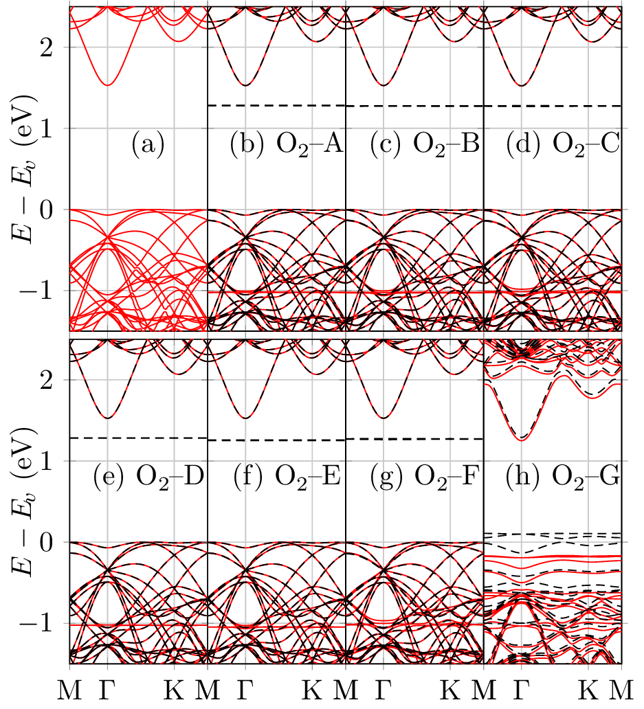
Figure 4 shows the top and side views of all the possible configurations for oxygen molecule physisorption onto . The formation energies are nearly the same (within ) for all the configurations A–F (Table 1a). The respective band structures, shown in Fig. 5, are also nearly identical, having no gap states for the majority spin and a double-degenerate empty gap state for minority spin. The coloring of the band structure plot helps reveal the deeply embedded impurity states beneath the valence band, which are flat, similar to the degenerate impurity gap states (dashed lines) in the band gap. The last of the structures considered, –G, consists of an oxygen molecule inside the interstitial cage. This is higher in energy than surface physisorbed molecules (Table 1a). Physisorbed oxygen can therefore in principle act as electron acceptor, as found in graphene,[44] phosphorene[45], and transition metal dichalcogenides[46]
III.3 Chemisorption


Chemisorption requires breaking the bond, which is found to have an energy of in our calculations, a typical overestimation, on the high side, under the PBE approximation[47] (experimentally measured to be [47]). Nevertheless, we found that the chemisorption of oxygen is energetically favorable compared to physisorption.
Figure 6 shows the top and side views of all the single oxygen atom addition defects, while the band structure plots are presented in Fig. 7. The formation energies do not depend on the and chemical potentials (Table 1b).
Table 1b shows that that there is a pair of essentially degenerate defects that are the lowest in energy. They are the –A configuration, interstitial oxygen defect between two indium atoms, near the bond-center, venturing out into the hexagonal interstitial cage, and the –B configuration, interstitial oxygen also near the bond-center between two indium atoms, but underneath the indium-selenium bond. The other defects are considerably higher in energy. The band structure plots then tell us that the three defects of this class, the lowest in energy, are basically of the same type, and that they barely differ from the band structure of the PS.
Since chemisorbed oxygen defects have no levels in the gap, their interaction with vacancies to form substitutional defects will not be of the Coulomb type but possible strain mediated, since interstitial atoms, contrary to vacancies, introduce compressing strain on the surrounding lattice. In the next section, we will consider the defects resulting of the interaction between chemisorbed oxygen and selenium vacancies.
III.4 Substitution Defects

We have considered the possibility that a lattice site is occupied by an oxygen atom or by an oxygen molecule (Fig. 1i,j). The respective band structures are shown in Fig. 2h,i. The formation energies of these defects are negative for all the range of chemical potentials, but are lowest in -rich conditions (Fig. 8). They seem to neither be donors nor acceptors, just passivating the -type selenium vacancy and reducing the band gap energy. The single substitutional oxygen atom is lower in energy than the substitutional oxygen molecule, and it is the most energetically favorable defect presented in this paper. It is especially likely to form in the presence of chalcogen vacancies,[48] through the reaction
| (5) |
which has an enthalpy balance of per oxygen atom.
IV Conclusion
We have investigated the fundamental intrinsic defects in , finding that in -rich material the anti-site is the dominant effect, whereas in -rich material the indium interstitial and selenium vacancy are the dominant defects. Our calculations suggest that the unintentional -type doping in cleanly-grown should be due to the indium interstitial, which is a shallow donor, in agreement with arguments from experiments.
Selenium vacancies have donor deep states at about above the valence band, that can partially compensate the doping by interstitials, but this state can be removed by reaction with molecular oxygen to form substitutional oxygen at the site, which has a positive energy balance of .
In the absence of intrinsic defects, oxygen chemisorption and substitution is still energetically favorable, with such defects having formation energies between and . Thus, monolayers are prone to oxidation, but still considerably stronger in resilience against the chemisorption of oxygen than that in phosphorene (the respective enthalpies for oxygen chemisorption are in and in phosphorene[49]).
We find that chemisorbed oxygen and substitutional oxygen do not have, in their most stable forms, any ionization levels in the gap. However, since chemisorbed oxygen atoms are most stable inside the layer and between In sub-layers, the structural distortion and perturbation of the charge density distribution induced by chemisorbed oxygen defects may reduce the carrier mobility, justifying the use of encapsulating layers in -based electronic devices.
Acknowledgements
This work was supported by the National Research Foundation, Prime Minister Office, Singapore, under its Medium Sized Centre Programme and CRP award “Novel 2D materials with tailored properties: beyond graphene” (Grant number R-144-000-295-281). The first-principles calculations were carried out on the CA2DM high-performance computing facilities.
References
- [1] J. Yu, J. Li, W. Zhang, and H. Chang, Chem. Sci. 6, 6705 (2015).
- [2] C.-H. Ho, 2D Mat. 3, 025019 (2016).
- [3] J. F. Sánchez-Royo, G. Muñoz-Matutano, M. Brotons-Gisbert, J. P. Martínez-Pastor, A. Segura, A. Cantarero, R. Mata, J. Canet-Ferrer, G. Tobias, E. Canadell, J. Marqués-Hueso, and B. D. Gerardot, Nano Res. 7, 1556 (2014).
- [4] V. Zólyomi, N. D. Drummond, and V. I. Fal’ko, Phys. Rev. B 89, 205416 (2014).
- [5] S. Deckoff-Jones, J. Zhang, C. E. Petoukhoff, M. K. L. Man, S. Lei, R. Vajtai, P. M. Ajayan, D. Talbayev, J. Madéo, and K. M. Dani, Sci. Rep. , 22620 (2016).
- [6] G. W. Mudd, S. A. Svatek, T. Ren, A. Patanè, O. Makarovsky, L. Eaves, P. H. Beton, Z. D. Kovalyuk, G. V. Lashkarev, Z. R. Kudrynskyi, and A. I. Dmitriev, Adv. Mat. 25, 5714 (2013).
- [7] D. A. Bandurin, A. V. Tyurnina, G. L. Yu, A. Mishchenko, V. Zólyomi, S. V. Morozov, R. K. Kumar, R. V. Gorbachev, Z. R. Kudrynskyi, S. Pezzini, Z. D. Kovalyuk, U. Zeitler, K. S. Novoselov, A. Patanè, L. Eaves, I. V. Grigorieva, V. I. Fal’ko, A. K. Geim, and Y. Cao, Nat Nano advance online publication (2016).
- [8] S. Lei, F. Wen, B. Li, Q. Wang, Y. Huang, Y. Gong, Y. He, P. Dong, J. Bellah, A. George, L. Ge, J. Lou, N. J. Halas, R. Vajtai, and P. M. Ajayan, Nano Lett. 15, 259 (2015), pMID: 25517502.
- [9] G. A. Gibson, A. Chaiken, K. Nauka, C. C. Yang, R. Davidson, A. Holden, R. Bicknell, B. S. Yeh, J. Chen, H. Liao, S. Subramanian, D. Schut, J. Jasinski, and Z. Liliental-Weber, Appl. Phys. Lett. 86, 051902 (2005).
- [10] Y. Guo and J. Robertson, arXiv preprint (2017).
- [11] Q. Peng, R. Xiong, B. Sa, J. Zhou, C. Wen, B. Wu, M. Anpo, and Z. Sun, Catal. Sci. Technol. 7, 2744 (2017).
- [12] C. Sun, H. Xiang, B. Xu, Y. Xia, J. Yin, and Z. Liu, Appl. Phys. Express 9, 035203 (2016).
- [13] A. Segura, F. Pomer, A. Cantarero, W. Krause, and A. Chevy, Phys. Rev. B 29, 5708 (1984).
- [14] S. J. Magorrian, V. Zólyomi, and V. I. Fal’ko, Phys. Rev. B 94, 245431 (2016).
- [15] D. V. Rybkovskiy, A. V. Osadchy, and E. D. Obraztsova, Phys. Rev. B 90, 235302 (2014).
- [16] G. W. Mudd, M. R. Molas, X. Chen, V. Zólyomi, K. Nogajewski, Z. R. Kudrynskyi, Z. D. Kovalyuk, G. Yusa, O. Makarovsky, L. Eaves, M. Potemski, V. I. Fal’ko, and A. Patanè, Sci. Rep. 6, 39619 (2016).
- [17] L. Seixas, A. S. Rodin, A. Carvalho, and A. H. Castro Neto, Phys. Rev. Lett. 116, 206803 (2016).
- [18] A. Segura, K. Wünstel, and A. Chevy, Appl. Phys. A 31, 139 (1983).
- [19] J. Martinez-Pastor, A. Segura, C. Julien, and A. Chevy, Phys. Rev. B 46, 4607 (1992).
- [20] H. Chen, Y. Li, L. Huang, and J. Li, RSC Adv. 5, 50883 (2015a).
- [21] Z. Rak, S. D. Mahanti, K. C. Mandal, and N. C. Fernelius, J. Phys.: Cond. Mat. 21, 015504 (2008).
- [22] Z. Rak, S. Mahanti, K. C. Mandal, and N. Fernelius, J. Phys. Chem. Solids 70, 344 (2009).
- [23] X. Li, C. Xia, X. Song, J. Du, and W. Xiong, J. Mat. Sci. 52, 7207 (2017).
- [24] H. Chen, Y. Li, L. Huang, and J. Li, J. Phys. Chem. C 119, 29148 (2015b).
- [25] K. A. Kokh, Y. M. Andreev, V. A. Svetlichnyi, G. V. Lanskii, and A. E. Kokh, Cryst. Res. Technol. 46, 327 (2011).
- [26] C. Huang, Z. Wang, Y. Ni, H. Wu, and S. Chen, RSC Adv. 7, 23486 (2017).
- [27] Z. Rak, S. D. Mahanti, K. C. Mandal, and N. C. Fernelius, Phys. Rev. B 82, 155203 (2010).
- [28] I. Miyake, T. Tanpo, and C. Tatsuyama, Jpn. J. Appl. Phys. 23, 172 (1984).
- [29] N. Balakrishnan, Z. R. Kudrynskyi, E. F. Smith, M. W. Fay, O. Makarovsky, Z. D. Kovalyuk, L. Eaves, P. H. Beton, and A. Patanè, 2D Mat. 4, 025043 (2017).
- [30] P. Hohenberg and W. Kohn, Phys. Rev. 136, B864 (1964).
- [31] W. Kohn and L. J. Sham, Phys. Rev. 140, A1133 (1965).
- [32] P. Giannozzi, S. Baroni, N. Bonini, M. Calandra, R. Car, C. Cavazzoni, D. Ceresoli, G. L. Chiarotti, M. Cococcioni, I. Dabo, A. D. Corso, S. de Gironcoli, S. Fabris, G. Fratesi, R. Gebauer, U. Gerstmann, C. Gougoussis, A. Kokalj, M. Lazzeri, L. Martin-Samos, N. Marzari, F. Mauri, R. Mazzarello, S. Paolini, A. Pasquarello, L. Paulatto, C. Sbraccia, S. Scandolo, G. Sclauzero, A. P. Seitsonen, A. Smogunov, P. Umari, and R. M. Wentzcovitch, J. Phys. C 21, 395502 (2009).
- [33] Version 6.
- [34] P. E. Blöchl, Phys. Rev. B 50, 17953 (1994).
- [35] G. Kresse and D. Joubert, Phys. Rev. B 59, 1758 (1999).
- [36] J. P. Perdew, K. Burke, and M. Ernzerhof, Phys. Rev. Lett. 77, 3865 (1996).
- [37] A. D. Corso, Comput. Mat. Sci. 95, 337 (2014).
- [38] Versions 0.3.1 and 1.0.0.
- [39] H. J. Monkhorst and J. D. Pack, Phys. Rev. B 13, 5188 (1976).
- [40] A. Carvalho and A. H. C. Neto, Phys. Rev. B 89, 081406 (2014).
- [41] L. Debbichi, O. Eriksson, and S. Lebègue, J. Phys. Chem. Lett. 6, 3098 (2015), pMID: 26267208.
- [42] D. Olguín, A. Rubio-Ponce, and A. Cantarero, Euro. Phys. J. B 86, 350 (2013).
- [43] R. M. de la Cruz, R. Pareja, A. Segura, and A. Chevy, J. Phys. C 21, 4403 (1988).
- [44] P. Giannozzi, R. Car, and G. Scoles, J. Chem. Phys. 118, 1003 (2003).
- [45] C. Han, Z. Hu, A. Carvalho, N. Guo, J. Zhang, F. Hu, D. Xiang, J. Wu, B. Lei, L. Wang, C. Zhang, A. H. C. Neto, and W. Chen, 2D Mat. 4, 021007 (2017).
- [46] P. K. Gogoi, Z. Hu, and Q. W. et al., sub. to Phys. Rev. Lett. (2017).
- [47] L. Schimka, J. Harl, and G. Kresse, J. Chem. Phys. 134, 024116 (2011).
- [48] Y. Liu, P. Stradins, and S.-H. Wei, Angewandte Chemie International Edition 55, 965 (2016).
- [49] A. Ziletti, A. Carvalho, D. K. Campbell, D. F. Coker, and A. H. Castro Neto, Phys. Rev. Lett. 114, 046801 (2015).