Imaging backscattering in graphene quantum point contacts
Abstract
We study graphene quantum point contacts (QPC) and imaging of the backscattering of the Fermi level wave function by potential introduced by a scanning probe. We consider both etched single-layer QPCs as well as the ones formed by bilayer patches deposited at the sides of the monolayer conducting channel using an atomistic tight binding approach. A computational method is developed to effectively simulate an infinite graphene plane outside the QPC using a computational box of a finite size. We demonstrate that in spite of the Klein phenomenon interference due to the backscattering at a circular n-p junction induced by the probe potential is visible in spatial maps of conductance as functions of the probe position.
I Introduction
Quantum point contacts [1, 2] (QPC) are elementary building blocks of quantum transport devices for carrier injection and read-out with control over the quantized conductance. Transport phenomena for the current injected through QPCs are studied with the spatial resolution by the scanning gate microscopy (SGM) [3] – a technique in which a charged tip of the atomic force microscope perturbs the potential within the system with the 2DEG, induces the backscattering and alters the conductance. SGM was used for graphene-based systems, the QPCs [4] states localized within the QPC [5, 6, 7], quantum Hall conditions [8, 9, 10], and magnetic focused trajectories [11, 12]. Theoretical studies for the magnetic focusing [13] and imaging snake states [14] were performed.
SGM for QPCs defined within the two-dimensional electron gas for heterostructures based on III-V semiconductors resolves interference of the incident and backscattered [15, 16, 17, 18, 19] wave functions. In graphene, a strong tip potential induces formation of a local n-p junction [20] instead of depletion of the electron gas as in III-V semiconductors. The n-p junctions in graphene are transparent for Fermi level electrons incident normally due to the Klein tunneling [21, 22, 23, 24]. Nevertheless, as we show below, the backscattering induced by the n-p junction formed by the tip induces a clear interference in SGM maps with a period of half the Fermi wavelength.
In semiconductor heterostructures with two-dimensional electron gas (2DEG), QPCs can be defined by lateral gates, which deplete the 2DEG, and thus change the constriction width and narrow the conduction channel for Fermi level electrons [2]. In graphene the channel constriction by external gates is ineffective due to Klein tunneling [25]. Etched QPCs were studied instead by both experiment [26, 27, 28, 29] and theory [30, 31, 32]. In bilayer graphene [33, 34, 35] it is possible to induce a bandgap by applying a bias between the layers [36, 37, 38]. QPCs on graphene with bilayer inclusions have been produced [10], but conductance quantization in these systems has not been theoretically investigated so far. For demonstration that the present results are independent of the QPC type we consider both etched [Fig.1(a)] and bilayer patched QPCs [Fig.1(b)]. The latter turn out less susceptible to perturbation by defects within the QPC.
In order to discuss the effects of the sample imperfections we consider both defects at the edge and within the bulk of the sample. For the edge deffects we consider singly-connected carbon atoms [39] protruding from the zigzag segments of the constriction edge that produce resonant scattering that destabilizes the conductance plateaux. For the bulk imperfections we consider local potential perturbation introduced by fluorine adatoms deposited on the surface [40].
II Theory
We use the atomistic tight-binding Hamiltionian spanned by orbitals,
| (1) |
where is the external potential at the -th site at position , and in the first term we sum over the nearest neighbors. We use the tight-binding parametrization of Ref. 41, with eV for the nearest neighbors within the same layer. For the bilayer, we take eV for the A-B dimers, eV for skew interlayer hoppings [41] between atoms of the same sublattice (A-A or B-B type), and eV for skew interlayer hopping between atoms of different sublattices. The potential energy in the lower layer is taken as the reference level , and the value of the upper layer is tuned by the electric field perpendicular to the layer. The interlayer distance is 3.32 Å.
In order to account for the effects of the lattice imperfections far from the edges of the sample we consider separate fluorine adatoms with the tight-binding parametrization of the hopping parameters taken from Ref. 40 in the dilute fluorination limit. Accordingly [40], for the hopping between the fluorine atom and the carbon ion we take eV and the on-site energy on the fluorine ion is eV.
For simulation of the SGM, we assume an effective potential of the tip with a Lorentzian form [42]
| (2) |
where are the tip coordinates, is the effective width of the tip potential, and is its maximal value ( eV unless stated otherwise).
We consider the energy range near the Dirac point. For evaluation of the transmission probability, we use the wave function matching (WFM) technique as described in Ref. 43. The transmission probability from the input lead to mode in the output lead is
| (3) |
where is the probability amplitude for the transmission from the mode in the input lead to mode in the output lead. We evaluate the conductance as , with .
| (4) |
We consider an armchair nanoribbon of width nm, 509 atoms wide. The QPC is either formed by etched out semicircles with radii nm producing a QPC [Fig. 1(a)] or by bilayer patches of the same form [Fig. 1(b)]. The QPC is nm wide in the narrowest point. We consider QPC edges with a number of singly connected atoms – similar to the ones present in the Klein edge [39, 44] [Fig. 2(c)] as well as ”clean” edges with the singly connected atoms removed [Fig. 2(d)]. For the SGM modeling, open boundary conditions (BCs) at the horizontal edges at the output QPC side are applied. We add to the right of the QPC – i.e. the output side – two leads, that are semi-infinite in the direction and extend all along the upper and lower edge of the nanoribbon [Fig. 3(c)]. The extra leads are introduced to simulate an infinite graphene sheet to eliminate the effects of the backscattering from the nanoribbon edges and the subband quantization that produces a set of subband-dependent Fermi wavelengths instead of a single one. Upon attachment of the leads, the corners of the computational box – between the right lead and the top or bottom leads [Fig. 1(c)], still act as scattering centers and produce an artificial interference.
To eliminate the scattering by the corners - which influences the SGM maps – we added in the upper-right and lower-right corners two leads that are semi-infinite in the -direction [Fig. 3] that absorb the current that has not entered the in-plane leads. The additional vertical leads are attached to the corners of the computational box as the sinks of the current. As the present approach is based on the atomistic tight-binding procedure we had to choose an atomic structure form of the leads.

III Results.
III.1 Conductance of the QPC constrictions
In Fig. 2(a,b) the transmission probability as a function of the Fermi energy is presented. A transport energy gap due to the constriction is present near the Dirac point. For QPC with singly connected atoms at the etched edge [blue line in Fig. 2(a)], the conductance exhibits a number of sharp peaks. No well developed plateaus are observed, and the conductance is much lower than the one for a uniform ribbon of the width of the narrowest part of the QPC (dashed line). This is caused by strong backscattering by the atomic-scale roughness of the etched QPC induced by the singly connected atoms. Upon their removal [cf. Fig. 2(c) and 2(d)], the conductance [the orange line in Fig. 2(a)] becomes a smooth function of the energy and approaches the maximal conductance for the QPC width.
For the bilayer patches we assume that the potential on the lower graphene layer is , and on the upper layer ( eV unless stated otherwise). For that bias within the finite size bilayer patches a bandgap is formed in the range of (0.19,0.64) eV. For the Fermi energy of the leads within gap opened by the interlayer bias in the constriction, the current doesn’t penetrate the patches [Fig. 4(a)]. For beyond the forbidden range the current flows across the patches [Fig. 4(b)]. Similar as the etched QPCs, the geometry of the QPC is specified once the sample is produced, however the bilayer-patched systems can be controlled via the electric field which allows us to turn on and off the quantizing properties, or alter the number of conducting modes in the QPC.
The conductance of the patched QPC is presented in Fig. 2(b) as a function of . The dashed line shows the conductance of a uniform nanoribbon with two rectangular bilayer patches along the entire ribbon with a width matching the conditions of the narrowest point of the QPC constriction. The conductance of the QPC with patches that contain a Klein edge and those without it, is in both cases smooth, however there is the ubiquitous backscattering that makes the conductance lower than that of the uniform ribbon of the same structure as the narrowest part of the QPC. With the singly connected atoms the dependence is smoother in the patched QPC [Fig. 2(b)] than for the etched one [Fig. 2(a)] since even for the atoms of the upper layer that have only one neighbor in-plane, there is a non-zero hopping to the atoms in the lower layer.
III.2 Simulation of the scanning gate microscopy.
For the eV, the tip introduces an n-p junction. For QPCs without the singly-connected atoms we choose the workpoint for the scanning maps at the conductance step () and at the plateau . For the etched QPC the plateau and the step are taken at eV (, see the orange point in Fig. 2(a)) and eV at the etched nanoribbon (, see the green point in Fig. 2(a)), respectively. For the patched QPC we take meV for the plateau (, the green point in Fig. 2(b)) and eV for the step (, the orange point in Fig. 2(b)).

For the QPC conductance – in the absence of the tip – the open BCs at the output side of the QPC play no significant role. The conductance is nearly the same with rigid and open BCs for the vertical edges of the ribbon. This fact results from a negligible scattering by the horizontal edges that could reverse the current back through the QPC to the input lead. However, the open conditions are crucial for the conductance mapping.
Let us first consider conductance maps for closed BCs at the upper and lower edge of the ribbon, which are then actual ends of the sample. Fig. 5(a) shows the conductance map for the etched QPC with the clean edge. The contour of the bilayer patch is marked by black solid lines. The two halos centered in the middle of QPC correspond to the tip-induced activation of the two resonances marked by orange arrows in Fig. 2(a). Away from constriction in Fig. 5(a) the conductance fluctuates in a non-regular way, due to a large number of transversal modes with different . The nanoribbon of the considered width have 19 modes at eV and 22 modes at eV. The image contains the signal of superposition of waves with many different Fermi wavelengths with the intersubband scattering.
The maps become simpler once open BCs are applied to the right (output) side of the QPC to simulate an infinite graphene halfplane. In the conductance maps for the etched QPC with open BCs [Fig. 5(b)] the QPC-centered halos remain the same as for the closed BCs [Fig. 5(a)]. The difference occurs to the right of the QPC, where the simulated flake is infinite. Far from the QPC periodic oscillations of conductance are present. Figure 6 shows the zoom at the region [dashed line in Fig. 5(b)] for the etched [Fig. 6(a)] and the patched [Fig. 6(b)] QPC. In both scans the oscillations differ by an offset and not by the oscillations period.
III.3 QPC work point vs the conductance maps
The contrast of the conductance maps for fixed parameters of the tip potential depends on the Fermi energy. The contrast grows with the absolute value of derivative. Fig. 7 and 8 present the conductance maps for open boundary conditions with the workpoints marked by the orange and light green dots on the conductance vs the Fermi energy plot in Fig. 2(a) and Fig. 2(b) of the main text, respectively. The maximal conductance value on the maps of Fig. 7 and Fig. 8 is given by the G values marked by the points on Fig. 2(a) and Fig. 2(b). The variation of the map increases with slope. The oscillation period in panels (a) and (b) of Fig. 7 and Fig. 8 changes in consistence with the value of the Fermi wavelength.
III.4 Conductance maps and edge scatterers within the constriction
The singly-connected atoms within the constrictions [Fig. 2(c-d)] are strong source of scattering for electron waves that cross the QPC. The conductance is decreased when they are present within the constriction [cf. the blue and red lines in Fig. 2]. The conductance maps for the etched QPC are given in Figures 5(b) and 9. The map changes within the constriction, but the oscillation period that is due to the backscattering at a distance from the QPC, that the paper is about, remains unchanged.

III.5 Conductance maps with bulk scatterers off the constriction
We consider the influence of scattering by strong local perturbation due to the fluorine adatoms bound to the carbon lattice at a distance from the constriction. Two adatoms are considered with the positions marked by dots in Fig. 10. We perform a modeling of scanning gate microscopy of fluorinated graphene with eV. In the conductance map we observe elliptical features near the adaomts superimposed on the conductacnce oscillation pattern with the period of half the Fermi wavelength characteristic to the clean sample. To improve the visibility of the signal, in Fig. 10(b) we plot a derivative of the conductance in Fig. 10(a). The ellipses plotted in Fig. 10 are drawn for the conditions of the interference of the wave functions incident from the QPC and backscattered by the tip and impurity, as described in the following Section.

IV Discussion.
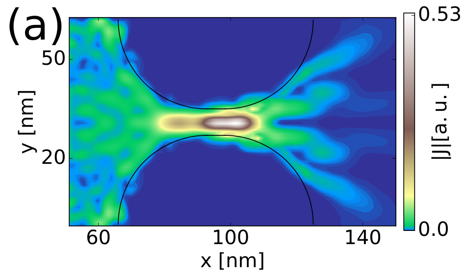
The current distribution for the etched QPC is displayed in Fig. 11 with the interference fringe pattern between the QPC and the tip that results from the tip-induced backscattering. The white circle in Fig. 11 indicates the position where the effective tip potential equals , i.e. the n-p junction. In Fig. 11(b) a zoom of the rectangle marked in Fig. 11(a) is displayed with the current orientation given by the vector map. Note that the current at the cross-section of the computational box is not necessarily conserved, as it can flow to the upper and lower contact. The current in the entire, infinite system however is always conserved. The current is focused by the circular n-p junction, and disperses to the right of it in Fig. 11(b).


(a) (b)
In the Klein tunneling effect the Fermi electron incident on a perpendicular barrier larger than is perfectly transmitted for normal incidence angle, and the transmission probability is less than 1 for other incidence angles [21, 22]. For a non-normal incidence, the current is partially reflected, and partially transmitted and refracted by the n-p-n junction [45, 46]. In Fig. 11 a normal current along the axis of the system indeed passes across the junction.The tip potential deflects the currents inside the central p conductivity region, and only the precisely normal component of the current passes through undeflected. Other incidence angles contribute to backscattering.
The angular dependence of the scattering by a circular potential in graphene has been described for an incident plane wave in Ref. [46]. In our case the wave function incoming from the QPC opening is not a plane wave but it is closer to a circular wave, which contributes to a deviation of the incidence angles from normal. Moreover, the tip potential that is of an electrostatic origin is bound to possess a smooth profile. According to Ref. [23], for smooth potential profile the transmission probability drops deep below 100% already at a low deviation of the incidence angle from normal.
Let us consider a simple model for conductance oscillations far from the QPC. The QPC is a source of a circular wave function and the SGM tip induces backscattering as argued above and shown in Fig. 12(a). The wave function incident from the QPC is partially reflected back to the opening (Fig. 12(a)). The incident wave and the wave backscattered by the tip superpose and create a standing wave between the tip and the QPC. The electron density modulation can be described by
| (5) |
This form of the scattering density gives rise to conduction map that oscillates with the tip position, with a period of , where . The Fermi vector can be calculated for low energy from the graphene linear dispersion relation [36]:
| (6) |
In Fig. 13 the cross sections along the axis of the system of Fig. 6(a) and 6(b) are shown together with a cosine shifted in phase and offset to adjust to the conductance calculated from the quantum scattering problem. Far from the QPC, the modeled conductance is close to a cosine with the that agrees with the wave vector obtained from the dispersion relation of graphene. As seen in Fig. 5(b) and Figs. 6-9, far from the QPC the oscillations can be described by a simple model. In Fig. 13 with the purple line we marked the results obtained for eV which is below . In this case no backscattered interference pattern is observed. We find that formation of the n-p junction by the tip is a necessary condition for observation of the interference fringes.
The signal observed in the presence of scattering near the fluorine adatoms with the elliptical features in the conductance map of Fig. 10 is similar to the one identified recently in III-V semiconductors [43] as due to the interference signal induced by scattering by the tip and a fixed defect. The interference paths are schematically shown in Fig. 12(b). Figure 12(a) illustrates backscattering by the n-p junction induced by the tip resulting in the interference pattern with half the flux quantum discussed above. In Fig. 12(b) the electron wave incident from the QPC to the fluorine adatom interferes with the wave that is scattered by the tip-induced n-p junction. The resulting conductance pattern can be approximately described by
| (7) |
In Fig. 10 with the dashed lines we plot the isolines of . The dashed ellipse corresponds to point-like tip, while the solid black line in Fig. 10 accounts for the finite radius of the n-p junction . The black solid line in Fig. 10 was obtained for condition . A still closer approximation is obtained when one accounts for the dependence of the penetration depth of the electron incidence angle [43]. For the blue solid line in Fig. 10 we considered the condition . Concluding, in presence of the defects the conductance map resolve the interference involving the tip, the QPC and the defect – similarly as previously described for III-V semiconductors.


The incomplete transmission in the Klein effect for electron incidence deviating from normal was used for construction of the n-p-n Fabry-Pérot interferometers [47, 48] in graphene. At n-p-n junctions [49, 50, 51, 52] interference of refracted waves in ballistic graphene appears in the scattering electron density that is referred to as the local density of states [49]. The present work deals with SGM with spatial resolution of the standing waves in conductance maps and not in the local density of states only. The present idea does not require sharp n-p junctions or a point-like injection and detection of the current as in the Veselago lensing [49, 50, 51, 52]. Fig. 14 shows the probability density without the SGM tip for the electrons incoming from the left terminal for pristine graphene (a) and with fluorine adatoms (b). For the dilute fluorinated graphene the backscattering by the fluorine adatom is resolved in the density plot in Fig. 14(b). There is no correlation between the densities and conductance maps. The SGM maps resolve the quantum transport properties or in-plane conductance of the sample when the tip becomes the source of an additional scattering. In contrast to the 2DEG in III-V quantum wells the surface electron gas in graphene can be alternatively studied with the scanning tunneling microscopy (STM) [49, 50, 51]. In this configuration the tunneling microscope acts as a contact and not as a gate electrode. Instead of the scattering effects involving the tip the STM resolves the local density of states.
Ref. 4 provided a SGM map of a graphene QPC for nominal tip potential set eV. The resistance map of this work [4] resolved only the QPC itself and not the interference fringes that were described here. The nominal value given in Ref. 4 is an unscreened parameter, and it is not granted that the screened tip potential was strong enough to induce formation of the n-p junction, since no control of was demonstrated [4]. Nevertheless, the present work indicates that observation of the spatial maps of the backscattering interference pattern in graphene is not excluded by the Klein tunelling effect.
V Summary and Conclusions
We have studied the current constriction by graphene QPCs formed by a gap between two biased bilayer patches and by a narrowing of a graphene ribbon using an atomistic tight binding method and a Landauer approach. We considered conductance mapping as a function of a floating probe position. For this purpose open boundary conditions on the output side of the QPC were introduced in order to produce an image clean from backscattering by the edges and consequences of multiple Fermi wavelengths resulting from subband quantization. With the open boundary conditions simulating an infinite graphene plane at the output side of the QPC we found a clear interference pattern in the conductance map with the period of half the Fermi wavelength characteristic to the backscattering by the tip. The interference is only observed provided that the tip induces an n-p junction in graphene. The backscattering of the electron wave function that occurs by the circular tip induced n-p junction for electron incidence at angles that deviate from normal is enough for the interference to be observed in the calculated conductance images. The finding that the Klein effect does not prevent observation of the standing waves induced by the tip in graphene opens perspectives for experimental determination of the current distribution, current branching by scattering defects, coherence length, etc.
Acknowledgments This work was supported by the National Science Centre (NCN) according to decision DEC-2015/17/B/ST3/01161. The calculations were performed on PL-Grid Infrastructure.
References
- [1] C. Beenakker and H. van Houten, Solid State Phys. 44, 1 (1991).
- [2] B. J. van Wees, H. van Houten, C. W. J. Beenakker, J. G. Williamson, L. P. Kouwenhoven, D. van der Marel, and C. T. Foxon, Phys. Rev. Lett. 60, 848 (1988).
- [3] H. Sellier, B. Hackens, M. G. Pala, F. Martins, S. Baltazar, X. Wallart, L. Desplanque, V. Bayot, and S. Huant, Semicond. Sci. Technol. 26, 064008 (2011).
- [4] S. Neubeck, L. Ponomarenko, A. Mayorov, S. Morozov, R. Yang, and K. Novoselov, Physica E 44, 1002 (2012).
- [5] M. R. Connolly, K. L. Chiu, A. Lombardo, A. Fasoli, A. C. Ferrari, D. Anderson, G. A. C. Jones, and C. G. Smith, Phys. Rev. B 83, 115441 (2011).
- [6] N. Pascher, D. Bischoff, T. Ihn, and K. Ensslin, Appl. Phys. Lett. 101, 063101 (2012).
- [7] A. G. F. Garcia, M. König, D. Goldhaber-Gordon, and K. Todd, Phys. Rev. B 87, 085446 (2013).
- [8] M. R. Connolly, R. K. Puddy, D. Logoteta, P. Marconcini, M. Roy, J. P. Griffiths, G. A. C. Jones, P. A. Maksym, M. Macucci, and C. G. Smith, Nano Lett. 12, 5448 (2012).
- [9] R. K. Rajkumar, A. Asenjo, V. Panchal, A. Manzin, Ã. Iglesias-Freire, and O. Kazakova, J. Appl. Phys. 115, 172606 (2014).
- [10] C. Chua, M. Connolly, A. Lartsev, T. Yager, S. Lara-Avila, S. Kubatkin, S. Kopylov, V. Fal’ko, R. Yakimova, R. Pearce, T. J. B. M. Janssen, A. Tzalenchuk, and C. G. Smith, Nano Lett. 14, 3369 (2014).
- [11] S. Morikawa, Z. Dou, S.-W. Wang, C. G. Smith, K. Watanabe, T. Taniguchi, S. Masubuchi, T. Machida, and M. R. Connolly, Appl. Phys. Lett. 107, 243102 (2015).
- [12] S. Bhandari, G.-H. Lee, A. Klales, K. Watanabe, T. Taniguchi, E. Heller, P. Kim, and R. M. Westervelt, Nano Lett. 16, 1690 (2016).
- [13] M. D. Petrović, S. Milovanović, and F. Peeters, Nanotechnology (2017).
- [14] K. Kolasiński, A. Mreńca-Kolasińska, and B. Szafran, Phys. Rev. B 95, 045304 (2017).
- [15] M. A. Topinka, B. J. LeRoy, R. M. Westervelt, S. E. J. Shaw, R. Fleischmann, E. J. Heller, K. D. Maranowski, and A. C. Gossard, Nature 410, 183 (2001).
- [16] B. J. LeRoy, A. C. Bleszynski, K. E. Aidala, R. M. Westervelt, A. Kalben, E. J. Heller, S. E. J. Shaw, K. D. Maranowski, and A. C. Gossard, Phys. Rev. Lett. 94, 126801 (2005).
- [17] M. P. Jura, M. A. Topinka, M. Grobis, L. N. Pfeiffer, K. W. West, and D. Goldhaber-Gordon, Phys. Rev. B 80, 041303 (2009).
- [18] N. Paradiso, S. Heun, S. Roddaro, L. Pfeiffer, K. West, L. Sorba, G. Biasiol, and F. Beltram, Physica E 42, 1038 (2010).
- [19] B. Brun, F. Martins, S. Faniel, B. Hackens, G. Bachelier, A. Cavanna, C. Ulysse, A. Ouerghi, U. Gennser, D. Mailly, S. Huant, V. Bayot, M. Sanquer, and H. Sellier, Nat. Commun. 5, 4290 (2014).
- [20] C. Gutiérrez, L. Brown, C.-J. Kim, J. Park, and P. A.P., Nat. Phys. 12, 1069 (2016).
- [21] M. I. Katsnelson, K. S. Novoselov, and A. K. Geim, Nat. Phys. 2, 620 (2006).
- [22] P. E. Allain and J. N. Fuchs, Eur. Phys. J. B 83, 301 (2011).
- [23] J. Cayssol, B. Huard, and D. Goldhaber-Gordon, Phys. Rev. B 79, 075428 (2009).
- [24] C. Schulz, R. L. Heinisch, and H. Fehske, Quantum Matter 4, 346 (2015).
- [25] R. Yang, L. Huang, Y.-C. Lai, and C. Grebogi, Phys. Rev. B 84, 035426 (2011).
- [26] Y.-M. Lin, V. Perebeinos, Z. Chen, and P. Avouris, Phys. Rev. B 78, 161409 (2008).
- [27] N. Tombros, A. Veligura, J. Junesch, M. H. D. Guimaraes, I. J. Vera-Marun, H. T. Jonkman, and B. J. van Wees, Nat. Phys. 7, 697 (2011).
- [28] B. Terrés, L. A. Chizhova, F. Libisch, J. Peiro, D. Jörger, S. Engels, A. Girschik, K. Watanabe, T. Taniguchi, S. V. Rotkin, J. Burgdörfer, and C. Stampfer, Nat. Commun. 7, 11528 (2016).
- [29] A. Kinikar, T. P. Sai, S. Bhattacharyya, A. Agarwala, T. Biswas, S. Sarker, H. R. Krishnamurthy, M. Jain, V. Shenoy, and G. A., Nat. Nano. 12, 564 (2017).
- [30] F. Muñoz Rojas, D. Jacob, J. Fernández-Rossier, and J. J. Palacios, Phys. Rev. B 74, 195417 (2006).
- [31] S. Ihnatsenka and G. Kirczenow, Phys. Rev. B 85, 121407 (2012a).
- [32] S. Ihnatsenka and G. Kirczenow, Phys. Rev. B 86, 075448 (2012b).
- [33] E. McCann and M. Koshino, Rep. Prog. Phys. 76, 056503 (2013).
- [34] E. McCann, Phys. Rev. B 74, 161403 (2006).
- [35] E. V. Castro, K. S. Novoselov, S. V. Morozov, N. M. R. Peres, J. M. B. L. dos Santos, J. Nilsson, F. Guinea, A. K. Geim, and A. H. C. Neto, Phys. Rev. Lett. 99, 216802 (2007).
- [36] A. H. Castro Neto, F. Guinea, N. M. R. Peres, K. S. Novoselov, and A. K. Geim, Rev. Mod. Phys. 81, 109 (2009).
- [37] F. Xia, D. B. Farmer, Y.-M. Lin, and P. Avouris, Nano Lett. 10, 715 (2010).
- [38] J. Park, S. B. Jo, Y.-J. Yu, Y. Kim, J. W. Yang, W. H. Lee, H. H. Kim, B. H. Hong, P. Kim, K. Cho, and K. S. Kim, Adv. Mater. 24, 407 (2012).
- [39] K. He, A. W. Robertson, S. Lee, E. Yoon, G.-D. Lee, and J. H. Warner, ACS Nano 8, 12272 (2014).
- [40] S. Irmer, T. Frank, S. Putz, M. Gmitra, D. Kochan, and J. Fabian, Phys. Rev. B 91, 115141 (2015).
- [41] B. Partoens and F. M. Peeters, Phys. Rev. B 74, 075404 (2006).
- [42] K. Kolasiński and B. Szafran, Phys. Rev. B 88, 165306 (2013).
- [43] K. Kolasiński, B. Szafran, B. Brun, and H. Sellier, Phys. Rev. B 94, 075301 (2016).
- [44] D. J. Klein and L. Bytautas, J. Phys. Chem. A 103, 5196 (1999).
- [45] G.-H. Lee, G.-H. Park, and H.-J. Lee, Nat. Phys. 11, 925 (2015).
- [46] J. Cserti, A. Pályi, and C. Péterfalvi, Phys. Rev. Lett. 99, 246801 (2007).
- [47] A. Shytov, M. Rudner, and L. Levitov, Phys. Rev. Lett. 101, 156804 (2008).
- [48] A. Young and P. Kim, Nat. Phys. 5, 222 (2009).
- [49] V. Cheianov, V. Fal’ko, and B. Altshuler, Science 315, 1252 (2007).
- [50] Y. Xing, J. Wang, and Q.-f. Sun, Phys. Rev. B 81, 165425 (2010).
- [51] A. Moghaddam and M. Zareyan, Phys. Rev. Lett. 105, 146803 (2010).
- [52] F. Libisch, H. T., R. Glattauer, L. Chizova, and J. Burgdörfer, J. Phys.: Condens. Matter 29, 114002 (2017).