Control of interlayer physics in 2H transition metal dichalcogenides
Abstract
It is assessed in detail both experimentally and theoretically how the interlayer coupling of transition metal dichalcogenides controls the electronic properties of the respective devices. Gated transition metal dichalcogenide structures show electrons and holes to either localize in individual monolayers, or delocalize beyond multiple layers - depending on the balance between spin-orbit interaction and interlayer hopping. This balance depends on layer thickness, momentum space symmetry points and applied gate fields. The design range of this balance, the effective Fermi levels and all relevant effective masses is analyzed in great detail. A good quantitative agreement of predictions and measurements of the quantum confined Stark effect in gated MoS2 systems unveils intralayer excitons as major source for the observed photoluminesence.
I Introduction
Transition metal dichalcogenides (TMDs) are expected to push nanotechnology to the ultimate scaling limit of one or a few atoms only. In contrast to graphene, these 2D materials maintain a native bandgap that is essential for most electronic device applications. TMD based devices have excellent sensitivity to external fields [1, 2, 3]. Obvious ultrascaled applications range from sensing (e.g. Refs. [4, 5, 6, 7]), lighting (e.g. Refs. [8, 9, 10]), logic devices (e.g. Refs. [11, 12]) and wearable electronics (e.g. Refs. [13, 14]).
The weak van der Waals coupling between TMD layers allows for low cost fabrication (with micro-mechanical cleavage [15]) and stacking of different TMD materials on top of each other which significantly widens the material design space [16, 17]. A critical question for most TMD systems is the nature of the coupling between TMD layers. Properties of TMD materials can be tuned via the number of coupled layers. For instance, the band-gap of MoS2 varies by about eV and switches between direct and indirect when the thickness changes [3]. These features suggested to combine TMD layers of different thicknesses and materials to improve (e.g.) tunneling field effect transistors [18, 19].
In spite of the importance of the interlayer coupling, its detailed properties and dependencies are not fully assessed, yet. For instance, recent experiments on excitons in TMD materials raised the question whether electron hole recombinations are predominantly within the same or between different TMD layers [20, 21]. Depending on the experimental setup, interlayer excitons appear in photoluminesence measurements, while intralayer transitions yield either a finite or a vanishing Stark effect [22, 23]. Given the varying findings in literature, a comparative study of experiments and realistic theoretical models is needed to conclusively assess the interlayer coupling. This is the core purpose of this work.
Although the main focus of this work is the theoretical assessment of the interlayer physics, the reliability of the theoretical answers is assessed with quantitative comparisons of predicted quantum confined Stark effects with experimental observations in various gated MoS2 structures.
All TMD devices in this work are subatomically resolved. Ab-initio electronic Hamiltonian operators are discretized with maximally localized Wannier functions (MLWF) [24]. This treatment combines numerical efficiency with the best known physical accuracy [25]. In contrast to pure ab-initio models [22], this approach allows to realistically include the presence of electric gates, thickness dependent doping and dielectric constants. Charge effects turn out to significantly influence the interlayer coupling. Commonly, electronic charge distributions are interpreted point-like within the discretization of the Poisson equation [26]. It is an important aspect of this work that these charges are resolved in subatomic resolution as well. These features guarantee full transferability of the electronic model [25, 27] to device dimensions that are computationally inaccessible to pure density functional theory (DFT) applications [28]. Note that important device aspects such as doping densities and spatially varying gate control are beyond the scope of pure DFT applications otherwise [29].
All fabricated devices of this work consist of varying numbers of TMD layers placed on SiO2 and highly p-doped Si that serves as gate electrode. Our calculations show both interlayer and intralayer excitons yield Stark effects. However, intralayer transitions are about 2 orders of magnitude less likely. Our experimental data and theoretical predictions for the Stark effect of intralayer transitions agree well. Both theory and experiments do not show significant interlayer transitions.

The paper is organized as follows. In the next section, details of the theoretical model and experimental setup are given. The results section first confirms the transferability of the electronic bandstructure model to the considered devices. It then illustrates and discusses wave function and band structure properties and their dependence on the balance of spin-orbit interaction and interlayer coupling strength. This balance depends on layer thickness, electronic momentum and applied gate fields. The comparison of calculated band gap changes with experimentally observed photoluminesence data confirms Stark effects for both inter and intra layer direct band gap excitons. In agreement with literature, intralayer excitons are found to be significantly more visible.
II Method
II.1 Experiment
The device fabrication followed the procedure of Ref. [15]. MoS2 samples were mechanically exfoliated from bulk MoS2 crystals and put on thick SiO2 layers that were grown on p-doped silicon substrates (see schematic in Fig. 1). Suitable multilayer samples were identified by optical microscopy and their thickness was confirmed independently through atomic-force microscopy. All fabricated samples were first annealed at 300 degrees Celsius to remove residue from the exfoliation process in Ar/H2 environment (800/200 SCCM). The electrostatic gates were defined through e-beam lithography on a MMA/PMMA mask, followed by 100nm deposition of Au via thermal evaporation. Next, the devices were annealed at 200 degrees Celsius (800/200 SCCM, Ar/H2) to clean the substrate of polymer residue from fabrication and improve the contact between metals and semiconductor layers before being loaded into a closed-cycle optical cryostat (Advanced Research Systems DMX-20-OM) [30] and pumped down to high vacuum at 10-7 mbar. The devices were kept at for about 6 hours in high vacuum while laser annealing was applied with a beam of a spot size. This was meant to help remove atmospheric contaminants, before the samples were cooled down to 10 K, i.e. the temperature at which all measurements were conducted. Photoluminescence measurements were performed using a continuous pump laser beam of 532 nm wavelength with a laser power of and a spot size of . The emitted light was analyzed with an Andor Shamrock Spectrograph [31] using a 150 lines/mm grating.
| u (Å) | a(Å) | c(Å) | range(Å) | |
|---|---|---|---|---|
| MoS2 | 3.12 | 3.18 | 12.48 | 20 |
| MoSe2 | 3.34 | 3.32 | 13.14 | 25 |
| WS2 | 3.15 | 3.19 | 12.49 | 23 |
| MoTe2 | 3.62 | 3.56 | 14.22 | 26 |
| WSe2 | 3.36 | 3.33 | 13.24 | 26 |
II.2 Model
The atomic structures of all TMD layers modelled in NEMO5 [32] (i.e. MoS2, WTe2, WS2, WSe2, and MoSe2) are based on relaxation calculations of the respective infinite number of layers system in trigonal prismatic polytype (i.e., in 2H symmetry) [3] performed in the DFT tool VASP [33] with the self-consistent electronic model and the convergence criterion of . A momentum mesh of 555 Monkhorst-Pack grids and energy cutoff of is used along with van der Waals force included according to Ref. [34]. The lattice constants deduced from these DFT based relaxation calculations are given in Table 1 and agree well with the findings in Ref. [35, 36]. The applied DFT model is based on the generalized gradient approximation utilizing the Perdew-Burke-Ernzerhof functionals [37]. The electronic DFT Hamiltonian is transformed into an MLWF representation using the Wannier90 software [38, 39, 40] with orbitals for the metal electrons and orbitals for the chalcogenide electrons as the initial projection. The spreading of the Wannier functions [24] is reduced iteratively until it converges to around 2 . Atom positions and their corresponding electronic Hamiltonian of finite TMD structures are then created in NEMO5 [32] as portions of the respective infinite system. As a consequence, all TMD systems in this work are intralayer periodic (in x- and y-direction of the schematic in Fig. 1) with Bloch boundary conditions applied. Nonlocal Hamiltonian elements are considered up to the material specific range listed in Table 1. All calculations of gated MoS2 structures sketched in Fig. 1 are performed with self-consistent solutions of the Schrödinger and Poisson equations. The Poisson equation is discretized on a finite element mesh (FEM). The resulting electrostatic potentials converged for FEM resolutions of or better. The electronic density resulting of the solution of the Schrödinger equation is transformed into real space simplifying the MLWF basis with Gaussian functions with =0.68 Å (in Eq. 1). This simplification eases the numerical burden during the iterative solution of the Poisson and the Schrödinger equation significantly and does not noticeably alter the actual spatial charge distribution as illustrated in Fig. 2. This figure shows the integrated charge contribution function in Eq. 2 solved with the charge distribution function of the MLWF and the fitted Gaussian function of Eq. 1, respectively.
| (1) |
| (2) |
The MoS2 thickness of the gated structure in Fig. 1 is varied between one and ten layers. In these cases, the donor doping is set to for MoS2 monolayers, for 6 MoS2 layers. The effective doping is induced from the atmospheric adsorbates. Their values are deduced from experimental threshold voltages and gate oxide capacitances [41]. The doping density is linearly interpolated for MoS2 layer systems in between 1 and 6 layers and it is assumed to be saturated for MoS2 layers thicker or equal to 6-layers [41]. As commonly done in device calculations [42], the computational burden of thick SiO2 as gate dielectric is avoided with a 12nm dielectric slab of the same equivalent capacitance in the Poisson equation. SiO2 did not enter the electron density calculations. The gate is considered as a Schottky contact with a metal work function of [43] for the highly p-doped Si. The energy offset is set to the Fermi level of the device electrons. The uncapped TMD side is considered to be exposed to vacuum, modeled with vanishing field boundary conditions for the Poisson equation. The MoS2 dielectric constant is assumed to be homogeneous but linearly varying with the layer thickness following Ref. [44]. The electronic wave functions of the conduction and the valence band states are used to solve the optical transition matrix elements. Peaks in these optical elements are considered as optical transition energies [45]. For all gate-independent bandstructures and wave function assessments in this work, a constant doping of is assumed and the Fermi level is chosen to achieve local charge neutrality for the respective systems. The electron hole recombination energies are extracted from single particle bandstructures. As discussed in Ref. [46], many particle effects are expected to have in low order no net impact on the transistion energies.


III Results
III.1 Transferability of MLWF parameters
The NEMO5-calculated bandstructures in the MLWF representation agree well with the ab-initio results of the VASP software [3] for any MoS2 layer thickness (see Fig. 3 for the monolayer and 5-layer cases). Very similar transferability of the MLWF representation and fitting procedure was found for all other TMD materials and layer thicknesses. This is remarkable, since MLWF parameterizations are sometimes created for each material thickness individually [25].


III.2 Conduction and valence band energies and masses
The conduction band minimum in 2D momentum space for monolayer and 5-layer MoS2 are shown in Figs. 4. For all TMDs considered in this work, the lowest conduction band hosts valleys at the K points and close to the Q points, respectively. Note that each K-point (Q-point) contributes to 3 (1) Brillouin zones and therefore its valley is twofold (sixfold) degenerate. Similarly, all considered TMDs show two valleys in the highest valence band at the point and at the K-point [3]. The relative energies of all these valleys depend on the layer thicknesses, as illustrated in Figs. 5 (a) and (b) for conduction and valence bands, respectively. Most of the TMDs show a transition of the conduction band minimum (valence band maximum) from K to Q (K to ) valley at around 2 layer thickness [47, 48]. The valley effective masses change with layer thickness as well (see Fig. 6) - very similar to findings of Ref. [3] for MoS2.
III.3 Band edge density of states
For a 2D system, the density of states (DOS) will be proportional to the effective mass. Note that the Q valley conduction band DOS decreases for all TMDs with increasing layer thickness as a direct consequence of the effective mass behavior. In the valence band, the valley effective masses decay with thickness, while the K valley masses stay fairly constant (see Figs. 6 (c) and (d)). The energies of K- and Q-valleys for two layer n-type TMDs are close enough so that both valleys contribute to the DOS at the band edge. Once the Q-valley of n-type TMDs (i.e., MoS2 [49], MoSe[50], WS[51]) is significantly lower in energy than the K-valley (e.g., for more than 2 layers in the case of MoS2), the DOS at the conduction band edge reduces with increasing layer thickness following the effective mass trend. This is exemplified in Fig. 7 which shows the DOS of MoS2 with varying layer thickness.


To illustrate the DOS behavior for all considered n-type (p-type) TMDs and thicknesses Fig. 8 (a) (Fig. 8 (b)) shows the effective Fermi level assuming a constant electron (hole) density of . Note that the larger the electron (hole) DOS is around the conduction band minimum (valence band maximum), the lower the effective Fermi level has to be to maintain the assumed density. All n-type TMDs except WS2 show a maximum DOS at 2 layers thickness when both K- and Q-valleys contribute. The p-type TMDs show a maximum DOS at 2 and 4 layers for MoTe2 and WSe2, respectively. This is the situation when both the and the valleys similarly contribute to the DOS around the Fermi level.
III.4 Interlayer hybridization
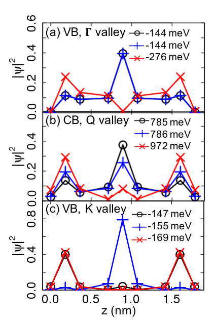
2H-phase TMDs consist of alternating layers with 2 different orientations of metal-chalcogenide bonds (differing in a 60∘ rotation) [52, 53]. If the electrons are subject to a pronounced spin-orbit interaction (e.g., in odd-layer 2H-TMD systems without inversion symmetry [53, 54, 55, 56]), electronic states spreading across alternating layers are suppressed [57, 58]. In contrast, the geometrical confinement favors electronic states that are spread across the total device if the interlayer coupling is strong enough [59]. Figure 9 shows the bandstructure of an infinite layer MoTe2 system at various symmetry points of the 2D momentum space along direction. The stronger the interlayer coupling, the stronger curved the respective bands in Fig. 9 are. In Fig. 9 several points in the bandstructure are labeled. They face different balances between the interlayer coupling strength and the spin-orbit interaction: At the valence band point (labeled with (a)), the spin-orbit interaction vanishes and only the interlayer coupling determines the shape of the electronic wave functions. Here, this coupling is significant and gives an effective mass of -2.31m0 for the top of the valence band. Consequently, the highest valence band states resemble typical infinite-barrier quantum well shapes (note they are spin degenerate, see Fig. 10 (a)). At the Q-point of the conduction band (labeled with (b) in Fig. 9) the spin-orbit interaction is finite but smaller than the strong interlayer coupling (effective mass m∗ = 0.53 m0 at Q along direction). Consequently, the shape of the electronic states shown in Fig. 10 (b) is still comparable with those of Fig. 10 (a), but the spin degeneracy is lifted. The top-valence band states at the K-point (labeled (c) in Fig. 9) face similarly strong interlayer coupling (effective mass m∗ = -1.68 at K along K-H direction) and spin-orbit interaction. Consequently, the respective wave functions avoid spreading in alternating layers. Instead, states of equivalent layers (i.e., next-nearest neighbor layers) hybridize into bonding and anti-bonding states. In the case of a 3-layer system, states of only two layers can follow that (depicted in Fig. 10 (c) with circles for the bonding state and crosses for the antibonding state), while states of the center layer (symbol ”+” in Fig. 10 (c)) are effectively isolated. In agreement with Ref. [53] the lowest conduction band states at the K-point (labeled with (d) in Fig. 9) is found to have a very small interlayer coupling (effective mass m∗ = -699m0 at K along direction), i.e., a coupling smaller than the respective spin-orbit interaction. Therefore, electronic states of individual layers barely interact and are effectively degenerate. Note that the spin-orbit interaction does not play a significant role in systems with inversion symmetry (i.e., with an even number of layers). Very small spin-orbit coupling effects observed in these systems can be addressed to small p-orbital contributions of chalcogenide atoms to the conduction band [55]. Then, wave functions are exclusively determined by the interlayer coupling strength. It is worth to emphasize that the wave function effects discussed above are found in all considered TMD materials.

III.5 Electric gate response
The effect of electric gates on TMD layers is exemplified with the absolute squared conduction band wave functions and the self-consistently solved electrostatic potential of a 6-layer gated MoS2 system shown in Figs. 11. The energies of K-valley and Q-valley states get closer with the electric field: in the field free case, the bottom of K and Q valleys are separated by more than 100 meV, whereas their energy difference is about 58 meV, as seen in Fig. 11. Higher gate fields make it energetically more favorable to avoid state delocalization across the total device. This can be seen for the Q-valley states in Fig. 11 (b) as their center shifts in the gate field direction. The electrostatic potential profiles for several different gate voltages are shown in Fig. 11 (c). In these and all other considered cases of this work, the gate field is screened within about 1 nm penetration depth. Consequently, the thinner the TMD system is, the larger is its response to the applied gate field. This is exemplified in Fig. 12 for the effective Fermi level as a function of gate bias and layer thickness. Note that the monolayer results of this figure still assume completely screened gate field in the vacuum, in spite of the pronounced penetration depth. Thus the monolayer results are given for the sake of completeness only and to ease comparison with the effective Fermi levels shown in Fig. 8. For higher gate fields and TMDs thicker than the field penetration length, the gate induced shift of effective Fermi level becomes independent of the layer thickness (see Fig. 12). Since K-valley states are localized within monolayers, they face a layer-dependent effective electric field. Accordingly, the K-valley degeneracy gets lifted by electric gates, as illustrated in Fig. 11 (a) and Fig. 13. Note that the Q-valley conduction band energies and valley valence band energies remain virtually unaffected by the electric gate (see Fig. 13).


III.6 Quantum confined Stark effect
Figure 13 also shows that the quantum confined Stark effect of the K-valley states reduces the direct band gap at the K-point. Similar effects were observed for direct band gap excitons in Ref. [23, 61] as well as in the experiments of this work: the photoluminesence peaks of direct band gap excitons show a red-shift with increasing gate voltage (see Fig. 14). Figure 14 also shows an increase of the PL amplitude with increasing gate bias. This qualitatively agrees with the bandstructure results of Fig. 13: The gate field barely changes the K-valley valence band edge, but it lowers the K-valley energy of the conduction band. This results in an increase of the K-valley electron density with the gate bias, while the K-valley hole density is approximately constant. Since the photoluminescence amplitude is approximately proportional to the product of electron and hole K-valley density (see e.g. Ref. [62, 63]), it increases with the gate bias.
It had been discussed in literature (Ref. [22, 23, 21]) whether the direct band gap excitons are recombining within individual layers or across different layers (illustrated in Fig. 15 (a)). To clarify the nature of the excitons and shed more light on this question, Fig. 15 (b) compares the field induced changes of the experimentally observed exciton energies with NEMO5 results. Since the NEMO5 calculations do not include exciton binding energies, differences of K-valley conduction and valence band states of the same layer and of maximally separated layers are used to represent intralayer and interlayer excitons, respectively. For comparability of experimental and NEMO5 results, the transition energy changes in Fig. 15 (b) are shown relative to the field free case. For both, the interlayer and intralayer transitions NEMO5 predicts a finite Stark effect, but only the intralayer transition Stark effects agree qualitatively with the experimental data. Note that NEMO5 calculations of the optical matrix elements [64] (not in the figure) showed two orders of magnitude higher probability for intralayer transitions then for interlayer ones. It is also worth to mention that our experiments did not show any Stark effect for indirect band gap excitons - in agreement with the theoretical results in Fig. 13 that show virtually gate field independent Q-valley and -valley energies. In summary, these results suggest that MoS2 excitons preferably perform intralayer transitions.
IV Conclusion
Electronic wave functions and bandstructures in 2H-TMD structures were analyzed in the MLWF representation of the nanodevice simulation tool NEMO5. Hybridization of electronic states across multiple layers was shown to depend on the balance of spin-orbit coupling and interlayer coupling strength. This balance varies strongly with the electronic momentum. Conduction band K-valley states are found to be confined in individual monolayers. In contrast, valence band K-valley states are delocalized in equivalent layers for systems with finite spin-orbit coupling or across the total device when the spin-orbit coupling disappears. This K-state hybridization can be lifted with electric gate fields. The design range of the spin-orbit interaction, the interlayer coupling, the effective Fermi levels and effective masses are carefully assessed. Experimental data of the quantum confined Stark effect of direct band gap, interlayer and intralayer exciton photoluminesence were reproduced with NEMO5. Intralayer excitons were identified as the major source for photoluminesence signals - in agreement with a previous study Ref. [23].
Acknowledgment
The work is supported by NSF EFRI-1433510. We also acknowledge the Rosen Center for Advanced Computing at Purdue University for the use of their computing resources and technical support. This research is part of the Blue Waters sustained-petascale computing project, which is supported by the National Science Foundation (award number ACI 1238993) and the state of Illinois. Blue Waters is a joint effort of the University of Illinois at Urbana-Champaign and its National Center for Supercomputing Applications. This work is also part of the “Accelerating Nano-scale Transistor Innovation with NEMO5 on Blue Waters” PRAC allocation support by the National Science Foundation (award number OCI-0832623). This work was partially supported by the National Science Foundation’s MRSEC program (DMR-1121262) and made use of its Shared Facilities at the Materials Research Center of Northwestern University. This work made use of the EPIC facility of Northwestern University’s NUANCE Center and the NUFAB facility, which have received support from the Soft and Hybrid Nanotechnology Experimental (SHyNE) Resource (NSF ECCS-1542205); the MRSEC program (NSF DMR-1121262) at the Materials Research Center; the International Institute for Nanotechnology (IIN); the Keck Foundation; and the State of Illinois. N.P.S. acknowledges support as an Alfred P. Sloan Research Fellow. J.M. acknowledges support from NSERC.
References
- [1] K. S. Novoselov, D. Jiang, F. Schedin, T. J. Booth, V. V. Khotkevich, S. V. Morozov, and A. K. Geim, Two-Dimensional Atomic Crystals, Proc. Natl. Acad. Sci. U. S. A. 102, 10451 (2005).
- [2] RadisavljevicB, RadenovicA, BrivioJ, GiacomettiV, KisA, B. Radisavljevic, A. Radenovic, J. Brivio, V. Giacometti, and A. Kis, Single-Layer MoS2 Transistors, Nat. Nanotechnol. 6, 147 (2011).
- [3] W. S. Yun, S. Han, S. C. Hong, I. G. Kim, and J. Lee, Thickness and Strain Effects on Electronic Structures of Transition Metal Dichalcogenides: 2H-MX2 Semiconductors (M = Mo, W; X = S, Se, Te), Phys. Rev. B 85, 1 (2012).
- [4] C. Zhu, D. Du, and Y. Lin, Graphene-Like 2D Nanomaterial-Based Biointerfaces for Biosensing Applications, Biosens. Bioelectron. 89, 43 (2017).
- [5] D. Jariwala, V. K. Sangwan, L. J. Lauhon, T. J. Marks, and M. C. Hersam, Emerging Device Applications for Semiconducting Two-Dimensional Transition Metal Dichalcogenides, ACS Nano 8, 1102 (2014).
- [6] K. Kalantar-zadeh and J. Z. Ou, Biosensors Based on Two-Dimensional MoS2, ACS Sensors 1, 5 (2016).
- [7] M. R. Esmaeili-Rad and S. Salahuddin, High Performance Molybdenum Disulfide Amorphous Silicon Heterojunction Photodetector, Sci. Rep. 3, 2345 (2013).
- [8] J. S. Ross, P. Klement, A. M. Jones, N. J. Ghimire, J. Yan, M. G., T. Taniguchi, K. Watanabe, K. Kitamura, W. Yao, D. H. Cobden, and X. Xu, Electrically Tunable Excitonic Light-Emitting Diodes Based on Monolayer WSe2 p-n Junctions, Nat. Nano 9, 268 (2014).
- [9] M. S. Choi, D. Qu, D. Lee, X. Liu, K. Watanabe, T. Taniguchi, and W. J. Yoo, Lateral MoS2 p-n Junction Formed by Chemical Doping for Use in High-Performance Optoelectronics, ACS Nano 8, 9332 (2014).
- [10] F. Withers, O. Del Pozo-Zamudio, A. Mishchenko, a. P. Rooney, A. Gholinia, K. Watanabe, T. Taniguchi, S. J. Haigh, a. K. Geim, a. I. Tartakovskii, and K. S. Novoselov, Light-emitting Diodes by Band-Structure Engineering in van der Waals Heterostructures, Nat. Mater. 14, 301 (2015).
- [11] S. Bertolazzi, D. Krasnozhon, and A. Kis, Nonvolatile Memory Cells Based on MoS2/Graphene Heterostructures, ACS Nano 7, 3246 (2013).
- [12] V. K. Sangwan, D. Jariwala, I. S. Kim, K.-S. Chen, T. J. Marks, L. J. Lauhon, and M. C. Hersam, Gate-Tunable Memristive Phenomena Mediated by Grain Boundaries in Single-Layer MoS2, Nat. Nanotechnol. 10, 403 (2015).
- [13] Z. Q. Zheng, T. M. Zhang, J. D. Yao, Y. Zhang, J. R. Xu, and G. W. Yang, Flexible, Transparent and Ultra-Broadband Photodetector Based on Large-Area WSe2 Film for Wearable Devices, Nanotechnology 27, 11 (2016).
- [14] J. Y. Oh, J. H. Lee, S. W. Han, S. S. Chae, E. J. Bae, Y. H. Kang, W. J. Choi, S. Y. Cho, J.-O. Lee, H. K. Baik, and T. I. Lee, Chemically Exfoliated Transition Metal Dichalcogenide Nanosheet-Based Wearable Thermoelectric Generators, Energy Environ. Sci. 9, 1696 (2016).
- [15] F. Bonaccorso, A. Lombardo, T. Hasan, Z. Sun, L. Colombo, and A. C. Ferrari, Production, Processing and Placement of Graphene and Two Dimensional Crystals, Mater. Today , 564 (2012).
- [16] L. Britnell, R. M. Ribeiro, A. Eckmann, R. Jalil, B. D. Belle, A. Mishchenko, Y.-J. Kim, R. V. Gorbachev, T. Georgiou, S. V. Morozov, A. N. Grigorenko, A. K. Geim, C. Casiraghi, A. H. C. Neto, and K. S. Novoselov, STrong Light-Matter Interactions in Heterostructures of Atomically Thin Films, Science 340, 1311 (2013).
- [17] A. K. Geim and I. V. Grigorieva, Van der Waals Heterostructures, Nature 499, 419 (2014).
- [18] S. L. Howell, D. Jariwala, C. C. Wu, K. S. Chen, V. K. Sangwan, J. Kang, T. J. Marks, M. C. Hersam, and L. J. Lauhon, Investigation of Band-Offsets at Monolayer-Multilayer MoS2 Junctions by Scanning Photocurrent Microscopy, Nano Lett. 15, 2278 (2015).
- [19] F. W. Chen, H. Ilatikhameneh, T. A. Ameen, G. Klimeck, and R. Rahman, Thickness engineered tunnel field-effect transistors based on phosphorene, IEEE Electron Device Lett. 38, 130 (2017).
- [20] X. Zhu, N. R. Monahan, Z. Gong, H. Zhu, K. W. Williams, and C. A. Nelson, Charge Transfer Excitons at van der Waals Interfaces, J. Am. Chem. Soc. 137, 8313 (2015).
- [21] H. Chen, X. Wen, J. Zhang, T. Wu, Y. Gong, X. Zhang, J. Yuan, C. Yi, J. Lou, P. M. Ajayan, W. Zhuang, G. Zhang, and J. Zheng, Ultrafast Formation of Interlayer Hot Excitons in Atomically Thin MoS2/WS2 Heterostructures, Nat. Commun. 7, 12512 (2016).
- [22] T. Chu, H. Ilatikhameneh, G. Klimeck, R. Rahman, and Z. Chen, Electrically Tunable Bandgaps in Bilayer MoS2, Nano Lett. 15, 8000 (2015).
- [23] J. Klein, J. Wierzbowski, A. Regler, J. Becker, F. Heimbach, K. Müller, M. Kaniber, and J. J. Finley, Stark Effect Spectroscopy of Mono- and Few-Layer MoS2, Nano Lett. 16, 1554 (2016).
- [24] N. Marzari, A. A. Mostofi, J. R. Yates, I. Souza, and D. Vanderbilt, Maximally Localized Wannier Functions: Theory and Applications, Rev. Mod. Phys. 84, 1419 (2012).
- [25] Á. Szabó, R. Rhyner, and M. Luisier, Ab initio Simulation of Single- and Few-Layer MoS2 Transistors: Effect of Electron-Phonon Scattering, Phys. Rev. B - Condens. Matter Mater. Phys. 92, 1 (2015).
- [26] H. Ilatikhameneh, Y. Tan, B. Novakovic, G. Klimeck, R. Rahman, and J. Appenzeller, Tunnel Field-Effect Transistors in 2-D Transition Metal Dichalcogenide Materials, IEEE J. Explor. Solid-State Computat. Devices Circuits 1, 12 (2015).
- [27] S. Fang, R. Kuate Defo, S. N. Shirodkar, S. Lieu, G. A. Tritsaris, and E. Kaxiras, Ab Initio Tight-Binding Hamiltonian for Transition Metal Dichalcogenides, Phys. Rev. B - Condens. Matter Mater. Phys. 92, 205108 (2015).
- [28] J. Maassen, M. Harb, V. Michaud-Rioux, Y. Zhu, and H. Guo, Quantum Transport Modeling from First Principles, Proc. IEEE 101, 518 (2013).
- [29] http://cms.mpi.univie.ac.at/vasp/vasp.pdf, (2015).
- [30] http://www.arscryo.com/CS204_F-DMX-20-OM.html, (2016a).
- [31] http://www.andor.com/spectrograph/shamrock-spectrograph-series/shamrock-303i, (2016b).
- [32] S. Steiger, M. Povolotskyi, H. H. Park, T. Kubis, and G. Klimeck, NEMO5: A parallel Multiscale Nanoelectronics Modeling Tool, IEEE Trans. Nanotechnol. 10, 1464 (2011).
- [33] G. Kresse and J. Furthmüller, Efficient Iterative Schemes for ab Initio Total-Energy Calculations Using a Plane-Wave Basis Set, Phys. Rev. B 54, 11169 (1996).
- [34] T. Bučko, J. Hafner, S. Lebègue, and J. G. Ángyán, Improved Description of the Structure of Molecular and Layered Crystals: Ab Initio DFT Calculations with van der Waals Corrections, J. Phys. Chem. A 114, 11814 (2010).
- [35] F. Jellinek, G. Brauer, and H. Müller, Molybdenum and Niobium Sulphides, Nature 185, 376 (1960).
- [36] W. Wei, Y. Dai, C. Niu, and B. Huang, Controlling the Electronic Structures and Properties of in-Plane Transition-Metal Dichalcogenides Quantum Wells, Sci. Rep. 5, 17578 EP (2015).
- [37] J. P. Perdew, K. Burke, and Y. Wang, Generalized Gradient Approximation for the Exchange-Correlation Hole of a Many-Electron System, Phys. Rev. B 54, 16533 (1996).
- [38] N. Marzari and D. Vanderbilt, Maximally-Localized Generalized Wannier Functions for Composite Energy Bands, Phys. Rev. B 56, 12847 (1997).
- [39] K. S. Thygesen, L. B. Hansen, and K. W. Jacobsen, Partly wccupied wannier functions: Construction and applications, Phys. Rev. B 72, 125119 (2005).
- [40] R. Das, S. K. Pandey, and P. Mahadevan, Layer dependent electronic structure changes in transition metal dichalcogenides-The role of geometric confinement, , 1 (2017).
- [41] D. Jariwala, V. K. Sangwan, D. J. Late, J. E. Johns, V. P. Dravid, T. J. Marks, L. J. Lauhon, and M. C. Hersam, Band-Like Transport in High Mobility Unencapsulated Single-Layer MoS2 Transistors, Appl. Phys. Lett. 102, 173107 (2013).
- [42] S. Saito, K. Torii, M. Hiratani, and T. Onai, Analytical Quantum Mechanical Model for Accumulation Capacitance of MOS Structures, IEEE Electron Device Lett. 23, 348 (2002).
- [43] A. Novikov, Experimental Measurement of Work Function in Doped Silicon Surfaces, Solid. State. Electron. 54, 8 (2010).
- [44] X. Chen, Z. Wu, S. Xu, L. Wang, R. Huang, Y. Han, W. Ye, W. Xiong, T. Han, G. Long, Y. Wang, Y. He, Y. Cai, P. Sheng, and N. Wang, Probing the Electron States and Metal-Insulator Transition Mechanisms in Molybdenum Disulphide Vertical Heterostructures, Nat. Commun. 6, 6088 (2015).
- [45] P. Sarangapani, D. Mejia, J. Charles, W. Gilbertson, H. Ilatikhameneh, T. Ameen, A. Roche, J. Fonseca, and G. Klimeck, in 2015 Int. Work. Comput. Electron. (2015) pp. 1–3.
- [46] K. Liu, L. Zhang, T. Cao, C. Jin, D. Qiu, Q. Zhou, A. Zettl, P. Yang, S. G. Louie, and F. Wang, Evolution of interlayer coupling in twisted molybdenum disulfide bilayers, Nat. Commun. 5, 1 (1).
- [47] L. Zhang and A. Zunger, Evolution of electronic structure as a function of layer thickness in group-VIB transition metal dichalcogenides: Emergence of localization prototypes, Nano Letters 15, 949 (2015).
- [48] J. Kang, L. Zhang, and S. H. Wei, A Unified Understanding of the Thickness-Dependent Bandgap Transition in Hexagonal Two-Dimensional Semiconductors, Journal of Physical Chemistry Letters 7, 597 (2016).
- [49] H.-M. Li, D. Lee, D. Qu, X. Liu, J. Ryu, A. Seabaugh, and W. J. Yoo, Ultimate Thin Vertical p-n Junction Composed of Two-Dimensional Layered Molybdenum Disulfide. Nat. Commun. 6, 6564 (2015).
- [50] Y. Jin, D. H. Keum, S. J. An, J. Kim, H. S. Lee, and Y. H. Lee, A Van der Waals Homojunction: Ideal p-n Diode Behavior in MoSe2, Adv. Mater. 27, 5534 (2015).
- [51] D. Ovchinnikov, A. Allain, Y. S. Huang, D. Dumcenco, and A. Kis, Electrical Transport Properties of Single-Layer WS2, ACS Nano 8, 8174 (2014).
- [52] J. Wilson and A. Yoffe, The Transition Metal Dichalcogenides Discussion and Interpretation of the Observed Optical, Electrical and Structural Properties, Adv. Phys. 18, 193 (1969).
- [53] R. Akashi, M. Ochi, S. Bordács, R. Suzuki, Y. Tokura, Y. Iwasa, and R. Arita, Two-Dimensional Valley Electrons and Excitons in Noncentrosymmetric , Phys. Rev. Applied 4, 014002 (2015).
- [54] Y. Li, Y. Rao, K. F. Mak, Y. You, S. Wang, C. R. Dean, and T. F. Heinz, Probing Symmetry Properties of Few-Layer MoS2 and h-BN by Optical Second-Harmonic Generation, Nano Lett. , 3329 (2013).
- [55] K. Komider, J. W. González, and J. Fernández-Rossier, Large Spin Splitting in the Conduction Band of Transition Metal Dichalcogenide Monolayers, Phys. Rev. B - Condens. Matter Mater. Phys. 88, 1 (2013).
- [56] J. R. Schaibley, H. Yu, G. Clark, P. Rivera, J. S. Ross, K. L. Seyler, W. Yao, and X. Xu, Valleytronics in 2D Materials, Nat. Rev. Mater. 1, 16055 (2016).
- [57] A. M. Jones, H. Yu, J. S. Ross, P. Klement, N. J. Ghimire, J. Yan, D. G. Mandrus, W. Yao, and X. Xu, Spin-Layer Locking Effects in Optical Orientation of Exciton Spin in Bilayer WSe2, Nat. Phys. 10, 130 (2014).
- [58] Z. Gong, G.-b. Liu, H. Yu, D. Xiao, X. Cui, X. Xu, and W. Yao, Magnetoelectric Effects and Valley-Controlled Spin Quantum Gates in Transition Metal Dichalcogenide Bilayers, Nat. Commun. 4, 2053 (2013).
- [59] X. Xu, W. Yao, D. Xiao, and T. F. Heinz, Spin and Pseudospins in Layered Transition Metal Dichalcogenides, Nat. Phys. 10, 343 (2014).
- [60] K. F. Mak, C. Lee, J. Hone, J. Shan, and T. F. Heinz, Atomically thin MoS2: A new direct-gap semiconductor, Phys. Rev. Lett. 105, 2 (2010).
- [61] J. G. Kim, W. S. Yun, S. Jo, J. Lee, and C.-h. Cho, Effect of Interlayer Interactions on Exciton Luminescence in Atomic-Layered MoS2 Crystals, Sci. Rep. , 1 (2016).
- [62] J. Piprek, Efficiency droop in nitride-based light-emitting diodes, Physica Status Solidi (A) Applications and Materials Science 207, 2217 (2010).
- [63] R. N. Hall, Electron-hole recombination in germanium, Phys. Rev. 87, 387 (1952).
- [64] S. L. Chuang, Physics of Optoelectronic Devices, Wiley Series in Pure and Applied Optics (Wiley, 1995).