Direct cavity detection of Majorana pairs
Abstract
No experiment could directly test the particle/antiparticle duality of Majorana fermions, so far. However, this property represents a necessary ingredient towards the realization of topological quantum computing schemes. Here, we show how to complete this task by using microwave techniques. The direct coupling between a pair of overlapping Majorana bound states and the electric field from a microwave cavity is extremely difficult to detect due to the self-adjoint character of Majorana fermions which forbids direct energy exchanges with the cavity. We show theoretically how this problem can be circumvented by using photo-assisted tunneling to fermionic reservoirs. The absence of direct microwave transition inside the Majorana pair in spite of the light-Majorana coupling would represent a smoking gun for the Majorana self-adjoint character.
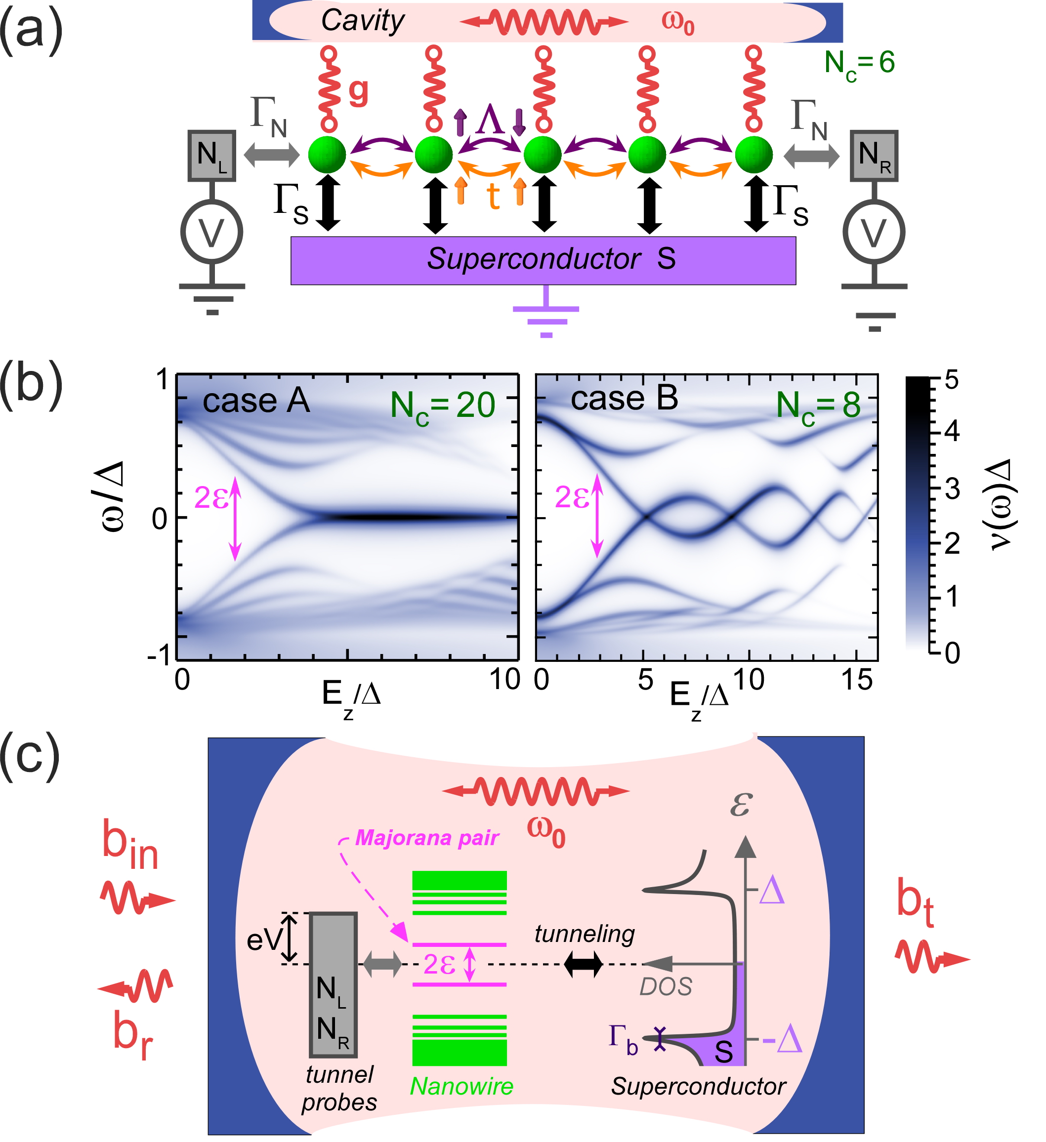
Majorana quasiparticles are among the most intriguing excitations predicted in condensed matter physics[1]. The Majorana particle is equal to its own antiparticle, a property which opens up possibilities of non-abelian statistics[2] and topologically protected quantum computation[3] in condensed matter systems. Low frequency conductance measurements have prevailed so far in the experimental search for these exotic quasiparticles. In particular, hybrid structures combining semiconducting nanowires and superconductors have been intensively investigated[4, 5]. The recent observation of zero energy conductance peaks and pairs of peaks with an oscillatory splitting are consistent with the existence of Majorana bound states (MBSs)[6, 7, 8, 9, 12, 10]. However, it is essential to find new tools to test more specifically the nature of these peaks[13, 14, 15, 16, 17, 18].
Paradoxically, the self-adjoint character of MBSs, which draws so much interest, also makes them very difficult to detect. Photons trapped in a high finesse cavity are a priori very appealing for probing these elusive excitations[19]. Indeed, light, contrarily to conductance measurements, preserves the occupation number encoded into a pair of MBSs. Unfortunately, for the same reason, a pair of MBSs cannot exchange energy with an electromagnetic field, which forbids any direct spectroscopy. This seems to limit the use of light in complex setups[20, 22, 21, 23, 25, 24]. Recently proposed quantum computing architectures rely on an indirect MBSs-photon coupling through a metallic Josephson circuit[26, 27, 28, 29, 30, 31, 32, 33, 34].
In this theoretical work, we show that the imperfections of a realistic Majorana nanocircuit, although undesirable for quantum information applications, can be exploited at present to characterize MBSs with microwave techniques. First, a realistic Majorana nanocircuit must have a finite size to remain in the coherent regime. Therefore, MBSs can have a spatial overlap. This naturally generates, for a pair of MBSs, an energy splitting and a direct coupling to the cavity electric field[21, 35]. Second, the presence of even a tiny amount of zero-energy quasiparticles in superconducting or normal metal contacts, which is inherent to experimental setups demonstrated so far, switches on photo-assisted tunnel processes which involve only one partner of a Majorana doublet. During these transitions, photons with frequency are exchanged between the cavity and the Majorana pair, with a rate set by . However, transitions at frequency remain forbidden regardless of the circuit parameters. The purely longitudinal nature of , thereby revealed, would represent a direct signature, in the simplest setup, of the self adjoint-character of MBSs.
Hybrid nanocircuits with superconducting parts have been coupled very recently to microwave cavities[36, 37, 38, 39]. The light/matter coupling in such devices can be described generically with the Hamiltonian
| (1) |
with the cavity frequency. In a typical experiment, one determines the cavity frequency pull and damping pull from the cavity microwave response measured at frequency . In case of an electric coupling scheme, from a semiclassical linear response description, these signals correspond to , with the nanocircuit charge susceptibility[37]. In a first approach, one can assume that the nanocircuit spectrum is discrete. Since are quadratic, one can use and , with , Bogoliubov operators which combine electron and hole excitations, and matrix elements which depend on the overlap of the cavity photonic pseudopotential with the wavefunctions associated to [35]. At zero temperature (), this gives . Importantly, due to the Pauli exclusion principle, one has . Hence, does not involve transitions between electron and holes associated to conjugated operators and . This selection rule can be extended to or a level broadening smaller than the inter-level separation[40]. However, having a nanocircuit response at is possible provided there exists a state degeneracy in the nanocircuit[40], as observed in spin-degenerate superconducting atomic contacts[36, 41]. In contrast, lifting degeneracies is crucial to obtain MBSs. In elementary models[4, 5], when a finite portion of nanoconductor is driven to its topological phase, one non-degenerate Bogoliubov doublet () approaches alone the zero energy area to form a pair of MBSs described by self-adjoint creation operators and such that one has, at low energies, with . An important signature of this scenario is the absence of direct microwave transitions in the Majorana subspace, i.e. due to . Remarkably, this occurs even when the Majorana-cavity coupling is finite, i.e. contains a term in with . Using a spin analogy, the cavity and the MBSs can only have a longitudinal coupling, which is not able to change the state of the Majorana pair, i.e. and are represented by collinear vectors in the Bloch sphere associated to the Majorana subspace. This gives a smoking gun for the non-degenerate electron-hole conjugated pair, or equivalently, the pair of self-adjoint excitations (, ). Importantly, the absence of direct microwave transitions in the Majorana doublet is meaningful only if one can confirm . Furthermore, the absence of direct transitions should be robust when the control parameters of the nanocircuit are varied, to discard any accidental cancellation of . We use below a specific example to show how these tasks can be achieved.
We now consider a semiconducting nanowire subject to spin-orbit coupling and a Zeeman field. The nanowire is tunnel coupled along its whole length to a superconducting contact . It is also coupled at both ends to normal metal contacts and which enable the measurement of the nanowire density of states . We describe this circuit with a phenomenological one-dimensional tight-binding chain with and the creation operator for an electron with spin in site of the chain (Fig.1a). We denote by the Zeeman field on the sites, the sites chemical potential, which can be tuned with a gate voltage, the hoping constant between the sites and the spin-orbit constant. So far, studies on MBSs coupled to cavities have reduced the effect of to an effective pairing term added to [20, 22, 21, 23]. However, a realistic model must also take into account level broadening and dissipation. Therefore, we describe explicitly tunneling to and with an Hamiltonian (see [40] for details). This leads us to introduce the tunnel rate between site and contact and the tunnel rate between site and contact . The DOS of depends on the superconducting gap but also on a phenomenological parameter which accounts for a broadening of the BCS peaks and a finite low energy DOS (Fig.1c). Such effects can be caused by a finite magnetic field[42, 43]. We consider short chains and choose parameters such that few subgap levels are visible in the DOS of the nanowire, like in recent experiments[12, 10]. More precisely, for case A, one has , , , , , and for case B one has , , , , , . We use , and for both cases. The density of states at the ends of the nanowire reveals the occurrence of a pair of MBSs above a critical Zeeman field (Fig. 1b). These MBSs show an oscillatory energy splitting with and for a very short chain (case B), or stick to zero energy for a longer chain (case A)[11].
We assume that the above nanocircuit is embedded in a microwave cavity. Hence, we use Hamiltonian of Eq.(1) with and . This last term means that cavity photons modulate the chemical potential of site with a coupling constant [35]. To treat on the same footing internal nanowire transitions and tunneling to the reservoirs, we use a Keldysh approach[41, 44, 45, 46, 37]. We use Python and Numba, a LLVM-based Python compiler[47], to calculate numerically with[37]
| (2) |
and . Above, the retarded and advanced multisite Green’s functions and the lesser self energy can be calculated from , while takes into account the structure of the photon/particle coupling in the Nambuspin space [40].
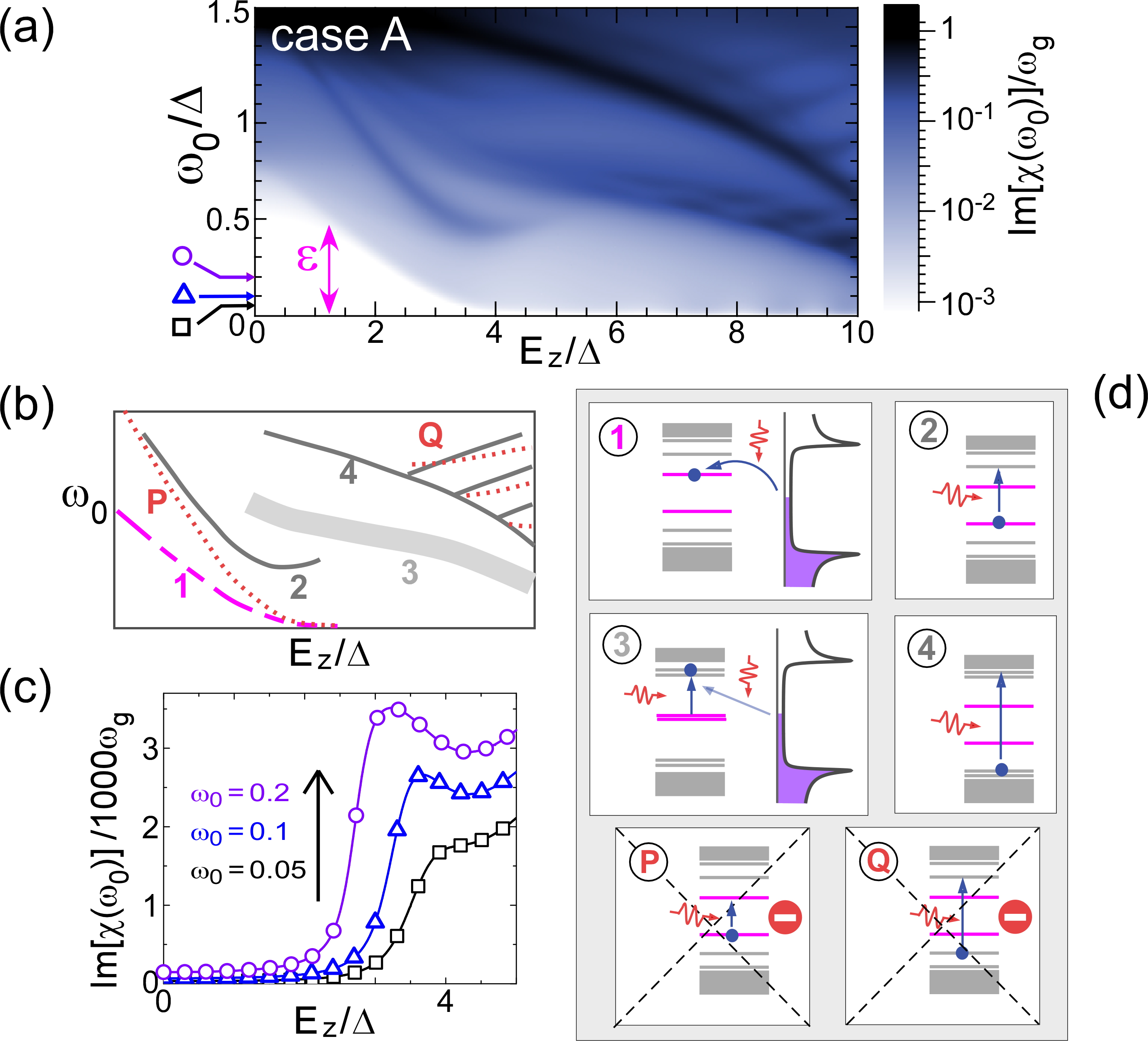
We focus on the dissipative response of the cavity, which should naturally reveal the effects of dissipative reservoirs. We first consider case A where in the topological phase of the nanowire. The map of , shown in Fig.2a with , reveals a wealth of features, sketched in Fig.2b. Feature \tiny{1}⃝ is shown in more details in Fig.2c for constant values of . It consists of a step at , which is the energy distance between one MBS and the Fermi level of the reservoirs. For case A, the effects of the reservoirs on can be disregarded due to the vanishing . Therefore, feature \tiny{1}⃝ can be attributed to photo-induced tunneling between the MBSs and the residual subgap DOS of , as represented in Fig. 2d\tiny{1}⃝. In practice, it is possible to have a well-grounded contact by realizing a direct connection between and the cavity ground plane[48, 37]. In this case, feature \tiny{1}⃝ can exist only if the MBSs are directly coupled to cavity photons, i.e. . In spite of this coupling, no transition occurs at (red dotted line in Fig.2b). The simultaneous presence/absence of a step/resonance at () occurs on a wide range of . We have therefore obtained a signature of the Majorana self-adjoint character[50].
More precisely, these features indicate that we are in presence of a non-degenerate electron/hole conjugated pair, which is the natural precusor of a Majorana pair. It is then important to check from that vanishes with (or shows several zero-energy crossings), as a signature of the spatial isolation of the two MBSs formed out of the non-degenerate electron/hole pair.
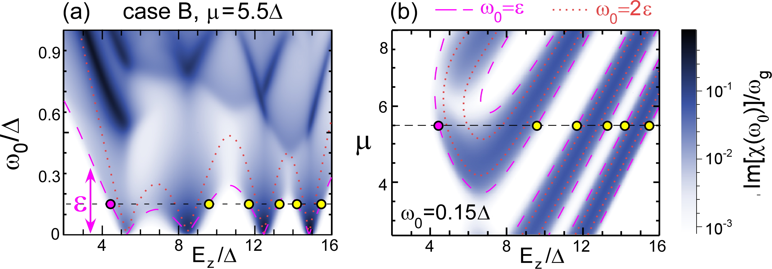
We now demonstrate the robustness of our main results to variations of the nanowire spectrum. Figure 3.a shows the map of in the case of a shorter nanowire (case B). Feature \tiny{1}⃝ persists in this limit, as indicated by the pink circle. Besides, the yellow circles indicate new steps caused again by photo-assisted tunneling from/to the MBSs at . These steps can have a contrast significantly stronger than feature 1. Meanwhile, no resonant feature is visible along the contour indicated by the red dotted line. This extends the possibilities for testing the longitudinal character of the coupling between the Majorana doublet and the cavity. Importantly, feature 1 of case A has an amplitude of . With and a site-cavity coupling , this corresponds to . The pink circle features of case B have an amplitude of which corresponds to . These signals are small but within experimental reach[52, 51], although the residual zero energy DOS in is small, i.e. in case A[B], which leads to the ”hard gap” situation similar to Ref.[53]. Note that in case B, tunneling quasiparticles can be provided by both the and reservoirs, which contribute similarly to the broadening of the low-energy MBSs due to our choice of parameters. We will see later how to distinguish these contributions thanks to a finite bias voltage. Noticeably, an isolated zero energy crossing of two ordinary Andreev bound states could be caused by a trivial spin-degeneracy lifting. However, in this case, the frequency of feature \tiny{2}⃝, which corresponds to an internal nanowire transition inwards/outwards the pair, will not depend on , in contrast with the Majorana case where it strongly depends on due to the topological phase transition[40]. Therefore, our setup is also able to rule out the case of a trivial superconducting wire with time reversal symmetry breaking impurities.
In practice, to measure experimentally signals similar to Figs.2.a and 3a, one must vary . In principle, this is technically possible[54, 55]. However, it is useful to adapt our predictions for standard setups with a fixed . In this case, other parameters must be changed to characterize the nanocircuit[56]. In Fig.3b, we show versus and , for case A. We use which corresponds, with the gap of Al, to the value compatible with present microwave techniques. In these conditions, shows an ensemble of photo-assisted tunneling stripes which reveal the well known oscillations of with and . The correspondence between Figs. 3a and b is given by the pink and yellow circles. The stripes are absent for low values of , where the nanowire makes the transition to its non-topological phase and the MBSs thus disappear. The contours are shown with red dotted lines in Fig.3b. They do not correspond to any remarkable feature in the map of , contrarily to the contours (pink dashed lines). Importantly, in an experiment, the red and pink contours can be determined independently from any theory, by performing a conductance measurement on to get . We conclude that in the case where cannot be varied, a map of and gives an efficient way to characterize the light-matter coupling in our circuit.
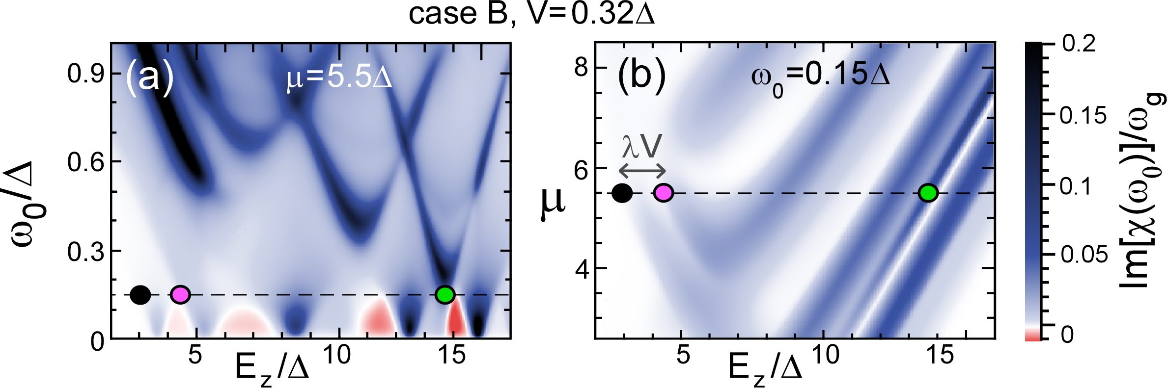
We show below that applying a bias voltage to the hybrid nanocircuit-cavity system[57, 58, 59] enables one to discriminate processes involving the different fermionic reservoirs and to further check that the MBSs are well coupled to cavity photons. Fig.4a shows the map of for case B, with a finite bias voltage applied simultaneously to and . We observe clear differences with the case of Fig.3a. First, a new step marked by the black circle appears, due to tunneling between the MBSs and the reservoirs, at . Meanwhile, the step marked with the pink circle at persists and is now only due to tunneling to . The separation between the black and pink circles, which appears for a finite , is also well visible in the map of (see Fig.4b where ). Second, photon emission revealed by appears for , due to inelastic tunneling between and the upper MBS (red areas in Fig.3a). We conclude that the use of a bias voltage enables a differentiation of the processes involving the and contacts. The persistence of the pink circle feature ensures that cavity photons modulate the potential difference between the MBSs and . Interestingly, for , the upper MBS becomes populated so that internal transitions to upper Andreev levels appear at remarkably low frequencies (see e.g. green circle in Figs.4c and d). This represents another signature of the photon-MBS coupling, although it is not the coupling constant which is involved in this case but rather with and .
In any detection setup, false positive detection events can occur. In our case, a false positive detection of MBSs could happen in the (unlikely) case of a pair of extended non-degenerate Andreev bound states which would have accidentally an energy splitting with the same magnetic field dependence as the non-local pair of localized Majorana modes of Fig. 1b, and a non-conclusive feature 2. To rule out such a situation , one could perform supplementary tests readily accessible in our setup, such as non-local transport measurements using the , and contacts, with, for instance, a varying pair splitting (see for instance Refs.[65, 66, 67]).
To conclude, we have shown how to exploit photo-induced tunneling to check that a pair of MBSs is directly coupled to cavity photons. However, the direct microwave transitions inside the Majorana subspace remains forbidden in a wide range of parameters. This provides a means to check the self-adjoint character of MBSs. Importantly, this protocol is independent from any theory if the conductance of the nanowire is measured simultaneously with the cavity response to determine . Such crossed measurements are routinely achieved with mesoscopic QED devices[58, 37, 61, 60, 62, 63, 49, 64, 59]. Our proposal relies on a nanocircuit geometry widely realized experimentally, and which has reproducibly revealed low energy conductance peaks. Furthermore, nanoconductors with superconducting contacts have been coupled to microwave cavities recently[37, 38, 39]. Therefore, our proposal can be straightforwardly implemented with present experimental means.
Acknowledgements.
Acknowledgements: We thank M.M. Desjardins and L.C. Contamin for useful discussions. This work was financed by the ERC Starting grant CirQys.References
- [1] A. Y. Kitaev, Unpaired Majorana fermions in quantum wires, Phys.Usp. 44, 131 (2001).
- [2] D. A. Ivanov, Non-Abelian Statistics of Half-Quantum Vortices in p-Wave Superconductors, Phys. Rev. Lett. 86, 268 (2001).
- [3] C. Nayak, S. H. Simon, A. Stern, M. Freedman, and S. Das Sarma, Non-Abelian anyons and topological quantum computation, Rev. Mod. Phys. 80, 1083 (2008).
- [4] R. M. Lutchyn, J. D.Sau, and S. Das Sarma, Majorana Fermions and a Topological Phase Transition in Semiconductor-Superconductor Heterostructures, Phys. Rev. Lett. 105, 077001 (2010).
- [5] Y. Oreg, G. Refael, and F. von Oppen, Helical Liquids and Majorana Bound States in Quantum Wires, Phys. Rev. Lett. 105, 177002 (2010).
- [6] V. Mourik, K. Zuo, S. M. Frolov, S. R. Plissard, E. P. A. M. Bakkers, and L. P. Kouwenhoven, Signatures of Majorana Fermions in Hybrid Superconductor-Semiconductor Nanowire Devices, Science 336, 1003 (2012).
- [7] A. Das, Y. Ronen, Y. Most, Y. Oreg, M. Heiblum and H.Shtrikman, Zero-bias peaks and splitting in an Al–InAs nanowire topological superconductor as a signature of Majorana fermions, Nat. Phys. 8, 887 (2012).
- [8] M. T. Deng, C. L. Yu, G. Y. Huang, M. Larsson, P. Caroff, and H. Q. Xu, Anomalous Zero-Bias Conductance Peak in a Nb-InSb Nanowire-Nb Hybrid Device, Nano Letters 12, 6414 (2012).
- [9] H. O. H. Churchill, V. Fatemi, K. Grove-Rasmussen, M. T. Deng, P. Caroff, H. Q. Xu, and C. M. Marcus, Superconductor-nanowire devices from tunneling to the multichannel regime: Zero-bias oscillations and magnetoconductance crossover, Phys. Rev. B 87, 241401 (2013).
- [10] S. M. Albrecht, A. P. Higginbotham, M. Madsen,F. Kuemmeth, T. S. Jespersen, J. Nygård, P. Krogstrup and C. M. Marcus, Exponential protection of zero modes in Majorana islands, Nature 531, 206 (2016).
- [11] T. D. Stanescu, R. M. Lutchyn, and S. Das Sarma, Dimensional crossover in spin-orbit-coupled semiconductor nanowires with induced superconducting pairing, Phys. Rev. B 87, 094518 (2013).
- [12] H. Zhang et al., Ballistic Majorana nanowire devices, arXiv:1603.04069
- [13] J. Liu, A. C. Potter, K. T. Law, and P. A. Lee, Zero-Bias Peaks in the Tunneling Conductance of Spin-Orbit-Coupled Superconducting Wires with and without Majorana End-States, Phys. Rev. Lett. 109, 267002 (2012).
- [14] D. I. Pikulin et al., A zero-voltage conductance peak from weak antilocalization in a Majorana nanowire, New J. Phys. 14, 125011 (2012).
- [15] D. Rainis, L. Trifunovic, J. Klinovaja, and D. Loss, Towards a realistic transport modeling in a superconducting nanowire with Majorana fermions, Phys. Rev. B 87, 024515 (2013).
- [16] D. Roy, N. Bondyopadhaya, S. Tewari, Topologically trivial zero bias conductance peak in semiconductor Majorana wires from boundary effects, Phys. Rev. B 88, 020502(R) (2013).
- [17] E. Zhao, T. Lofwander, J. A. Sauls, Nonequilibrium Superconductivity near Spin Active Interfaces, Phys. Rev. B 70, 134510 (2004)
- [18] A. Cottet and W. Belzig, Conductance and current noise of a superconductor/ferromagnet quantum point contact, Phys. Rev. B 77, 064517 (2008)
- [19] A. Wallraff, D. I. Schuster, A. Blais, L. Frunzio, R.-S.Huang, J. Majer, S. Kumar, S.M. Girvin, and R. J. Schoelkopf, Strong Coupling of a Single Photon to a Superconducting Qubit Using Circuit Quantum Electrodynamics, Nature (London) 431, 162 (2004).
- [20] M. Trif, and Y. Tserkovnyak, Resonantly Tunable Majorana Polariton in a Microwave Cavity, Phys. Rev. Lett. 109, 257002 (2012).
- [21] A. Cottet, T. Kontos, and B. Douçot, Squeezing light with Majorana fermions, Phys. Rev. B 88, 195415 (2013).
- [22] Thomas L. Schmidt, Andreas Nunnenkamp, Christoph Bruder, Microwave-controlled coupling of Majorana bound states, New J. Phys. 15, 025043 (2013).
- [23] O. Dmytruk, M. Trif, and P. Simon, Cavity quantum electrodynamics with mesoscopic topological superconductors, Phys. Rev. B 92, 245432 (2015).
- [24] P. Virtanen, P. Recher, Microwave spectroscopy of Josephson junctions in topological superconductors, Phys. Rev. B 88, 144507 (2013).
- [25] J. I. Väyrynen, G. Rastelli, W. Belzig, L. I. Glazman, Microwave signatures of Majorana states in a topological Josephson junction, Phys. Rev. B 92, 134508 (2015).
- [26] F. Hassler, A. R. Akhmerov and C. W. J. Beenakker, The top-transmon: a hybrid superconducting qubit for parity-protected quantum computation, New J. Phys. 13, 095004 (2011).
- [27] T. Hyart, B. van Heck, I. C. Fulga, M. Burrello, A. R. Akhmerov, and C. W. J. Beenakker, Flux-controlled quantum computation with Majorana fermions, Phys. Rev. B 88, 035121 (2013).
- [28] C. Müller, J. Bourassa, and A. Blais, Detection and Manipulation of Majorana Fermions in Circuit QED, Phys. Rev. B 88, 235401 (2013)
- [29] Z.-Y. Xue, L. B. Shao, Y. Hu, S.-L. Zhu, and Z. D. Wang, Tunable interfaces for realizing universal quantum computation with topological qubits, Phys. Rev. A 88, 024303 (2013).
- [30] D. Pekker, C.-Y. Hou, V. E. Manucharyan, and E. Demler, Phys. Rev. Lett. 111, 107007 (2013).
- [31] E. Ginossar, and E. Grosfeld, Microwave transitions as a signature of coherent parity mixing effects in the Majorana-transmon qubit, Nat. Commun. 5, 4772 (2014).
- [32] C. Ohm and F. Hassler, Microwave readout of Majorana qubits, Phys. Rev. B 91, 085406 (2014).
- [33] K. Yavilberg, E. Ginossar, and E. Grosfeld, Fermion parity measurement and control in Majorana circuit quantum electrodynamics, Phys. Rev. B 92, 075143 (2015).
- [34] K. Yavilberg, E. Ginossar, E. Grosfeld, Fermion parity measurement and control in Majorana circuit quantum electrodynamics, Phys. Rev. B 92, 075143 (2015).
- [35] A. Cottet, T. Kontos, and B. Douçot, Electron-photon coupling in Mesoscopic Quantum Electrodynamics, Phys. Rev. B 91, 205417 (2015).
- [36] C. Janvier, L. Tosi, L. Bretheau, Ç. Ö. Girit, M. Stern, P. Bertet, P. Joyez, D. Vion, D. Esteve, M. F. Goffman, H. Pothier, and C. Urbina, Coherent manipulation of Andreev states in superconducting atomic contacts, Science, 349, 1199 (2015).
- [37] L.E. Bruhat, J.J. Viennot, M.C. Dartiailh, M.M. Desjardins, T. Kontos, A. Cottet, Cavity photons as a probe for charge relaxation resistance and photon emission in a quantum dot coupled to normal and superconducting continua, Phys. Rev. X 6, 021014 (2016).
- [38] T. W. Larsen, K. D. Petersson, F. Kuemmeth, T. S. Jespersen, P. Krogstrup, J. Nygård, and C. M. Marcus, Semiconductor-Nanowire-Based Superconducting Qubit, Phys. Rev. Lett. 115, 127001 (2015).
- [39] G. de Lange, B. van Heck, A. Bruno, D. J. van Woerkom, A. Geresdi, S. R. Plissard, E. P. A. M. Bakkers, A. R. Akhmerov, and L. DiCarlo, Realization of Microwave Quantum Circuits Using Hybrid Superconducting-Semiconducting Nanowire Josephson Elements, Phys. Rev. Lett. 115, 127002 (2015).
- [40] Supplemental Material
- [41] J. Sköldberg, T. Löfwander, V. S. Shumeiko, and M. Fogelström, Spectrum of Andreev Bound States in a Molecule Embedded Inside a Microwave-Excited Superconducting Junction, Phys. Rev. Lett. 101, 087002 (2008).
- [42] E. J. H. Lee, X. Jiang, R. Aguado, G. Katsaros, C. M. Lieber, S. De Franceschi, Zero-bias anomaly in a nanowire quantum dot coupled to superconductors, Phys. Rev. Lett. 109, 186802 (2012).
- [43] For simplicity, we use a which is constant with .
- [44] M. Schiró and K. Le Hur, Tunable Hybrid Quantum Electrodynamics from Nonlinear Electron Transport, Phys. Rev. B 89, 195127 (2014).
- [45] B. K. Agarwalla, M. Kulkarni, S. Mukamel, D. Segal, Tunable photonic cavity coupled to a voltage-biased double quantum dot system: Diagrammatic NEGF approach, arXiv:1604.01811
- [46] B. K. Agarwalla, M. Kulkarni, S. Mukamel, and D. Segal, Giant photon gain in large-scale quantum dot circuit-QED systems, arXiv:1606.01922
- [47] S. K. Lam, A. Pitrou, and S. Seibert Numba: a LLVM-based Python JIT compiler. In Proceedings of the Second Workshop on the LLVM Compiler Infrastructure in HPC (LLVM ’15). ACM, New York, NY, USA (2015).
- [48] In practice, the coupling between the fermionic reservoirs and the cavity photons can be characterized by tuning the nanocircuit in the adiabatic regime where tunneling is much faster than , and using a strong semiclassical microwave excitation, along the lines of Ref.[49].
- [49] M.R. Delbecq, L.E. Bruhat, J.J. Viennot, S. Datta, A. Cottet, T. Kontos, Photon mediated interaction between distant quantum dot circuits, Nature Communications 4, 1400 (2013).
- [50] Decoherence could reduce the visibility of an internal transition between two nanowire states. However, the width of feature \tiny{1}⃝ provides an upper bound for the MBSs broadening . If feature \tiny{1}⃝ is observable and mediated by the coupling constant , it implies that the internal transition at will also be visible in the absence of the self-adjoint property.
- [51] N. Samkharadze, A. Bruno, P. Scarlino, G. Zheng, D. P. DiVincenzo, L. DiCarlo, L. M. K. Vandersypen, High Kinetic Inductance Superconducting Nanowire Resonators for Circuit QED in a Magnetic Field, Phys. Rev. Applied 5, 044004 (2016).
- [52] J. Stehlik, Y.-Y. Liu, C. M. Quintana, C. Eichler, T. R. Hartke, J. R. Petta, Fast charge sensing of a cavity-coupled double quantum dot using a Josephson parametric amplifier, Phys. Rev. Appl. 4, 014018 (2015).
- [53] W. Chang, S. M. Albrecht, T. S. Jespersen, F. Kuemmeth, P. Krogstrup, J. Nygård, C. M. Marcus, Hard gap in epitaxial semiconductor-superconductor nanowires, Nature Nanotechnology 10, 232 (2015).
- [54] A. Palacios-Laloy, F. Nguyen, F. Mallet, P. Bertet , D. Vion, D. Esteve, Tunable Resonators for Quantum Circuits, J. Low Temp. Phys. 151, 1034 (2008).
- [55] M. Sandberg, C. M. Wilson, F. Persson, T. Bauch, G. Johansson, V. Shumeiko, T. Duty and P. Delsing, Tuning the field in a microwave resonator faster than the photon lifetime, Appl. Phys. Lett. 92, 203501 (2008).
- [56] J. J. Viennot, M. C. Dartiailh, A. Cottet, and T. Kontos, Coherent coupling of a single spin to microwave cavity photons, Science 349, 408 (2015).
- [57] Y.-Y. Liu, J. Stehlik, C. Eichler, M. J. Gullans, J. M. Taylor, and J. R. Petta, Semiconductor double quantum dot micromaser, Science 347, 285 (2015).
- [58] J. J. Viennot, M. R. Delbecq, M. C. Dartiailh, A. Cottet, and T. Kontos, Out-of-equilibrium charge dynamics in a hybrid circuit quantum electrodynamics architecture, Phys. Rev. B 89, 165404 (2014).
- [59] A. Stockklauser, V. F. Maisi, J. Basset, K. Cujia, C. Reichl, W. Wegscheider, T. Ihn, A. Wallraff, and K. Ensslin, Microwave Emission from Hybridized States in a Semiconductor Charge Qubit, Phys.Rev. Lett. 115, 046802 (2015).
- [60] M.R. Delbecq, V. Schmitt, F.D. Parmentier, N. Roch, J.J. Viennot, G. Fève, B. Huard, C. Mora, A. Cottet, and T. Kontos, Coupling a Quantum Dot, Fermionic Leads, and a Microwave Cavity on a Chip, Phys. Rev. Lett. 107, 256804 (2011).
- [61] T. Frey, P. J. Leek, M. Beck, A. Blais, T. Ihn, K. Ensslin, and A. Wallraff, Dipole Coupling of a Double Quantum Dot to a Microwave Resonator, Phys. Rev. Lett. 108, 046807 (2012).
- [62] K. D. Petersson, C. G. Smith, D. Anderson, P. Atkinson, G. A. C. Jones, D. A. Ritchie, Charge and spin state readout of a double quantum dot coupled to a resonator, Nano Lett. 10, 2789-2793 (2010).
- [63] K. D. Petersson, L. W. McFaul, M. D. Schroer, M. Jung, J. M. Taylor, A. A. Houck, J. R. Petta, Circuit Quantum Electrodynamics with a Spin Qubit, Nature 490, 380 (2012).
- [64] Y.-Y. Liu, K. D. Petersson, J. Stehlik, J. M. Taylor, J. R. Petta, Photon Emission from a Cavity-Coupled Double Quantum Dot, Phys. Rev. Lett. 113, 036801 (2014).
- [65] C. J. Bolech and E. Demler, Observing Majorana bound States in p-Wave Superconductors Using Noise Measurements in Tunneling Experiments, Phys. Rev. Lett. 98, 237002 (2007)
- [66] J. Nilsson, A. R. Akhmerov, and C. W. J. Beenakker, Splitting of a Cooper Pair by a Pair of Majorana Bound States, Phys. Rev. Lett. 101, 120403 (2008).
- [67] J. Liu, F.-C. Zhang, and K. T. Law, Majorana Fermion Induced Non-local Current Correlations in Spin-orbit Coupled Superconducting Wires, Phys. Rev. B 88, 064509 (2013)