Scattering mechanisms of highest-mobility InAs/AlxGa1-xSb quantum wells
Abstract
We study molecular beam epitaxially grown, undoped AlxGa1-xSb/InAs/AlSb quantum wells with different buffer and barrier designs and varying quantum well width. The highest mobilities were achieved with Al0.33Ga0.67Sb buffers and lower barriers and a quantum well width of 24 nm. These quasi-single-interface InAs/AlSb quantum well devices reached a gate-tuned mobility of 2.4 cm2/Vs at a density of 1 cm-2 and 1.3 K. In Hall bar devices boundary scattering is found to strongly influence the mobility determination in this mobility regime. Ionized background impurity scattering at low electron densities, device boundary scattering at intermediate electron densities, and intersubband scattering at high electron densities were identified as the most likely dominant scattering processes. Ringlike structures in the Landau fan can be explained using a single-particle model of crossing Landau levels.
pacs
73.21.FgI Introduction
Heterostructures containing InAs have been studied due to their potential applications in high-speed, low power-electronics, such as in heterostructure field effect transistors (HFETs)[1] and THz imaging and sensing [2]. The large band offset between InAs and the AlSb barriers results in excellent carrier confinement and enhanced radiation tolerance[3]. Its narrow band gap and strong spin-orbit coupling makes the system ideal for spintronic devices research [4, 5, 6]. In recent years research on InAs quantum wells has gained significance due to their similarity to InAs/GaSb composite quantum wells for topological insulators [7] and due to new prospects for realizing a topological superconducting phase supporting Majorana fermions when combined with -wave superconductors [8, 9, 10].
The carrier mobility of InAs quantum wells[11, 12, 13, 14] has for a long time been confined to regions below cm2/Vs, whereas GaAs/AlGaAs heterostructures can reach mobility values above cm2/Vs[15, 16, 17, 18] despite their higher effective mass. This implies that there is ample room for improving the growth techniques and structure designs of InAs quantum wells.
The recent availability of high-quality, almost lattice-matched GaSb substrates has led to a steep increase of growth quality and the subsequent carrier mobilities[13]. Shojaei et al.[14] recently showed that the mobilities of InAs quantum wells with Al0.8Ga0.2Sb barriers and well widths of up to 15 nm scaled in accordance with Coulombic scattering from charged defects at low electron density. For high densities the gate-tuned mobility of those structures was limited to 0.75 cm2/Vs by interface roughness scattering and alloy disorder scattering. In this work we show that by further optimizing structural design parameters, the mobility can be drastically increased. The highest low-temperature mobility achieved was 2.402 cm2/Vs at a carrier density of 10.19 cm-2, which is more than double the mobility of any other published InAs quantum well. We present temperature and density dependent magnetotransport measurements on these samples to identify the remaining limiting scattering mechanisms in this mobility regime.
II Samples and ungated measurements
All studied samples were grown in a modified Veeco Gen II molecular beam epitaxy (MBE) system. The protective oxide was entirely thermally desorbed from the GaSb substrates inside the MBE at 540 ∘C. All temperatures were measured using a BandIT system with blackbody radiation fitting and the growth rates were calibrated using reflection high-energy electron diffraction (RHEED).

After the oxide was completely desorbed and typical GaSb RHEED patterns were clearly visible, the growth on all samples was initiated with a 600 nm thick GaSb layer grown at 530 ∘C. This layer was followed by a 10 period Al0.33Ga0.67Sb/GaSb superlattice. Towards the end of the ensuing 200 nm lower barrier, the substrate temperature was lowered to 425 ∘C and the InAs quantum well was grown using the shutter sequence proposed by Tuttle et al.[19]. Before and after the InAs layer, when the group V element changes from Sb to As and back again, we introduced a 30 second growth pause to reduce the group V element intermixing and the consequential alloy scattering in the samples. During the InAs layer growth the temperature was increased again towards 480 ∘C and the following 20 nm upper barrier and 5 nm GaSb cap layer were again grown at 530 ∘C.

We first grew a series of samples with a quantum well width of 15 nm, AlSb upper barrier, and varying lower barrier composition listed in Table 1. The first three samples demonstrate the reproducibility of the achieved electron densities and mobilities. Decreasing the aluminium content in the AlxGa1-xSb buffer and barriers reduces the lattice mismatch to the GaSb substrate and to the InAs in the quantum well. But this also causes the valence band energy of the barriers to rise relative to the conduction band energy of the quantum well. Reducing the aluminium fraction roughly below triggers a transition from a semiconductor to a semimetal, where the electrons can transfer from the AlxGa1-xSb valence band to the InAs conduction band, inducing holes in the AlxGa1-xSb layer[20]. This is illustrated in a self-consistent 88 kp simulation[21] in Fig. 1 and the consequences emerge in the samples D and E, where the mobilities drop with lower aluminium content. Hence, we chose an aluminium fraction of for the buffer and the lower barriers.
Also samples with Al0.33Ga0.67Sb upper barriers were tested, shown in Table 2. The intrinsic electron density with this upper barrier tends to decrease. We therefore reduced the upper barrier width to compensate that effect and keep the density in the same region as the other samples. Despite the slightly higher carrier concentrations, these wells yield lower mobilities than their counterparts with equal well width. We attribute this to the lower confinement energy resulting in a larger fraction of the electron wave function being inside the upper barrier and thus increasing alloy scattering, as illustrated in an 88 kp simulation shown in Fig. 2. The closer surface is also likely to increase remote impurity scattering. These effects seem to outweigh the more similar lattice constants of the quantum well and the upper barrier, which is apparently of less significance than the closer matched lattice constants between the quantum well and the lower barrier. This result is also noteworthy in the context of recent experiments on high-mobility GaAs quantum wells with either AlGaAs or AlAs barriers[22]. There, a mobility reduction was observed for GaAs/AlAs interfaces.
| Sample | lower barrier | [cm-2] | [cm2/Vs] |
|---|---|---|---|
| A | Al0.33Ga0.67Sb | 7.536 | 8.613 |
| B | Al0.33Ga0.67Sb | 7.724 | 8.207 |
| C | Al0.33Ga0.67Sb | 7.458 | 8.229 |
| D | Al0.15Ga0.85Sb | 7.747 | 7.088 |
| E | GaSb | 9.609 | 1.523 |
| Sample | [nm] | [nm] | [cm-2] | [cm2/Vs] |
|---|---|---|---|---|
| F | 12 | 10 | 8.200 | 2.432 |
| G | 21 | 10 | 8.821 | 7.282 |
| H | 15 | 50 | 3.878 | 3.724 |
The samples with the lower Al0.33Ga0.67Sb barrier and 20 nm wide upper AlSb barrier yield the highest intrinsic mobilities and densities, the highest mobility being 0.861 cm2/Vs at a carrier density of 7.54 cm-2 measured at 1.3 K. We produced a series of similar samples only varying in quantum well width shown in Table 3. As expected[23, 24, 25], the mobility decreases for narrowing well width due to increased interface roughness scattering. For wells wider than 15 nm, the mobility keeps increasing with an almost constant carrier density up to 1.847 cm2/Vs at a density of 7.99 cm-2 for the widest sample (Fig. 3).
It was previously assumed that in InAs quantum wells (QWs) wider than 15 nm, the mobility starts to decrease again because the critical thickness of the InAs layer is exceeded and misfit dislocations start to nucleate[24], or due to the earlier onset of intersubband scattering[26]. The intrinsic density of our samples is not high enough for electrons to populate the second subband even in the widest grown samples. When the lattice mismatch between the substrate and the crystal epitaxially grown upon it is reduced, less strain energy is accumulated and therefore the critical layer thickness at which the structure relaxes to the substrate lattice constant is extended[27]. Together with the improved growth on GaSb substrates[28] it seems possible to grow wider quantum wells and further reduce the mobility-limiting interface roughness scattering.
| Sample | [nm] | [cm-2] | [cm2/Vs] |
|---|---|---|---|
| I | 8 | 6.311 | 0.871 |
| J | 12 | 7.342 | 4.083 |
| A | 15 | 7.536 | 8.613 |
| K | 18 | 8.151 | 13.44 |
| L | 21 | 7.208 | 17.58 |
| M | 24 | 7.994 | 18.47 |

The increase of mobility with well width flattens from 21 nm to 24 nm. For a further increased well width the improvements are expected to be minimal, because all wider wells would effectively be InAs/AlSb single-interface quantum wells with a triangular well for the first electron level, as shown in the simulation in Fig. 1 b).
III Boundary scattering in narrow Hall bars
Hall bars were fabricated out of the two widest quantum well samples L and M using dry or wet etching as in Pal et al.[29]. Those were passivated with a 200 nm thick Si3N4 dielectric and covered with a Ti/Au top gate[30].
In a magnetic field, electron trajectories are deflected by the Lorentz force. When the resulting curvature is sufficient and the elastic mean-free path of the electrons becomes comparable to or larger than the effective electronic width of a long Hall bar (), the scattering with the edge becomes more relevant than scattering with potential fluctuations in the bulk of the sample. This boundary scattering appears in the measurements as an enhanced longitudinal resistivity at small magnetic fields[31, 32, 33], peaking at according to
| (1) |
Here, is the cyclotron radius and is the Fermi wave vector.
Measurements of the 10 m wide Hall bars show peaks at finite in both processed wafers [Fig. 4(a)], whose position scales with according to Eq. (1). For the 25 m wide Hall bars the peaks are significantly smaller compared to the background resistivity and are even more reduced for the 400 m wide Hall bars [Fig. 4(b)]. In the ungated square samples the peaks have not been detected. Therefore we suspect the zero-field peaks to be an effect of the device size and most likely the boundary scattering introduced before.


The enhanced zero-field longitudinal resistivity affects the calculated mobility versus density graph in a nonlinear way due to the density and mobility dependencies of the resistivity peaks (Fig. 5). For smaller Hall bars with presumably stronger boundary scattering the mobility curve starts to flatten at lower densities than in wider Hall bar devices. As the zero-field peak did not vanish completely in the 400 m wide Hall bar it is likely that the flattening of the corresponding mobility curve at higher electron density is caused by residual boundary scattering also in this device.
The mean-free path at the highest mobility was m for sample L and m for sample M, calculated with[34] . This was measured using the zero-field longitudinal resistivities from the widest Hall bar devices. Although these values are one order of magnitude shorter than the Hall bar width, still some residual boundary scattering seems to influence the measurements and enhances the low-field longitudinal resistance and thereby lowers the measured mobility. In the following analysis we used the measurements with the 400 m wide and 650 m long Hall bars where the zero-field peaks are the smallest.
The influence of boundary scattering in InAs devices has previously only been relevant for extremely narrow Hall bar devices[29]. With increasing sample quality this additional scattering source also manifests itself by limiting the electron mobility in standard Hall bar sizes and has to be taken into account when fabricating devices.
IV Intrinsic scattering mechanisms
IV.1 Electron mobility

The carrier mobility in high-mobility electronic systems typically shows a power law dependence on the carrier density . The exponent of scaling, called the parameter, is a useful tool to characterize the dominant scattering mechanisms in those systems[35].

The dependence of the mobility on electron density for sample L is shown in Fig. 5. A fit to the logarithm of the low-density mobility reveals an parameter of roughly 0.73 before the curve flattens. However, the accuracy of this value is limited by the small fitting range in density. This is fairly close to the theoretically predicted parameter for two-dimensional systems with 3D-distributed 3D Coulomb disorder in the strong-screening limit[35] of 0.5. It also aligns nicely with the exponents of 0.7 to 0.8 reported for high-mobility GaAs/AlGaAs heterostructures[36, 37, 38, 39]. In these structures such an exponent is commonly associated with dominant scattering by ionized background impurities.
At higher densities the curve flattens and reaches a maximum value of 2.402 cm2/Vs at a carrier density of 10.19 cm-2. This could be a sign of interface roughness scattering becoming dominant or the influence of the residual boundary scattering studied in the previous chapter. Because the boundary scattering leads to an additional longitudinal resistivity only for small magnetic fields and the remaining longitudinal resistivity is constant until the onset of Shubnikov de Haas oscillations (Fig. 6), it can be artificially removed in the data by calculating the mobilities using the longitudinal resistivity values at small magnetic fields beyond the onset of the peaks. When this is done using the longitudinal resistivity at a magnetic field of 0.11 T, the mobility curve follows an almost straight line until reaching a maximum value of 3.219 cm2/Vs and then dropping abruptly (Fig. 7). The parameter for the low to intermediate density regime in this case is 0.83, still consistent with dominant scattering by ionized background impurities. From the absence of a flattening in this case we infer that the boundary scattering is the limiting factor in this density regime in our devices.
At an electron density of approximately 11 cm-2 for sample L and 9 cm-2 for sample M a sudden drop in mobility reveals the onset of intersubband scattering, where the electrons start to fill the second subband. These density values correspond to subband separation energies of eV and eV using[40] , consistent with our 88 kp simulations. The effective masses used in this calculations were and for the corresponding densities of samples L and M, determined as shown in the next chapter.
IV.2 Quantum scattering time
The quantum scattering time is related to the broadening of the Landau levels and characterizes the momentum relaxation of a quasiparticle in two-dimensional transport. Together with the transport scattering time it can reveal the long-range or short-range nature of the existing scattering potentials. We measured the low-field Shubnikov–de Haas oscillations of the two highest-mobility samples L and M at different gate voltages to determine the quantum scattering time with varying electron density.
To correctly calculate the quantum scattering time, one has to take the density-dependent effective mass of InAs into account. The Shubnikov-de Haas oscillations in both samples were measured at different gate voltages over a temperature range from 1.3 K to 20 K. The effective mass was calculated via the temperature-dependence of the oscillations using the method from Braña et al[40]. The envelope of the oscillations in longitudinal resistivity is given by [34, 41]
| (2) |
where , is the cyclotron frequency, and is the nonoscillatory background resistivity. The amplitude of the oscillations scales with temperature as
| (3) |
Using , we can define
| (4) |
and it follows that
| (5) |
When is calculated from the measured amplitudes and plotted against the temperature , the effective mass is incorporated in the slope as well as in itself. This equation has to be solved repeatedly until both effective masses match.
We calculated the effective masses from all peaks in the magnetic field range where zero-field spin-splitting beatings do not occur and before the onset of spin-orbit coupling induced spin splitting, which is roughly between 0.8 T and 1.8 T depending on sample and electron density. The calculated values did not show any significant magnetic field dependence in the respective ranges.
The average of for all peaks at the corresponding electron densities is shown in Fig. 8. The dashed lines are the effective masses calculated from the bulk effective mass using the formula derived by Ando[42],
| (6) |
where is the Fermi energy, the band gap energy, the bulk effective mass, and is the enhancement of the effective mass in a quantum well over the bulk effective mass. The kinetic energy can be approximated for a triangular well with , where is the energy of the first subband calculated using 88 kp simulations. The Fermi energy is given by . The bulk effective mass for the theoretical calculation fitting the measurement best was , which lies comfortably in the range of reported values[43] for InAs.

The measured masses match the model very well. Besides the higher precision of the measurements of sample L, there was no clear difference between the two well widths. This is in accordance with the theoretical calculations, in which the masses of the two quantum wells with different width deviate slightly from each other only at low densities.
These masses were now used in the calculation of the quantum scattering time . By plotting
| (7) |
versus at constant temperature, one can calculate from the slope of the resulting straight lines[34]. Only the results of valid fits are shown[44], where the plots are straight lines and the intercepts at are close to 1.
The measured quantum scattering time for both samples at 1.3 K is presented in Fig. 9 a). It fluctuates for both samples roughly around s. For sample M is constant over the whole density range. For sample L it exhibits a slight apparent decrease with increasing carrier density. Such a decrease can be caused by interface roughness scattering[45]. We deem this unlikely, because the apparent decrease in our sample occurs over the whole gate range instead of only at high densities where interface roughness scattering is supposed to dominate.
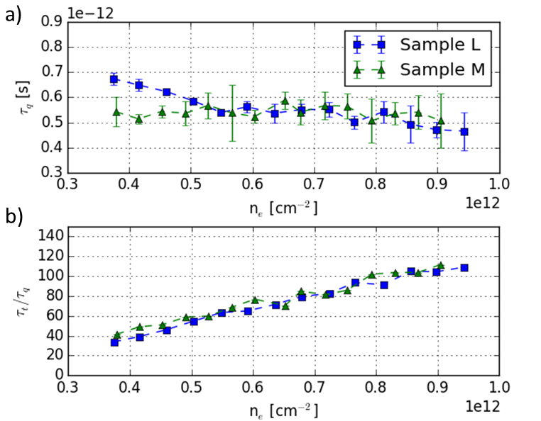
The Dingle ratio, defined as /, where is the transport lifetime, can be taken as an indication of the nature of the the scattering potential[46, 47]. is weighted heavily towards large-angle scattering events and is affected by scattering events of all angles. For short-range isotropic scattering both lifetimes should be almost equally affected and a ratio close to 1 is expected. For scattering by long-range Coulomb interactions is only weakly affected and the ratio / is considerably larger.
Figure 9(b) shows the measured Dingle ratio for both samples. At low densities both samples have a Dingle ratio of roughly 40, which is comparable to reported Dingle ratios in high-mobility GaAs and in SiGe quantum wells[48, 44, 49]. For higher densities the Dingle ratios of both samples increase in unison, indicating even smoother scattering potentials. We explain this by the extremely high electron density shielding remote scatterers and thus smoothing out their scattering potential. The slight decrease of in sample L has no significant influence on this ratio as the result of both samples is very similar.
As a result of this analysis we suspect the dominant scattering in this density regime to stem from long-range Coulomb interactions with ionized impurities predominantly remote to the well. The boundary scattering from the previous chapter does not appear in this analysis because is measured at higher magnetic fields where the zero-field peak in longitudinal resistance is irrelevant.
V Landau fan
In the high electron density regime, where two subbands are occupied, both samples show peculiar, ringlike features in their Landau fans (Fig. 10). Similar features were also observed in GaAs/AlGaAs heterostructures[50, 51, 52, 53, 54] with two occupied subbands or in a tilted magnetic field. Despite the usually higher single subband mobilities of the GaAs/AlGaAs system, these samples only reached a mobility of about 0.6 cm2/Vs or less in the two-subband regime due to strong intersubband scattering and heavy doping. The studied InAs samples exhibit a comparable mobility in their second subband regime and the ringlike features are clearly visible at measurement temperatures of 1.3 K.

These peculiar structures can be reasonably reproduced using a single-particle model introduced by Ellenberger et al. for GaAs/AlGaAs heterostructures[52]. The evolution of the Landau level energy in a magnetic field is given by
| (8) | |||||
| (9) |
for the respective subbands 1 and 2 with the Landau-level quantum number and the two spin directions . The crucial step in this model is the highly nonlinear mapping from the energy–magnetic field plane to the density–magnetic field plane. This is achieved by assuming Gaussian-broadened Landau levels which can be maximally occupied by electrons per area. After this mapping, the ringlike structures appear in the simulation.
The g-factor of for the simulation was determined from the crossing points in the Landau fan as in Ellenberger et al. The effective mass of the first electron subband at this density was determined using the theoretical curve calculated along the measurements presented earlier (Fig. 8). The effective mass of the second subband in this density range was estimated using 88 kp simulations as . The measured quantum scattering time s yields a level broadening of 600 eV, using .
The energy separation of the first and second electron subband varies with density because the top gate influences the shape of the quantum well. This was implemented using a linear fit of the energy separations at various densities determined from crossing points in the Landau fan. The obtained energy separations are in close agreement to self-consistent 88 kp simulations and with the values calculated from the onset of the second subband in the mobility curve.
Figure 11 shows the simulated crossing of the three spin-split Landau levels from the first subband with the Landau level from the second subband and the corresponding region in the measurement. This single-particle picture matches the experiment remarkably well with input parameters only from measurement and 88 kp simulations.

VI Conclusion
We have grown a range of undoped InAs quantum wells with different buffer and barrier structures and quantum well widths using molecular beam epitaxy. We found that lower AlxGa1-xSb buffers and barriers with yield the highest intrinsic electron mobilities. Extending the quantum well width beyond the widely used 15 nm towards 24 nm yields another dramatic improvement in mobility. 88 kp simulations show that these widest structures are quasi-single-interface InAs/AlSb quantum wells. The highest ungated mobility achieved was 1.847 cm2/Vs at a density of 7.99 cm-2.
By manufacturing Hall bars with top gates we were able to tune the electron density and increase the mobility to a maximum of 2.402 cm2/Vs at a density of 10.19 cm-2. We found the size of these Hall bars to heavily influence the measured mobilities. Since the elastic mean-free path of the electrons at mobilities this high easily reaches the width of standard Hall bars, scattering at the device boundaries enhances the low magnetic field longitudinal resistivity considerably.
The density-dependent effective mass of the highest-mobility samples was measured and it agrees with theoretical calculations. The measured quantum scattering time and its relation to the transport scattering time of these samples indicate that their most important sources of scattering for a nonzero magnetic field and before the population of the second subband are likely to be ionized impurities predominantly remote to the well. This is supported by the scaling exponent relating the carrier mobility to the carrier density. For lower densities it has a value of consistent with dominant scattering by background impurities as in high-mobility GaAs/AlGaAs structures. For higher densities scattering at the device boundaries becomes the limiting factor and at even higher densities the onset of intersubband scattering causes a sudden drop in mobility.
We also encountered ringlike features in the Landau fans of our two highest-mobility samples. These features arise from the crossing of spin-split Landau levels of two different subbands and were modeled using a single-particle picture.
Acknowledgements.
The authors acknowledge financial support by the Swiss National Science Foundation (SNF) through the NCCR ’QSIT – Quantum Science and Technology’ (National Centre of Competence in Research).References
- [1] N.-T. Yeh, P.-C. Chiu, J.-I. Chyi, F. Ren, and S. J. Pearton, J. Mater. Chem. C 1, 4616 (2013).
- [2] M. Brandstetter, M. A. Kainz, T. Zederbauer, M. Krall, S. Schönhuber, H. Detz, W. Schrenk, A. M. Andrews, G. Strasser, and K. Unterrainer, Applied Physics Letters 108, 011109 (2016), http://dx.doi.org/10.1063/1.4939551.
- [3] B. D. Weaver, J. B. Boos, N. A. Papanicolaou, B. R. Bennett, D. Park, and R. Bass, Applied Physics Letters 87, 173501 (2005), http://dx.doi.org/10.1063/1.2115071.
- [4] S. Datta and B. Das, Applied Physics Letters 56, 665 (1990).
- [5] I. Zutic, J. Fabian, and S. Das Sarma, Rev. Mod. Phys. 76, 323 (2004).
- [6] D. D. Awschalom and M. E. Flatte, Nat Phys 3, 153 (2007).
- [7] C. Liu, T. L. Hughes, X.-L. Qi, K. Wang, and S.-C. Zhang, Phys. Rev. Lett. 100, 236601 (2008).
- [8] J. D. Sau, R. M. Lutchyn, S. Tewari, and S. Das Sarma, Phys. Rev. Lett. 104, 040502 (2010).
- [9] J. Alicea, Phys. Rev. B 81, 125318 (2010).
- [10] R. M. Lutchyn, J. D. Sau, and S. Das Sarma, Phys. Rev. Lett. 105, 077001 (2010).
- [11] C. Nguyen, Ph.D. thesis, University of California at Santa Barbara (1993).
- [12] M. Thomas, H.-R. Blank, K. Wong, and H. Kroemer, Journal of Crystal Growth 175-176, 894 (1997).
- [13] B. Shojaei, A. McFadden, J. Shabani, B. D. Schultz, and C. J. Palmstrøm, Applied Physics Letters 106, 222101 (2015), http://dx.doi.org/10.1063/1.4921970.
- [14] B. Shojaei, A. C. C. Drachmann, M. Pendharkar, D. J. Pennachio, M. P. Echlin, P. G. Callahan, S. Kraemer, T. M. Pollock, C. M. Marcus, and C. J. Palmstrom, Phys. Rev. B 94, 245306 (2016).
- [15] S. Riedi, C. Reichl, M. Berl, L. Alt, A. Maier, and W. Wegscheider, Journal of Crystal Growth 455, 37 (2016).
- [16] G. C. Gardner, S. Fallahi, J. D. Watson, and M. J. Manfra, Journal of Crystal Growth 441, 71 (2016).
- [17] D. G. Schlom and L. N. Pfeiffer, Nat Mater 9, 881 (2010).
- [18] V. Umansky, M. Heiblum, Y. Levinson, J. Smet, J. Nübler, and M. Dolev, Journal of Crystal Growth 311, 1658 (2009).
- [19] G. Tuttle, H. Kroemer, and J. H. English, Journal of Applied Physics 67, 3032 (1990).
- [20] I. Lo, W. C. Mitchel, and J.-P. Cheng, Phys. Rev. B 50, 5316 (1994).
- [21] Simulations were carried out using the nextnano software (www.nextnano.com).
- [22] D. Kamburov, K. W. Baldwin, K. W. West, M. Shayegan, and L. N. Pfeiffer, Applied Physics Letters 109, 232105 (2016), http://aip.scitation.org/doi/pdf/10.1063/1.4971824 .
- [23] H. Sakaki, T. Noda, K. Hirakawa, M. Tanaka, and T. Matsusue, Applied Physics Letters 51, 1934 (1987).
- [24] C. R. Bolognesi, H. Kroemer, and J. H. English, J. Vac. Sci. Technol. B 10, 877 (1992a).
- [25] C. R. Bolognesi, H. Kroemer, and J. H. English, Applied Physics Letters 61, 213 (1992b).
- [26] H. Kroemer, Physica E: Low-dimensional Systems and Nanostructures 20, 196 (2004), proceedings of the 11th International Conference on Narrow Gap Semiconductors.
- [27] U. W. Pohl, Epitaxy of Semiconductors (Springer-Verlag, Berlin Heidelberg, 2013).
- [28] B. R. Bennett, Applied Physics Letters 73, 3736 (1998).
- [29] A. N. Pal, S. Müller, T. Ihn, K. Ensslin, T. Tschirky, C. Charpentier, and W. Wegscheider, AIP Advances 5, 077106 (2015), http://dx.doi.org/10.1063/1.4926385.
- [30] S. Mueller, A. N. Pal, M. Karalic, T. Tschirky, C. Charpentier, W. Wegscheider, K. Ensslin, and T. Ihn, Phys. Rev. B 92, 081303 (2015).
- [31] E. Ditlefsen and J. Lothe, Philosophical Magazine 14, 759 (1966), http://dx.doi.org/10.1080/14786436608211970 .
- [32] C. W. J. Beenakker and H. van Houten, Phys. Rev. Lett. 63, 1857 (1989).
- [33] T. J. Thornton, M. L. Roukes, A. Scherer, and B. P. Van de Gaag, Phys. Rev. Lett. 63, 2128 (1989).
- [34] T. Ihn, Semiconductor Nanostructures (Oxford University Press New York, 2010).
- [35] S. Das Sarma and E. H. Hwang, Phys. Rev. B 88, 035439 (2013).
- [36] M. Shayegan, V. J. Goldman, C. Jiang, T. Sajoto, and M. Santos, Applied Physics Letters 52, 1086 (1988), http://aip.scitation.org/doi/pdf/10.1063/1.99219 .
- [37] L. Pfeiffer, K. W. West, H. L. Stormer, and K. W. Baldwin, Applied Physics Letters 55, 1888 (1989).
- [38] A. Gold, Applied Physics Letters 54, 2100 (1989).
- [39] V. Umansky, R. de Picciotto, and M. Heiblum, Applied Physics Letters 71, 683 (1997).
- [40] A. F. Braña, C. Diaz-Paniagua, F. Batallan, J. A. Garrido, E. Muñoz, and F. Omnes, Journal of Applied Physics 88, 932 (2000).
- [41] P. T. Coleridge, R. Stoner, and R. Fletcher, Phys. Rev. B 39, 1120 (1989).
- [42] T. Ando, Journal of the Physical Society of Japan 51, 3893 (1982), http://dx.doi.org/10.1143/JPSJ.51.3893 .
- [43] I. Vurgaftman, J. R. Meyer, and L. R. Ram-Mohan, Journal of Applied Physics 89, 5815 (2001).
- [44] P. T. Coleridge, Phys. Rev. B 44, 3793 (1991).
- [45] I. Lo, W. C. Mitchel, M. O. Manasreh, C. E. Stutz, and K. R. Evans, Applied Physics Letters 60, 751 (1992).
- [46] A. Gold, Phys. Rev. B 38, 10798 (1988).
- [47] S. Peters, L. Tiemann, C. Reichl, and W. Wegscheider, Phys. Rev. B 94, 045304 (2016).
- [48] F. Fang, T. Smith, and S. Wright, Surface Science 196, 310 (1988).
- [49] K. Ismail, M. Arafa, K. L. Saenger, J. O. Chu, and B. S. Meyerson, Applied Physics Letters 66, 1077 (1995).
- [50] K. Muraki, T. Saku, and Y. Hirayama, Phys. Rev. Lett. 87, 196801 (2001).
- [51] X. C. Zhang, D. R. Faulhaber, and H. W. Jiang, Phys. Rev. Lett. 95, 216801 (2005).
- [52] C. Ellenberger, B. Simovič, R. Leturcq, T. Ihn, S. E. Ulloa, K. Ensslin, D. C. Driscoll, and A. C. Gossard, Phys. Rev. B 74, 195313 (2006).
- [53] X. C. Zhang, I. Martin, and H. W. Jiang, Phys. Rev. B 74, 073301 (2006).
- [54] G. M. Gusev, C. A. Duarte, A. A. Quivy, T. E. Lamas, and J. C. Portal, AIP Conference Proceedings 893, 627 (2007).