Uniform Benchmarking of Low Voltage Van Der Waals FETs
Abstract
Monolayer MoS2, MoSe2, MoTe2, WS2, WSe2, and black phosphorous field effect transistors (FETs) operating in the low-voltage (LV) regime (0.3V) with geometries from the 2019 and 2028 nodes of the 2013 International Technology Roadmap for Semiconductors (ITRS) are benchmarked along with an ultra-thin-body Si FET. Current can increase or decrease with scaling, and the trend is strongly correlated with the effective mass. For LV operation at the 2028 node, an effective mass of , corresponding to that of WSe2, gives the maximum drive current. The short 6 nm gate length combined with LV operation is forgiving in its requirements for material quality and contact resistances. In this LV regime, device and circuit performance are competitive using currently measured values for mobilities and contact resistances for the monolayer two-dimensional materials.
Index Terms:
FET, van der Waals materials, 2D materials, transition metal dichalcogenide, black phosphorous, UTB Si, benchmarkingI Introduction
There is significant interest in understanding how two-dimensional (2D) semiconductors compare with traditional semiconductors for use as the channel material in ultra-scaled field effect transistors (FETs). The FET also serves as a baseline device for determining targets for material parameters. For example, given a set of FET performance specifications such as drive current, switching energy, switching delay, etc., one can then ask, “What material parameters, such as, for example, mobility, effective mass, bandgap, or contact resistance, are sufficient to achieve these device performance metrics?” One can also enquire, “What material parameters optimize the device performance?” Thus, benchmarking of a baseline device provides top-down targets for materials benchmarking [1].
Promising 2D semiconductors include the transition metal dichalcogenides (TMDs) with the chemical form MX2 where M = Mo or W and X = S, Se or Te [2, 3, 4, 5, 6, 7, 8, 9], and bandgaps in the range of 1–2 eV [6, 3]. A more recent addition to the van der Waals (vdW) class of materials for field effect transistor (FET) applications is black phosphorus (BP) [10, 11, 12]. BP’s large field effect mobility and highly anisotropic bandstructure make it a promising material for FET applications [13, 10, 14, 11, 15, 16].
A number of articles in the literature have theoretically predicted the performance of these alternate materials for future device applications. While the majority of the performance predictions are for MoS2 FETs [17, 18, 19, 20, 21, 22, 23, 24] and BP [14], some of them focus on device comparisons within the TMD group for conventional FETs [25, 26, 27] and for tunnel FETs [28, 29]. The BP FET was compared against the MoS2 FET in Ref. [30]. A BP based TFET was proposed in Ref. [31].
There are two different operation regimes denoted as high performance (HP) and low power (LP) defined in the 2013 ITRS [32]. There is also a low voltage (LV) regime considered in Ref. [33] and benchmarked in Refs. [34, 35]. It is this LV regime that we consider in this work with a supply voltage of 0.3 V. As of today, there are a large number of material candidates for future CMOS devices. But little is known about their relative performance in the LV regime, since, to the best of our knowledge, they have never been compared in a single systematic study. In general, LV has been given less attention than HP or LP operation.
Inspired by the device benchmarking of the Nanoelectronics Research Initiative (NRI) [34, 35] and the materials benchmarking of STARnet centers [1], in this work we present and compare BP and 5 different TMD based FETs. For a baseline comparison, we also simulate an ultra thin body (UTB) Si FET using the same model and code. The vdW materials that we chose to compare are MoS2, MoSe2, MoTe2, WS2, WSe2 and BP. Performance metrics are compared for individual devices as well as for a standard integrated circuit of a 32 bit adder. using the beyond CMOS benchmarking (BCB) scheme 3.0 [35].
II Simulation Method
The structural parameters for the devices were taken from columns 2019 and 2028 of the Low Power (LP) technology requirement tables, ITRS 2013 [32]. The values are summarized in Table I. The devices are assumed low voltage (LV) with = 0.3 V [35]. Two different production years were selected to examine the effect of scaling on the devices of interest. We primarily considered single gate (SG) FETs, and a few exemplary simulations were performed for double gate (DG) structures as well.
| Structural Parameters | Year of production | |
|---|---|---|
| 2019 | 2028 | |
| Metal 1 1/2 pitch, F (nm) | 20 | 7.1 |
| Physical gate length, (nm) | 13.3 | 5.9 |
| Effective channel length, (nm) | 10.6 | 4.7 |
| Dielectric constant of top gate oxide, | 15.5 | 20 |
| Physical gate oxide thickness, (nm) | 2.42 | 2.10 |
| Equivalent oxide thickness, (nm) | 0.6089 | 0.4095 |
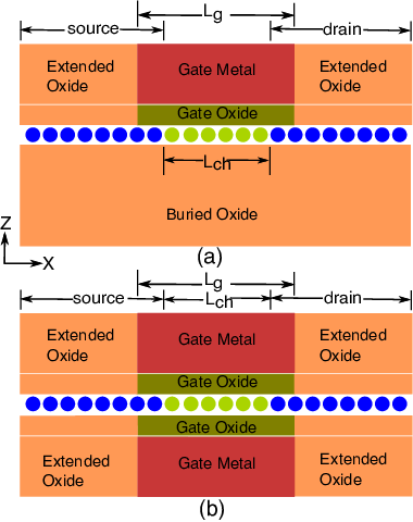
Figure 1 shows the device structures used for the simulations in this work [36]. The buried oxide and extended oxide regions are SiO2 with a dielectric constant of 3.9. The gate oxide is composed of both high-K (according to Table I) oxide under the gate and SiO2 [37] in the source-drain extensions for improved gate control. For the Si FET, transport from source to drain is in the (100) direction. For the BP FET, transport is in the direction, the direction of the light mass. For the circuit metrics, the default width of 4 times the pitch is used for the FETs [35].
For the TMD and Si FETs, electron conduction is considered while for the BP FET, both electron and hole conduction are considered, since most recent experimental work focuses on hole transport [38]. For the vdW materials, the source and drain doping densities were swept from to cm-3 ( cm-2). For each node and geometry, two results are recorded. One result is for the doping density that results in the maximum drive current. The second result is for the maximum doping density of cm-3. The drive currents versus source doping are shown in Fig. S1 of the Supplementary Information. This optimization is performed with the contact resistance set to zero. For the 3 nm Si UTB FETs, a source and drain doping density of cm-3 ( cm-2) is used [19].
Material properties for all of the materials considered in this work are summarized in Table S1 of the Supplementary Information. The UTB Si has a finite thickness of 3 nm, and all of the vdW materials are monolayers. It has been shown that adding multiple layers on top of a single layer cannot boost the on current [24]. Listed mobilities for monolayer vdW materials are experimentally measured values obtained from the literature [39, 40, 41, 7, 42, 43] except for MoTe2. Mobility in monolayer MoTe2 was unknown at the time of this work, hence it was approximated from MoSe2 using both materials’ electron effective masses (see footnote of table S1).
As evident from the conduction band -valley to -valley energy separation, , listed in Table S1, all values of are less than , and, therefore they will have an effect on the electron transport in the TMD FETs. Also, there is considerable spin-splitting in many of the conduction band and valleys. Therefore, we have taken the different spins and valleys into account by using a multiple single-band approach as depicted in Figure 2. In this approach, each spin and valley is treated as an independent band with its own effective mass.
For each band, the discretized effective mass Schrödinger equation is solved for the charge density using a non-equilibrium Green function (NEGF) approach similar to that described in [19]. The heavily doped source and drain regions are treated as contacts in equilibrium with their respective Fermi levels [44]. The total charge at each site is the sum of the charge calculated for each band. The charge is self-consistently solved with Poisson’s equation. The electrostatic potential within the device is calculated using a 2D finite difference solution of Poisson’s equation discretized on a 0.2 nm grid within the channel and a 0.5 nm grid within the oxide. Dirichlet boundary conditions are set at the metal gate and Von Neumann boundary conditions are used at all other exterior boundaries.
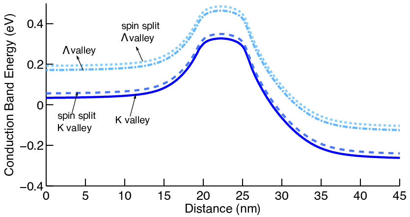
Once the charge calculation has converged, current is calculated for each band. The contribution from all bands is summed to give the total current. The effect of scattering in the channel is included with a reflection coefficient determined from a mean free path related to the mobility and an effective channel length [45, 46]. Details are provided in the Supplementary Information.
The off current is set at 1.5 for all devices. The drain bias , and on-state gate voltage are 0.3 V. The maximum allowable source-drain total contact resistances () are estimated following the methodology used by the ITRS [32, 36]. For this, a reference value of current was first calculated with scattering included but set to 0. A set of simulations including scattering were then performed for a range of values. was divided equally between the source and drain. In the self-consistent loop, the internal gate and drain potentials with respect to the source, and , were updated at each iteration according to and , where is the applied gate voltage with respect to ground. The series resistance raises the source potential by which lowers the gate to source voltage by the same amount. The particular value of that resulted in a 33.3% reduction of current compared to the reference current was then chosen as the maximum allowable contact resistance for the LV devices.
Two performance metrics are the switching delay and the switching energy defined as
| (1) |
Here, is the on-current, is the total capacitance that includes the oxide capacitance, the semiconductor capacitance (also known as quantum capacitance), and any parasitic capacitance that might be present. The capacitance is determined as follows. The total capacitance where is the total charge in the entire semiconductor region that includes the source, channel and drain. In this manner, the gate and fringing capacitances are taken into account all at the same time. In doing so, one has to make sure that no other external inputs are changing except the applied gate bias. Therefore, the total charge is calculated with = 0, since alters the effective gate voltage .
The calculated drive currents and capacitances are input into the BCB 3.0 scripts [35]. The BCB 3.0 scripts use the input for one type of transistor and approximate the on-current of the pFET is equal to that of the nFET. Delay times and switching energies are calculated using empirical rules chosen to match SPICE simulations. For circuits, a per unit length interconnect capacitance of 126 aF/m is used, and the interconnect length associated with each transistor is where is the DRAM half pitch corresponding to the technology node. Full details of the BCB 3.0 method are given in Ref. [35].
III Results
| 13.3 nm | 5.9 nm | ||||||||
|---|---|---|---|---|---|---|---|---|---|
| MoS2 | SG | 63.14 | 20.35 | 3 | 1.68 | 56.86 | 25.21 | 3 | 1.2 |
| DG | 107.1 | 33.6 | 6 | 0.9 | 110.2 | 48.06 | 5 | 0.6 | |
| MoSe2 | 61.81 | 17.89 | 4 | 1.8 | 56.8 | 22.75 | 3 | 1.28 | |
| MoTe2 | 61.7 | 16.9 | 4 | 1.9 | 55 | 21.16 | 3 | 1.57 | |
| WS2 | SG | 64.6 | 27.18 | 3 | 1.1 | 62 | 30.44 | 2 | 1.03 |
| DG | 109.8 | 45.18 | 4 | 0.63 | 113.2 | 56.9 | 4 | 0.5 | |
| WSe2 | SG | 67.6 | 29.67 | 3 | 1.02 | 64.85 | 34.2 | 2 | 0.83 |
| DG | 116 | 50.23 | 4 | 0.53 | 116.56 | 62.5 | 5 | 0.43 | |
| BP(N) | SG | 70.65 | 26.14 | 3 | 1.18 | 58.94 | 26.91 | 2.1 | 1.11 |
| DG | 121.6 | 42.08 | 4 | 0.76 | 111.15 | 50.95 | 4 | 0.6 | |
| BP(P) | SG | 75.8 | 33.45 | 2.55 | 0.95 | 59.2 | 30.55 | 2 | 0.95 |
| DG | 123.4 | 53.26 | 4 | 0.54 | 113.5 | 58.4 | 4 | 0.53 | |
| Si | SG | 19.7 | 9.73 | 1 | 2.9 | 6.22 | 3.73 | 1 | 6.5 |
| DG | 77.25 | 36 | 1 | 0.87 | 45.46 | 25.07 | 1 | 1.1 | |
The on-current, optimum doping, and series resistance for each material, node, and geometry are tabulated in Table II. refers to the ballistic on-current calculated with both the contact resistance and the backscattering coefficient set to 0. is the maximum allowable total contact resistance (source plus drain) that degrades the current calculated in the presence of scattering by 33.3%. is the on-current where both and the maximum allowable are included. For the rest of our discussion, unless otherwise noted, the on-current will refer to the scattering limited current, .

For the SG vdW materials, the drive currents at optimum doping are shown in Fig. 3 plotted versus the bandedge effective mass of the material for both the 2019 and the 2028 nodes. The inset is the same plot but for a fixed doping of cm-3. Each data point is labeled with its material.
The physical mechanisms governing FET performance are the same as those analyzed in Ref. [47] for III-V FETs, the balance between source exhaustion and tunneling leakage. The range of transport effective masses, from for p-type BP to for MoTe2, make this balance different for the different materials. The optimum source doping is lower for the lighter mass materials. The lower doping results in longer screening lengths of the channel potential into the source and the drain regions increasing the effective channel length and decreasing the off-state direct tunneling.
For the X-directed transport in p-type BP, the low mass in the transport direction provides a high velocity, and the large transverse effective mass provides many modes for transport. Because of the low transport mass, the optimum source doping of cm-3 is the lowest among the vdW FETs. As shown in Fig. 4, in the off-state, the low doping results in long screening lengths of the channel potential into the source and the drain regions increasing the effective off-state channel length and decreasing the off-state direct tunneling. The off-state channel potential decays approximately 10 nm into the source and 15 nm into the drain giving an off-state total effective source to drain length of 30 nm at the 2028 node. In the on-state, the small channel potential decays within a few nanometers into the source, and the high field region extends approximately 10 nm into the drain. Thus, the effective source to drain region in the on-state is approximately 15 nm. One advantage is that the longer depletion lengths in the source and drain reduce the fringing capacitance between the source and drain and therefore reduce the RC delay time. A disadvantage is that the transit time increases. A saturation velocity of cm/s gives a transit time that is 10 times less than the RC delay time. At cm/s, the two times are comparable.

As the gate length is scaled from 13 nm to 6 nm, with optimized doping, the on-current of BP drops slightly, and the on-currents of all of the TMD FETs increase. The TMD FETs with the heavier effective masses benefit from scaling, while the BP FET with the lightest transport mass is degraded by the scaling. In every case, the ballistic current decreases as the channel length decreases from 13 nm to 6 nm, in agreement with previous work [36], and the ballistic current of p-type BP with the lightest transport mass decreases the most. For BP, the large decrease in the ballistic current dominates, and the total current including scattering decreases. For the heavier mass TMDs, the ballistic current is only slightly reduced. As the channel length becomes comparable to the mean free path, reflection is reduced. This process dominates for the TMDs with heavier effective masses, and their on-current increases as the gate length is scaled down to 6 nm.
The effective mass affects two processes that determine if the current will increase or decrease with scaling, and the trends become very clear with a fixed source and drain doping of cm-3 as shown in the inset of Fig. 3. The first process is direct tunneling through the channel, and the second process is scattering in the channel. The process of direct tunneling is governed by the effective mass of the channel material. A heavier mass minimizes the off-state leakage which enhances the drive current for a fixed , because a smaller percentage of is required to shut the device off. This effect is illustrated in Fig. 5. The background color indicates the current spectrum (on a log scale) with the brightest yellow indicating the highest current. A comparison of Figs. 5(a) and (b) shows that, in the off-state, tunneling is significant through the BP barrier but is suppressed in the MoTe2 barrier. For BP with the lightest transport mass, the barrier height required to attain the off-state current of 1.5 nA/m is 365 meV. For MoTe2 with the heaviest transport mass, the barrier height required to attain the same off-state current is 307 meV, approximately 60 meV lower than that for BP. Applying 0.3 V to the gate reduces the potential in the channels by 254 meV for BP and 247 meV for MoTe2, so that the barrier height in the on-state is 111 meV for BP and 60 meV for MoTe2. Thus, the barrier height of the channel in the on-state for BP is almost twice that for MoTe2. This effect is responsible for the reduction in as the gate length is scaled from 13 nm to 6 nm.
The second process of scattering in the channel is also strongly correlated with the effective mass. A heavy mass is associated with a short mean free path, so that as the channel is scaled down to 6 nm, the device becomes more ballistic, decreases, and the current increases with scaling. The Mo compounds have the highest effective masses, the lowest measured electron mobilities, and the shortest mean free paths as shown in Table S1. Therefore, these materials benefit most from scaling, since direct leakage through the channel is not a problem, and they become more ballistic as the channel length is scaled. For BP with the lightest mass in the transport direction, the first process of tunneling dominates the performance, and there is significant reduction in going from the 2019 to the 2028 node when the doping is fixed at cm-3. Even at the optimum doping condition, BP is the only 2D material that suffers from a reduction in current after scaling.

Adding a second gate to create a DG structure increases the magnitude of the current, and the increase in the magnitude of the current is qualitatively different for the vdW channels and the UTB Si channel. At the 2019 node, adding a second gate increases by a factor of 1.7 for the TMD FETs and 1.63 for p-type BP. The increase in is slightly less. For 2028 TMDs, adding the second gate increases by factors of 1.8 - 1.94 for TMDs and 1.9 for both BP. The increase in is identical to the increase in within numerical error. The larger increases in current due to doubling the gates in the 2028 2D FETs indicate that the single gate is losing some control of the channel when the gate is scaled down to 5.9 nm. In the DG geometry, the second gate provides greater electrostatic control of the channel. The increased gate control moves the position where further towards the drain which increases and, consequently, , and is the reason why the increase in resulting from a second gate may not be quite as large as the increase in .
The maximum allowable projected total contact resistance (source plus drain) for each node and material are also included in Table II. For the SG devices, the current is small, and one can get away with relatively high contact resistances on the order of 0.48 to 0.95 km per contact at the 2019 node, and 0.42 to 0.52 km per contact at the 2028 node. To achieve the higher current densities of the DG TMD devices, lower contact resistances are required, on the order of 265 - 450 m per contact at 2019 node and 215 - 300 m per contact at 2028 node. Contact resistances of 240 m have already been reported in literature [48].
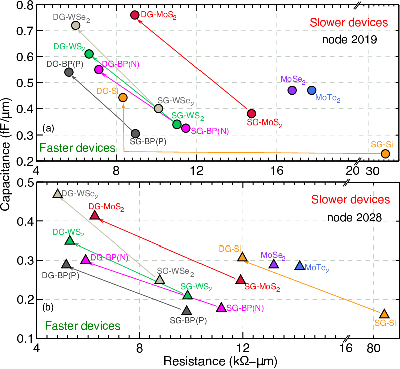
From Eq. (1), the product of device capacitance and resistance gives the switching delay of each individual device. Fig. 6 shows the capacitance versus resistance for each material, node, and geometry. The arrows show the effect of going from a SG geometry to a DG geometry. First, we discuss the SG geometry at each node. At the 2019 node, among the SG vdW FETs, MoSe2 and MoTe2 have both the most resistance and capacitance and BP has the least. At the 2028 node, among the SG vdW FETs, WSe2 has the smallest resistance among all the vdW materials since it has the highest drive current, and BP has the lowest capacitance. To understand the low capacitance, recall that the ‘device’ capacitance is determined by . Therefore, if the device is only weakly turned on, there is little charge in the channel, and is small, irrespective of the actual geometrical gate capacitance. Considering the band diagram of BP at the 2028 node in Fig. 4, it is weakly turned on since the top of the barrier is 83 meV above the source Fermi level. In comparison, MoTe2 with the heaviest mass is more strongly turned on, and its capacitance is the highest even though its current is the lowest among the vdW FETs. Its low current or high resistance result from the low mobility and short mean free paths.
Both the 2028 SG and DG Si FETs stand out in Fig. 6. Applying a DG to 2028 UTB Si gives a capacitance that is slightly below the DG vdW FET using p-type BP. There are several reasons for the low capacitance of the Si DG FET. The 3 nm thick channel requires a double gate to accumulate significant charge in the channel and turn the device on. Even when charge is accumulated in the channel, the relatively lower effective mass of the lowest quantized state in the channel of 0.22 results in a lower quantum capacitance [19]. Finally, the lower doping of the source and drain of cm-3 compared to the doping of the DG vdW FETs of cm-3 - cm-3 results in longer depletion regions in the source and drain that reduce the fringing capacitance for the sidewalls of the gates. The UTB Si band diagrams shown in Fig. S3 illustrate these points.
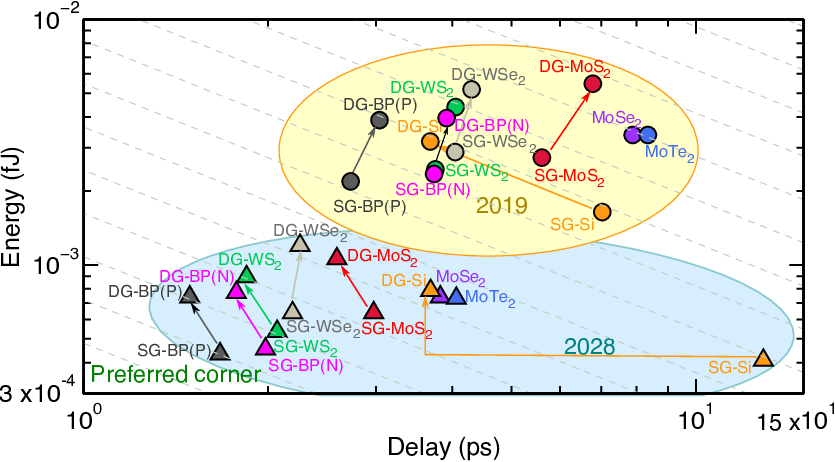
The intrinsic switching energies versus switching delay times are shown in Fig. S4. At node 2019, the SG WS2 and WSe2 FETs and DG-Si have very similar switching energies and delay times. Adding a second gate to the 2D materials is detrimental in all cases causing both the energy and delay to increase. At the 2028 node, adding a second gate still moves all of the 2D materials to a higher energy-delay product. Only Si is moved to a lower energy-delay product by the addition of a second gate.
Energy-delay benchmarks for a 32 bit adder are shown in Fig. S5. Now, the added capacitance of the interconnects is included. For a per unit length capacitance of 126 aF/m, the interconnect capacitance per transistor is aF at the 2019 node and 18 aF at the 2028 node. The default widths used for the FETs are 4 times the pitches, and they are 80 nm at the 2019 node and 28.4 nm at the 2028 node. Multiplying these widths times the capacitance values in Fig. 6 gives the actual FET capacitances. For the vdW FETs, at the 2019 node, ranges between 1.33 - 2.05 times the SG-FET capacitances and between 0.82 - 1.16 times the DG-FET capacitances. At the 2028 node, ranges between 2.18 - 3.73 times the SG-FET capacitances and between 1.35 - 2.18 times the DG-FET capacitances. The interconnect contribution to the delay depends on the current that flows through the interconnect, and this current is the same as the device current. As a result, the drive current becomes more important for the performance of circuits. For a SG-TMD FET at either the 2019 or 2028 node, adding a second gate increases the intrinsic device switching energy more than it decreases the delay, so that the device energy-delay product increases. This same trend applies to the 2019 circuit. However, for the 2028 circuit, adding a second gate leaves the energy-delay product almost unchanged for BP, WS2 and MoS2 and slightly increased for WSe2.

The power density as a function of computational throughput is shown in Fig. S6. Computational throughput is defined as number of integer operations per second per unit area (32 bit additions in the case of 32 bit adder) [34]. The throughput is the inverse of the circuit delay time in Fig. S5 divided by the circuit area. Since the areas for all adders at a given node are taken to be the same, the throughput is proportional to the inverse of the adder delay time. At the 2028 node, SG WSe2, WS2, and BP all have significantly higher throughputs than DG-Si with slightly higher power density. Following Refs. [34] and [35], we set the power density limit to 10 W/cm2. All of the FETs lie within the power density constraints since they all operate at low voltage (0.3 V).

IV Summary and Conclusions
We performed quantum mechanical simulations for vdW FETs with monolayer MoS2, MoSe2, MoTe2, WS2, WSe2, and BP channels operating in the LV regime for geometries corresponding to those of the 2019 node and the 2028 node of the 2013 ITRS. A UTB Si FET was simulated using the same approach to provide a comparison. The FET serves as a baseline device for determining targets for material parameters. As the gate length is scaled from 13.3 nm to 5.9 nm, blocking the leakage current becomes more critical, and the TMD materials with the heavier effective masses benefit most from extreme scaling. For all materials, the ballistic current always reduces with scaling in agreement with previous work [36]. However, the full current that includes the effect of scattering can either increase or decrease, and the increase or decrease is governed by two competing processes that are both closely tied to the effective mass, direct tunneling through the channel and backscattering from the channel. There is an optimum effective-mass of corresponding to that of WSe2 that provides a maximum drive current for LV operation with V. The short 6 nm gate length combined with LV operation is forgiving in its requirements for material quality and contact resistances. Low-voltage results in low current and thus low IR drop across the contact resistances, and the short 6 nm gate length becomes less than the mean free path of the low-mobility material. At the 2028 node, the single gate vdW FETs show competitive performance in terms of drive current and power density. These performance metrics are obtained using currently measured values for mobilities shown in Table S1 and contact resistances shown in Table II that are comparable to the best measured contact resistances [48].
Supplementary Material
Table S1 provides the material parameters used in the calculations described in Sec. II of the paper. The measured mobility in monolayer MoTe2 was unknown at the time of this work, hence was calculated as . During the review process, we became aware of measurements on multilayer MoTe2 flakes showing a room temperature mobility of approximately 21 [50]. Since TMDs are weakly coupled van der Waals layers, these mobility values can be representative of monolayer mobility as well [51] (or an upper bound). One caveat with these values is that the devices were not encapsulated during measurements and hence the mobility values represent a lower bound. A mobility value of 21 (in contrast to 42.74 as used in this work) would shorten the mean free path further and degrade the overall performance for MoTe2. For Si, we followed Ref. [52] and used a mobility of 200 which could be considered as an optimistic value, since at lower inversion charge densities, mobilities can be reduced by a factor 2 [53].
Fig. S1 shows how the drive currents vary as a function of the source and drain doping densities. The doping densities that gave the maximum drive currents (in the absence of contact resistance) were chosen. At the highest doping of cm-3, the Fermi level lies close to the band edge for all of the vdW materials. The source (and drain) degeneracy () varies between -21.65 meV to 10.5 meV for the vdW materials where is the source Fermi energy and () are the source conduction (valance) band edges. Even though the source doping of Si is one order of magnitude less than the highest doping used for the TMD FETs, the source degeneracy of the Si Fermi level, meV, is the largest among all of the FETs. This is a result of its density of states mass () times its degeneracy, 2 orbitals and 2 spins, being the smallest. For comparison, BP has the smallest transport mass, but, because of its huge anisotropy, its density of states masses of for hole and for electron are large.
While source exhaustion sets the lower limit on the doping in an unconstrained layout, there are design rules that limit the extent of the depletion regions into the source and drain. The source and drain depletion lengths will be terminated at the vias for the metal 1 contacts to the source and drain. Following the layout of Fig. 26 in Ref. [34], for the 2028 node, these regions will be 7.1 nm to the left and right of the physical gate limiting the depletion lengths to 7.1 nm into the source and drain. To determine whether the layout constraint at the 2028 node affects the performance trends, we simulate the SG p-type BP and WSe2 FETs with doping in the via regions on the left and right side of the gate with optimized doping between the via and the gate. The value of the optimum doping does not change, and the band diagrams for the p-type BP FET with and without the heavily doped via are shown in Fig. S2. The currents for both the WSe2 FET and the BP FET slightly decrease. For WSe2, Am, and Am. For p-type BP, Am, and Am. In both cases decreases more than . The reason is that in the on-state, there is a stronger pull on the channel from the heavily doped drain via that drives the point at which the channel potential drops by back towards the source. This reduces the effective channel length, , which reduces the backscattering coefficient . Since the trends and relative performance are not affected by the proximity of the via we did not consider it in the main text.
For 2019 UTB Si, going to a DG structure increases by a factor of 3.9 and by a factor of 3.7 compared to their values in the SG geometry. For 2028 UTB Si, going to a DG structure increases by a factor of 7.3 and by a factor of 6.7 compared to their values in the SG geometry. The much larger increases in the UTB Si currents going from a SG to a DG geometry at the 2028 node compared to those of the 2D material currents are a result of the different channel thicknesses. At the 2028 node, a double gate is required to control the potential through the 3 nm Si channel. This is illustrated in Fig. S3. The set of green curves in Fig. S3 shows the conduction band edges for SG Si at each grid point through the depth of the Si channel. The highest curves are at the top of the channel adjacent to the gate oxide, and the lowest curves are at the bottom of the channel adjacent to the substrate. The large spread in energy of the curves illustrates the loss of control of the channel potential by the single gate. The set of blue curves show the same set of conduction band edges for the DG device. The double gate provides good control of the potential throughout the channel. For the thinner monolayer vdW FETs, a single gate is adequate.
NEGF Details
The heavily doped source and drain regions are treated as contacts in equilibrium with their respective Fermi levels [44], and the charge in those regions is calculated from the equilibrium expression,
| (2) |
where is the band index, is the spin degeneracy and is the valley degeneracy which is 2 for the -valleys, 6 for the -valleys and 1 for the -valley. is the effective mass in the width direction, is Boltzmann’s constant, is temperature, and is the spectral function on site for band given by . The factors are the reduced Fermi factors resulting from analytically integrating over the transverse momentum where is the Fermi level of the source (drain), respectively. Within the device region, the charge is calculated from the non-equilibrium expression,
| (3) |
where is the source (drain) connected spectral function at site for band , given by and .
The drain current is calculated within the self-consistent loop from
| (4) |
where is the transmission coefficient for band , and is the backscattering coefficient, [45]. is the critical length determined by the distance from top of the barrier in the channel to the position towards the drain where the potential drops by . The mean free path is calculated using [46]
| (5) |
where is the thermal velocity and .
The same equations are used for the UTB Si FET. The discretization within the 3 nm thick channel is 0.2 nm in the direction and 0.25 nm in the direction as shown in Fig. 1 of the main article. The charge is calculated everywhere using the non-equilibrium expression, Eq. (3).
| Material | MoS2 | MoSe2 | MoTe2 | WS2 | WSe2 | BP | Si |
| Bandgap (eV) | 1.67 | 1.40 | 0.997 | 1.60 | 1.30 | 1.55 | 1.12 |
| Thickness (nm) | 0.65 | 0.73 | 0.7 | 0.62 | 0.73 | 0.57 | 3 |
| Measured mobility, | 81 | 50 | 42.74† | 185 | 202 | = 94 | 200 |
| = 116 | |||||||
| Effective | =0.43 | =0.49 | =0.53 | =0.35 | =0.39 | ||
| mass, | =0.46 | =0.56 | =0.62 | =0.26 | =0.28 | ||
| =0.56 | =0.48 | =0.43 | =0.52 | =0.42 | |||
| =1.13 | =1.08 | =0.99 | =0.74 | =0.74 | |||
| =0.64 | =0.54 | =0.42 | =0.69 | =0.73 | |||
| =1.21 | =1.11 | =1.16 | =0.94 | =0.91 | |||
| CB -valley | 3 | 22 | 36 | 32 | 37 | ||
| spin-splitting (meV) | |||||||
| CB -valley | 70 | 21 | 22 | 264 | 218 | ||
| spin-splitting (meV) | |||||||
| CB (meV) | 207 | 137 | 158 | 81 | 35 | ||
| Mean free path, | = 5.2 | = 3.4 | = 3.1 | = 10.7 | = 12.3 | = 11.1 | 9 |
| (nm) (approx.) | = 5.3 | = 3.6 | = 3.3 | = 9.1 | = 10.3 | = 6.1 | |
| = 7 | = 4.1 | = 3.3 | = 14 | = 14.5 | |||
| = 7.3 | = 4.2 | = 3.4 | = 16 | = 17.5 | |||
| †Measured mobility in monolayer MoTe2 was unknown, hence is calculated as: | |||||||


References
- [1] K. Galatsis, C. Ahn, I. Krivorotov, P. Kim, R. Lake, K. L. Wang, and J. P. Chang, “A Material Framework for Beyond-CMOS Devices,” IEEE Journal on Exploratory Solid-State Computational Devices and Circuits, vol. 1, pp. 19–27, Dec 2015.
- [2] B. Radisavljevic, A. Radenovic, J. Brivio, V. Giacometti, and A. Kis, “Single-layer MoS2 transistors,” Nat Nano, vol. 6, no. 3, pp. 147–150, 3 2011.
- [3] A. Kormányos, G. Burkard, M. Gmitra, J. Fabian, V. Zólyomi, N. D. Drummond, and V. Fal’ko, “kp theory for two-dimensional transition metal dichalcogenide semiconductors,” 2D Materials, vol. 2, no. 2, p. 022001, 2015.
- [4] S. Larentis, B. Fallahazad, and E. Tutuc, “Field-effect transistors and intrinsic mobility in ultra-thin MoSe2 layers,” Applied Physics Letters, vol. 101, no. 22, 2012.
- [5] Z. Huang, W. Zhang, W. Zhang, and Y. Li, “Screening for two dimensional mx semiconductors with possible high room temperature mobility,” arXiv preprint arXiv:1505.05698, 2015.
- [6] Q. H. Wang, K. Kalantar-Zadeh, A. Kis, J. N. Coleman, and M. S. Strano, “Electronics and optoelectronics of two-dimensional transition metal dichalcogenides,” Nat Nano, vol. 7, no. 11, pp. 699–712, 11 2012.
- [7] W. Liu, J. Kang, D. Sarkar, Y. Khatami, D. Jena, and K. Banerjee, “Role of Metal Contacts in Designing High-Performance Monolayer n-Type WSe2 Field Effect Transistors,” Nano Letters, vol. 13, no. 5, pp. 1983–1990, 2013.
- [8] H. Fang, S. Chuang, T. C. Chang, K. Takei, T. Takahashi, and A. Javey, “High-Performance Single Layered WSe2 p-FETs with Chemically Doped Contacts,” Nano Letters, vol. 12, no. 7, pp. 3788–3792, 2012.
- [9] S. Fathipour, N. Ma, W. S. Hwang, V. Protasenko, S. Vishwanath, H. G. Xing, H. Xu, D. Jena, J. Appenzeller, and A. Seabaugh, “Exfoliated multilayer MoTe2 field-effect transistors,” Applied Physics Letters, vol. 105, no. 19, 2014.
- [10] L. Li, Y. Yu, G. J. Ye, Q. Ge, X. Ou, H. Wu, D. Feng, X. H. Chen, and Y. Zhang, “Black phosphorus field-effect transistors,” Nat Nano, vol. 9, no. 5, pp. 372–377, 2014.
- [11] H. Liu, A. T. Neal, Z. Zhu, Z. Luo, X. Xu, D. Tománek, and P. D. Ye, “Phosphorene: An unexplored 2d semiconductor with a high hole mobility,” ACS Nano, vol. 8, no. 4, pp. 4033–4041, 2014.
- [12] F. Xia, H. Wang, and Y. Jia, “Rediscovering black phosphorus as an anisotropic layered material for optoelectronics and electronics,” Nat Commun, vol. 5, 7 2014.
- [13] J. Qiao, X. Kong, Z.-X. Hu, F. Yang, and W. Ji, “High-mobility transport anisotropy and linear dichroism in few-layer black phosphorus,” Nat Commun, vol. 5, 2014.
- [14] K.-T. Lam, Z. Dong, and J. Guo, “Performance limits projection of black phosphorous field-effect transistors,” Electron Device Letters, IEEE, vol. 35, no. 9, pp. 963–965, 2014.
- [15] A. Castellanos-Gomez, “Black phosphorus: narrow gap, wide applications,” arXiv preprint arXiv:1508.00874, 2015.
- [16] X. Ling, H. Wang, S. Huang, F. Xia, and M. S. Dresselhaus, “The renaissance of black phosphorus,” Proceedings of the National Academy of Sciences, vol. 112, no. 15, pp. 4523–4530, 2015.
- [17] Y. Yoon, K. Ganapathi, and S. Salahuddin, “How good can monolayer MoS2 transistors be?” Nano letters, vol. 11, no. 9, pp. 3768–3773, 2011.
- [18] L. Liu, Y. Lu, and J. Guo, “On monolayer field-effect transistors at the scaling limit,” Electron Devices, IEEE Transactions on, vol. 60, no. 12, pp. 4133–4139, 2013.
- [19] K. Alam and R. K. Lake, “Monolayer MoS2 Transistors Beyond the Technology Road Map,” Electron Devices, IEEE Transactions on, vol. 59, no. 12, pp. 3250–3254, 2012.
- [20] S. M. Tabatabaei, M. Noei, K. Khaliji, M. Pourfath, and M. Fathipour, “A first-principles study on the effect of biaxial strain on the ultimate performance of monolayer MoS2-based double gate field effect transistor,” Journal of Applied Physics, vol. 113, no. 16, p. 163708, 2013.
- [21] Á. Szabó, R. Rhyner, and M. Luisier, “Ab initio simulation of single-and few-layer MoS2 transistors: Effect of electron-phonon scattering,” Physical Review B, vol. 92, no. 3, p. 035435, 2015.
- [22] J. Chang, L. F. Register, and S. K. Banerjee, “Atomistic full-band simulations of monolayer MoS2 transistors,” Applied Physics Letters, vol. 103, no. 22, p. 223509, 2013.
- [23] A. Sengupta, R. K. Ghosh, and S. Mahapatra, “Performance Analysis of Strained Monolayer MOSFET,” Electron Devices, IEEE Transactions on, vol. 60, no. 9, pp. 2782–2787, 2013.
- [24] V. Mishra, S. Smith, L. Liu, F. Zahid, Y. Zhu, H. Guo, and S. Salahuddin, “Screening in Ultrashort (5 nm) Channel MoS2 Transistors: A Full-Band Quantum Transport Study,” Electron Devices, IEEE Transactions on, vol. 62, no. 8, pp. 2457–2463, 2015.
- [25] K. Majumdar, C. Hobbs, and P. D. Kirsch, “Benchmarking transition metal dichalcogenide MOSFET in the ultimate physical scaling limit,” Electron Device Letters, IEEE, vol. 35, no. 3, pp. 402–404, 2014.
- [26] L. Liu, S. B. Kumar, Y. Ouyang, and J. Guo, “Performance limits of monolayer transition metal dichalcogenide transistors,” Electron Devices, IEEE Transactions on, vol. 58, no. 9, pp. 3042–3047, 2011.
- [27] J. Chang, L. F. Register, and S. K. Banerjee, “Ballistic performance comparison of monolayer transition metal dichalcogenide MX2 (M = Mo, W; X = S, Se, Te) metal-oxide-semiconductor field effect transistors,” Journal of Applied Physics, vol. 115, no. 8, 2014.
- [28] H. Ilatikhameneh, Y. Tan, B. Novakovic, G. Klimeck, R. Rahman, and J. Appenzeller, “Tunnel field-effect transistors in 2-d transition metal dichalcogenide materials,” Exploratory Solid-State Computational Devices and Circuits, IEEE Journal on, vol. 1, pp. 12–18, Dec 2015.
- [29] K.-T. Lam, X. Cao, and J. Guo, “Device performance of heterojunction tunneling field-effect transistors based on transition metal dichalcogenide monolayer,” Electron Device Letters, IEEE, vol. 34, no. 10, pp. 1331–1333, 2013.
- [30] F. Liu, Y. Wang, X. Liu, J. Wang, and H. Guo, “Ballistic transport in monolayer black phosphorus transistors,” Electron Devices, IEEE Transactions on, vol. 61, no. 11, pp. 3871–3876, 2014.
- [31] H. Ilatikhameneh, T. Ameen, B. Novakovic, Y. Tan, G. Klimeck, and R. Rahman, “Saving moore’s law down to 1nm channels with anisotropic effective mass,” arXiv preprint arXiv:1605.03979, 2016.
- [32] “International Technology Roadmap for Semiconductors,” 2013, [online]. Available: http://www.itrs.net.
- [33] U. E. Avci, R. Rios, K. Kuhn, and I. A. Young, “Comparison of performance, switching energy and process variations for the TFET and MOSFET in logic,” in VLSI Technology (VLSIT), 2011 Symposium on, June 2011, pp. 124–125.
- [34] D. Nikonov and I. Young, “Overview of Beyond-CMOS Devices and a Uniform Methodology for Their Benchmarking,” Proceedings of the IEEE, vol. 101, no. 12, pp. 2498–2533, Dec 2013.
- [35] D. Nikonov and I. Young, “Benchmarking of Beyond-CMOS Exploratory Devices for Logic Integrated Circuits,” Exploratory Solid-State Computational Devices and Circuits, IEEE Journal on, vol. 1, pp. 3–11, April 2015.
- [36] M. Salmani-Jelodar, S. Kim, K. Ng, and G. Klimeck, “Transistor roadmap projection using predictive full-band atomistic modeling,” Applied Physics Letters, vol. 105, no. 8, p. 083508, 2014.
- [37] M. Luisier, M. Lundstrom, D. A. Antoniadis, and J. Bokor, “Ultimate device scaling: Intrinsic performance comparisons of carbon-based, InGaAs, and Si field-effect transistors for 5 nm gate length,” in Electron Devices Meeting (IEDM), 2011 IEEE International, dec. 2011, pp. 11.2.1 –11.2.4.
- [38] H. Du, X. Lin, Z. Xu, and D. Chu, “Recent developments in black phosphorus transistors,” Journal of Materials Chemistry C, vol. 3, no. 34, pp. 8760–8775, 2015.
- [39] Z. Yu, Y. Pan, Y. Shen, Z. Wang, Z.-Y. Ong, T. Xu, R. Xin, L. Pan, B. Wang, L. Sun, et al., “Towards intrinsic charge transport in monolayer molybdenum disulfide by defect and interface engineering,” Nature communications, vol. 5, 2014.
- [40] X. Wang, Y. Gong, G. Shi, W. L. Chow, K. Keyshar, G. Ye, R. Vajtai, J. Lou, Z. Liu, E. Ringe, et al., “Chemical vapor deposition growth of crystalline monolayer MoSe2,” ACS nano, vol. 8, no. 5, pp. 5125–5131, 2014.
- [41] M. W. Iqbal, M. Z. Iqbal, M. F. Khan, M. A. Shehzad, Y. Seo, J. H. Park, C. Hwang, and J. Eom, “High-mobility and air-stable single-layer WS2 field-effect transistors sandwiched between chemical vapor deposition-grown hexagonal BN films,” Scientific reports, vol. 5, 2015.
- [42] S. Das, W. Zhang, M. Demarteau, A. Hoffmann, M. Dubey, and A. Roelofs, “Tunable transport gap in phosphorene,” Nano letters, vol. 14, no. 10, pp. 5733–5739, 2014.
- [43] D. J. Perello, S. H. Chae, S. Song, and Y. H. Lee, “High-performance n-type black phosphorus transistors with type control via thickness and contact-metal engineering,” Nature communications, vol. 6, 2015.
- [44] G. Klimeck, R. Lake, R. C. Bowen, W. R. Frensley, and T. Moise, “Quantum device simulation with a generalized tunneling formula,” Appl. Phys. Lett., vol. 67, no. 17, pp. 2539–2541, 1995.
- [45] M. Lundstrom, “Elementary scattering theory of the Si MOSFET,” Electron Device Letters, IEEE, vol. 18, no. 7, pp. 361–363, 1997.
- [46] C. Jeong, D. A. Antoniadis, and M. S. Lundstrom, “On backscattering and mobility in nanoscale Silicon MOSFETs,” Electron Devices, IEEE Transactions on, vol. 56, no. 11, pp. 2762–2769, 2009.
- [47] R. Kim, U. E. Avci, and I. A. Young, “Source/Drain Doping Effects and Performance Analysis of Ballistic III-V n-MOSFETs,” J. Elect. Dev. Soc., vol. 3, no. 1, 2015.
- [48] R. Kappera, D. Voiry, S. E. Yalcin, B. Branch, G. Gupta, A. D. Mohite, and M. Chhowalla, “Phase-engineered low-resistance contacts for ultrathin MoS2 transistors,” Nature materials, vol. 13, no. 12, pp. 1128–1134, 2014.
- [49] An enlarged version of this figure is provided in the Supplementary Information.
- [50] Private communication, Prof. Emanuel Tutuc.
- [51] B. Fallahazad, H. C. Movva, K. Kim, S. Larentis, T. Taniguchi, K. Watanabe, S. K. Banerjee, and E. Tutuc, “Shubnikov–de haas oscillations of high-mobility holes in monolayer and bilayer wse 2: Landau level degeneracy, effective mass, and negative compressibility,” Physical review letters, vol. 116, no. 8, p. 086601, 2016.
- [52] R. Venugopal, M. Paulsson, S. Goasguen, S. Datta, and M. S. Lundstrom, “A simple quantum mechanical treatment of scattering in nanoscale transistors,” J. Appl. Phys., vol. 93, no. 9, pp. 5613–5625, 2003.
- [53] N. Xu, B. Ho, F. Andrieu, L. Smith, B.-Y. Nguyen, O. Weber, T. Poiroux, O. Faynot, and T.-J. King Liu, “Carrier-mobility enhancement via strain engineering in future thin-body mosfets,” IEEE electron device letters, vol. 33, no. 3, pp. 318–320, 2012.