Incipient Berezinskii-Kosterlitz-Thouless transition in two-dimensional coplanar Josephson junctions
Abstract
Superconducting hybrid junctions are revealing a variety of novel effects. Some of them are due to the special layout of these devices, which often use a coplanar configuration with relatively large barrier channels and the possibility of hosting Pearl vortices. A Josephson junction with a quasi ideal two-dimensional barrier has been realized by growing graphene on SiC with Al electrodes. Chemical Vapor Deposition offers centimeter size monolayer areas where it is possible to realize a comparative analysis of different devices with nominally the same barrier. In samples with a graphene gap below 400 nm, we have found evidence of Josephson coherence in presence of an incipient Berezinskii-Kosterlitz-Thouless transition. When the magnetic field is cycled, a remarkable hysteretic collapse and revival of the Josephson supercurrent occurs. Similar hysteresis are found in granular systems and are usually justified within the Bean Critical State model (CSM). We show that the CSM, with appropriate account for the low dimensional geometry, can partly explain the odd features measured in these junctions.
pacs
74.50.+r, 85.25.Cp, 74.45.+cI Introduction
Superconducting hybrid junctions can now be obtained combining superconductors with functional barriers as semiconductors [1], graphene[2, 3], topological insulators [4, 5], ferromagnets[6, 7] made superconducting by the proximity effect. These devices often use a coplanar layout with almost two-dimensional (2D) flakes or nanowires as barriers. [1, 8, 9, 10] The geometry of the device and the nature of the interfaces may favor the appearance of novel exotic effects ranging from Majorana fermions [11, 12] to topological superconductivity [5]. In this paper we will show how the emerging class of 2D extended barriers can promote Josephson coherence in presence of an incipient Berezinskii-Kosterlitz-Thouless [13, 14] transition, which is indeed, supposed to be a peculiarity of 2D superconducting systems. In this case a 2D barrier is made superconducting by proximity effect. To this aim we have realized graphene Josephson junctions (GJJs), obtained using a graphene barrier deposited on SiC by Chemical Vapor Deposition (CVD) rather than the standard technique of an exfoliated flake[15]. Graphene on SiC is highly homogeneous at the centimeter scale. Thus relatively simple lithography processes allow to obtain thousands of devices on the same wafer.[16] This specific type of graphene growth guarantees to have devices with the desired geometry, i.e. a 2D barrier of suitable lateral dimensions to host 2D vortex structures. Large graphene samples deposited as a thin film offers enough room to host extremely spread out 2D vortex entities. Vortex pinning is expected to occur because of interface impurities between the graphene sheet and the thin superconducting electrode.
In this paper we show how the Josephson coherence is observed along with very unusual features like the persistence of a small residual resistance and, even more surprising, the appearance of a hysteresis in magnetic field, manifesting in collapses and revivals of the supercurrent depending on the direction of the magnetic sweeping (see Fig. 4). This points to Josephson conduction in presence of an incipient Berezinskii-Kosterlitz-Thouless (BKT) transition at subKelvin temperature.
Our results are a fundamental step towards scalability for GJJs, and for our goals it offers the additional advantage of comparing junctions fabricated on exactly the same barrier. This can be extremely useful to have further insights on the electrodynamic response and the nature of dissipation of GJJs, which need to be considered in the actual rush of more performing devices in the ballistic limit, to exploit the unique properties of Andreev reflection in graphene.[17, 18, 19, 20, 21, 22, 23]
In Section II we report on the preparation of the sample. A consistent interpretation of the phenomenology described in Sections III–V requires frames which go beyond the usual Josephson S/N/S paradigm. The superconducting proximity is quite unique in our samples. The Josephson supercurrent is always accompanied by a small resistance, but it drops to a very low value very fast, as soon as a very weak orthogonal magnetic field is applied, apparently without loosing Josephson phase coherence. Meanwhile, the resistance increases from a few Ohms to values of the order of . The situation does not change if the field is further increased, but, as soon as we invert the sweeping direction at any magnetic field value below a threshold field, the Josephson supercurrent has an unexpected revival, in presence of a remanent magnetization. Simultaneously, the resistance drops again. All these observations are consistent with a special regime of the proximity effect, expected to occur only in two dimensions and in presence of pinning of vortices.
Similar hysteresis in the magnetization or in the critical current of granular systems is found in type II superconductors and is usually justified within the Bean Critical State model (CSM).[24] The CSM can provide a qualitative interpretation of the magnetization process, which takes place in the Al/Ti islands covering the graphene, and of the measured hysteresis. Support to this interpretation comes from the fact that metal decorated graphene sheets have been fabricated[25] and their superconducting phase transition has been classified as of the BKT type.[13, 14] Cooling down the devices below the critical temperature of the electrodes ( K) in zero field, apparently leads to incipient superconductivity in the graphene layer.
The plots of the resistance vs. temperature presented in Section III support a qualitative interpretation of the measured phenomena within the BKT theory (see Fig. 3) at low temperatures. In this regime vortex-antivortex (-) pair unbinding and flux-flow resistance across the junction are dominant phenomena. We have measured our samples down to mK which is a much higher temperature than the expected BKT critical temperature, . Features of the BKT incipient transition survive in the crossover to a paraconductivity regime at . The Josephson supercurrent modulated by the magnetic field is accompanied by the flow of vortices, which induces a finite slope in the supercurrent branch. An analysis of the flux flow resistance points to large Pearl vortices, pinned to the impurities in the CSM phase. Magnetic screening is very weak and correlations at intermediate distances induced by the long range repulsive interaction can be strong, particularly when the applied orthogonal magnetic field is very small. All of this is discussed in Sections IV and V.
In Section VI the Fraunhofer pattern of the Josephson conduction is discussed. By ignoring details of the microscopic vortex structure and dynamics, a macroscopic approach to the diamagnetic screening currents, based on the solution of the London equation in a quasi 2D contact, can reasonably account for the measured pattern if flux focusing effects are assumed in the planar thin-film weak link[26]. Sections VII and Section VIII contain a detailed summary and the conclusions, respectively.
II Sample preparation
The graphene layer was grown by CVD on the silicon face of a SiC substrate. The semi-insulating SiC substrate has an extremely small, negligible conductivity. The quality of the monolayer structure was carefully investigated by Raman and Angle Resolved Photo Emission Spectroscopy[15] (see Refs. 27, 28 for details). Before lithography, the mobility at room temperature is cm2/Vs. The graphene is -doped, cm-2. This -doping is induced by the hydrogenation of interface between graphene and SiC.[28]

The planar Josephson devices are fabricated by conventional -beam lithography. The graphene junctions are patterned by oxygen plasma. Then, the contacts are deposited (see Fig. 1). They consist of a 5 nm interfacial layer of titanium, which ensures good electrical contact to graphene, a 80 nm thick aluminium layer and a 3 nm thick gold layer. It has been reported that Al on top of graphene could induce a strong doping[29]. As the pristine graphene is initially -doped, these Al/graphene junctions could be suitable for fabricating -- junctions, with appropriate protocols which include gates. In our devices, the gap between the electrodes remains relatively large, ranging from 200 nm to 600 nm. The width of the junctions is fixed at m. Charge transport is most likely diffusive. Thus Fabry-Perot resonances and Klein tunnelling are not expected to be present.
These junctions have a major difference with graphene junctions obtained by the exfoliation technique. While the geometrical junction area is , here the remaining graphene area below the superconducting Al contacts is massive. On purpose, we left a graphene area m2 under each of the two Al contacts. A part of these areas is visible in Fig. 1a. For the measurements, the samples are thermally anchored to the cold stage of a 3He cryostat equipped with EMI filters at room temperature, RC filters at the 1-K pot stage and copper powder filters at the sample stage [30, 31]. Current-voltage (I-V) characteristics of different junctions have been measured as a function of temperature and magnetic field. Measurements of resistance as a function of temperature, , and magnetic field, , have been performed with standard low frequency lock-in techniques using low excitation currents, in the range 5–10 nA.
Table 1 collects measured and fitted parameters of some of the studied junctions. For the shortest junction (J200-4, nm), the I-V curves are reported at various temperatures in Fig. 2. We measure a finite slope in the I-V characteristics close to zero voltage, even at the lowest temperatures. The linear part is followed by a bending which is characteristic of the resistively shunted junction (RSJ) model. The critical current as a function of an externally applied magnetic field is estimated through the RSJ model (see inset of Fig. 2), suitably used for an overdamped Josephson junction [32] in series with a resistance. We attribute the finite slope in the supercurrent branch to the presence of fluctuating broken vortex-antivortex pairs which cannot be described appropriately within the RSJ framework or more refined arguments based on phase diffusion [30, 31, 32, 33] (see Sections IV and V). Indeed, our RSJ fit points to an effective temperature which is larger than the base temperature.
III Temperature dependence of the Resistance at zero field

In Fig. 3b the curves in zero field cooling (ZFC) are plotted for the 3 junctions, which appear to be on the verge of a BKT transition at low temperatures (J200-3, J200-4 and J300-3). There is first a partial drop in the resistance which occurs just above K, that can be attributed to the transition to the superconducting state of the Al/Ti contacts. Below 1 K we identify two different regimes which we attribute to Aslamazov–Larkin (AL) paraconductivity and incipient BKT transition. The two regimes are described here below.
III.1 AL paraconductivity regime
The high temperature partial drop in the resistance occurring as a broad transition between 1 K and 0.5 K is consistent with a manifestation of paraconductivity in the graphene layer. Thermal fluctuations in Cooper pair formation enhanced by proximity allow to define a mean field pairing temperature , below which the amplitude of the superconducting condensation of pairs is expected to be finite. The drop at zero magnetic field () can be fitted by the conductivity change typical of Aslamazov–Larkin (AL) fluctuation-enhanced conductivity in two dimensions.[34] We replot the data as [thin solid lines in Fig. 3a)]. According to the AL theory, linear fits [thick solid lines in Fig. 3a)] give the value for the hypothetical mean field pairing temperature at the interception with the -axis[35]:
| (1) |
Here is a fitting parameter predicted to be of the order of while is the normal resistance given by the slope of the I-V characteristics at large voltages. The parameters and of the various measured junctions are reported in Table 1. The mean-field pairing temperatures which we obtain in most of the measured samples fall within a small range of temperature K.

| name | |||||||
|---|---|---|---|---|---|---|---|
| nm | nA | K | mK | ||||
| J200-1 | 200 | 720 | 4 | 8.5 | 0.23 | ||
| J200-2 | 200 | 425 | 5 | ||||
| J200-3 | 200 | 410 | 10 | 1.4 | 0.35 | 130 | 6.1 |
| J200-4 | 200 | 470 | 50 | 1.0 | 0.5 | 135 | 8.6 |
| J300-3 | 300 | 370 | 30 | 1.3 | 0.38 | 175 | 7.2 |
| J400-1 | 400 | 650 | 0 | 16.0 | 0.285 | ||
| J600-1 | 600 | 440 | 0 |
III.2 BKT incipient transition
In superconducting films, below the mean field temperature , the pairing amplitude is finite but overall superconducting phase coherence cannot be established due to thermal fluctuations. By further lowering the temperature, we enter a crossover region towards a BKT transition typical of dirty thin films. The low temperature behavior of deviates from the paraconductivity regime which is power-law like and enters an exponential-law behavior as shown in Fig. 3b. At , the global phase coherence is destroyed by thermally induced phase fluctuations in the form of free vortices which produce dissipative conduction due to a finite flux flow resistance.[13, 14]. In our case, the wide graphene sheet, as well as the large overlap area between the graphene and the Al/Ti pads, provides enough space for hosting even extremely extended vortices (such as Pearl vortices appearing in very thin films). The fit of the measured by using the interpolation formula quoted by Halperin and Nelson[36], which is valid for :
| (2) |
is quite successful over more than one decade of resistance values (thick broken lines in Fig.3b) and covers the full temperature crossover including the AL regime. Given as extracted from Fig.3a, the two fitting parameters here used are and . In Eq.2 and appear. The prefactor is chosen by Halperin and Nelson to match with the AL linear dependence of Eq.1 with . Although our fitted values of are at least one order of magnitude smaller than this value derived rom the Ginzburg-Landau theory, we have kept it unaltered as the fit appears to be rather insensitive to it. The dimensionless parameter is related to the ratio between the loss in condensation energy at a vortex core and the superfluid stiffness. It is remarkable that the values of reported in Table 1 are of the same order as the accepted values for the 2D-XY model [35] in Indium Oxide films. The fitted temperatures , of the order of 0.1 K, as well as the and values are reported in Table 1.
IV Hysteretic magnetic field dependence of the Josephson current

Cooling the junctions with nm down to mK in ZFC, a Josephson current is established, with nA, notwithstanding the fact that there are thermal fluctuations which produce free vortices and antivortices in the graphene sheet (). In Fig. 4 we report various hysteresis loops of with an externally applied magnetic field for the junction J200-4 of smaller area 1 m2. For this junction, nm.
The sweeping of the applied field is: , (red curve) and , (blue curve). Here is defined as the maximum attained field before initiating the decreasing in the sweep. We find that rapidly drops to very low values with increasing field in both positive and negative directions of the sweep. By contrast, in decreasing , appears to recover and is strongly sensitive to magnetic field variation displaying fluctuations between various runs (see e.g. Fig. 4a, close to Oe). This is a robust feature, as demonstrated by the various measurements of the same junction presented in Fig. 4a–e in which is varied.
The junctions reported in the present work are characterized by non-hysteretic IV curves with a finite slope in the superconducting branch, as shown in Fig. 2. In the framework of the RSJ model, this phenomenology could be explained by considering diffusion of the phase particle along the washboard potential, when the Josephson energy is of the same order of the thermal energy [32]. Indeed, phase diffusion has been observed recently in graphene-based JJs [37]. Nevertheless, the measurements in presence of applied magnetic field clearly indicate that phase diffusion is not the main dissipation process. Indeed, the magnetic field changes the amplitude of the supercurrent (estimated by RSJ fit) and modulates the finite slope of the supercurrent branch in a very anomalous way, since it depends on the magnetic field sweep direction. Modulation of the critical current and of the finite slope of the supercurrent branch are shown in Fig. 4 and in panel (a) and in panel (b) of Fig. 5, which reports the dependence of the resistance at zero bias as a function of magnetic field. These last experimental observations cannot be explained within the RSJ model, and within any kind of phase diffusion process [33, 30, 31]. Their interpretation will be addressed in Section V.
In a magnetic field parallel to the graphene flake we have measured the same hysteresis on a magnetic field scale enlarged by a factor . As some undesired tilting of the sample cannot be excluded, we conclude that the hysteresis is generated by a small spurious orthogonal component due to a misalignment of the coil in the parallel geometry. This confirms that the electronic properties of the system are not appreciably affected by a field parallel to the flake, while the orthogonal component of the field is the main actor. We can also exclude magnetization effects of non-superconducting origin in the Al contacts. Indeed, in the normal phase () we do not measure any hysteresis. The hysteresis in the supercurrent is strongly dependent on the geometry of the weak link, as, by excluding the weak link, and contacting one of the Al islands alone, no hysteresis appears in the supercurrent.
V Collapse of the Josephson supercurrent close to zero magnetic field
In this Section, we propose an interpretation of the unusual collapse of the Josephson critical current , close to zero field, as well as of the revival at the inversion point. and the corresponding are reported in Fig. 5a,b at a magnetic field scale much smaller than the one appearing in Fig. 4. In Fig. 5a, the first drop of with the increasing of after ZFC is marked by open black dots. From this curve we extract the magnetic field value = 0.45 Oe at which the collapse is completed. Furthermore, the maxima of (and the minima of ) in the back sweeps are shifted to Oe, where the sign depends on the sweep direction. Additionally, comparison of Fig. 5a with Fig. 5b reveals that in all the magnetic field sweeps there is a direct relation between and the residual magnetoresistance .
The hysteresis observed in Fig. 5a,b shares two important features with the hysteresis which is commonly observed in the magnetoresistance of granular superconductors:
i) for the same value of , the resistance in the decreasing curve is lower than that in the increasing curve;
ii) the minimum of is obtained before reaches zero in decreasing . The usual model to explain these features in granular superconductors is the so-called two-level critical state model, developed in Ref. 38, in which superconducting grains trap and pin vortices, inducing an hysteresis, whereas the vortex dynamic at the grain boundaries gives rise to a finite resistance. In our view, pinning centers are present under the Al pads and the observed incipient BKT transition signals the presence of vortices in the same area. In the simplest interpretation, the areas under the Al pads correspond to two separated grains, whereas the bare graphene junction corresponds to the boundary between these two grains. We cannot exclude a more complex picture, in which the areas under the Al pads are themselves constituted of several smaller grains.

Coming back to Fig. 5, we try now to understand why the collapse of with increasing is so drastic.
A viscosity of the vortex liquid can be extracted from the magnetoresistance. Let us assume that the bias current density flows in the direction across the weak link of width . Phenomenologically, Lorentz force drags flux lines moving with velocity and viscosity along the direction. For a viscous inertial flow in a homogeneous film of thickness , the magnitudes of these vectors are related by:
| (3) |
is the flux quantum. The flux flow resistivity is related to the viscosity by[38, 39]:
| (4) |
where the compensation of the drift and the Lorentz force, , for an inertial vortex flow, have been used in the second equality.
In conventional type-II superconducting films, the magnetoresistance is linear with , what tells that is constant with . This is not the case here for , as shown in Fig. 5b. In this range of fields, a parabola provides a rather good fit of . Beyond , there is a change of behavior and becomes constant with the field. This implies that there is a regime of high viscosity and small resistance, , for where is roughly parabolic, and a regime of constant resistance with for larger applied fields. As, by increasing , we expect that the density of unbound vortices increases, the crossover in Fig. 5b can be most likely attributed to a change in the dominant interaction between vortices.
To support this assumption, we have performed a classical simulation of 2D disks interacting via a long range Gaussian repulsive force and a short range quasi-hard core force. The details on the classical simulation can be found in Appendix A. Such 2D classical simulations have been used in the context of the BKT phase transition[40] and the melting of a quasi-3D-vortex-glass with increasing at fixed temperature has been observed in YBCO[41, 39], though at higher magnetic fields. This is not a proper melting, because a vortex-glass phase is not expected to take place at finite temperatures in a 2D layered structure as is the one discussed here.
Our simulation shows that a rather rigid gossamer-like texture forms at low , when the density of vortices is rather low and the long range repulsion is dominant. We neglect disorder in our simulation, because an extended rigid texture with long range correlations cannot be pinned by the random configuration of pinning centres expected to be present under the Al pads. This would not be the case at higher temperatures because thermal fluctuations would soften the texture. It follows that the vortex structure can drift freely when the applied current acts as a force on it providing the dissipation mechanism. Numerically, we find at low . By contrast, when increases, the density of free vortices increases, the long range correlation looses its dominant role and the texture starts melting. In this regime, our simulation shows a saturation of the resistivity. Therefore, our simulation reproduces the observed magnetoresistance thus confirming our interpretation. Needless to say, all these features are a unique property of the geometry of the device and a straightforward consequence of the incipient BKT transition in the graphene sheet and cannot be found in thicker weak link films.

Having interpreted the quick collapse of when is turned on, we now focus on the revival of the Josephson current which is observed in Fig. 4 when is decreased. As mentioned already, our system can be regarded as granular, like a coated-conductor[42, 43]. In the simplest view, the grains correspond to the graphene area overlapping with the Al pads, and the grain boundary, across which the dissipative/non-dissipative Josephson supercurrent flows, corresponds to the bare graphene weak link. In the Critical State [24, 44] which forms in the ”grains”, vortices nucleate at the edges of the grains when increases and they attempt to move inside, toward the grain interior. Since pinning forces are opposed to vortex diffusion, a magnetic field gradient is formed in the grain with its resulting current profile. The recovering of the Josephson current when the sweeping of the magnetic field is inverted, can be interpreted by considering the vortex dynamics in the grain region, see Fig. 6. Let us consider the case for sake of the discussion. The same can be argued for the sweep. In increasing , vortices continuously enter the grains overcoming the Bean-Livingston barrier[45, 46]. This barrier is the sum of the contribution of the screening current (whose sign can be positive or negative depending if increases or decreases) and the image force (which does not depend on the direction of the magnetic field sweep). Vortices entering the grains produce penetration of the magnetic flux inside them. Due to the unequal diffusion inside the pad area, the field acquires a slope inside, which is approximately uniform according to the Bean CSM (see Fig. 6a). At the very first moment when the magnetic field starts being reduced, those vortices which are loosely pinned to the defects are expelled immediately from the grains and swept away along the graphene ”grain boundary”, crossing the path of the Josephson current (Fig. 6b). This is just the starting moment for the recovery of . Further reduction of generates an inversion of the magnetic field gradient which penetrates the grains. This is accompanied by the inversion of the flow direction of the critical screening current at the grain boundaries, which, in turn, lowers the Bean-Livingston barrier[45, 46] for vortex flow out of the grains.
The Bean-Livingston barrier is a known source of anomalies in the magnetization curves of type-II superconductors[47], because the barrier profile in the vicinity of the grain boundary differs in increasing or decreasing .
Beyond this point, several tentative explanations can be proposed.
i) only vortices which are depinned move along the grain boundary and are expelled. Vortices which remain pinned inside the grains do not contribute to the resistance. Fig. 6c sketches what happens when sweeping down to zero field.
ii) crowding of the vortices ejected out of the grains in the weak link channel with core repulsion between them can strongly increase viscosity in the channel and reduce their flowing across, so that the related flux flow resistance is also drastically reduced.
iii) annihilation of some of the exiting vortices by antivortices of the broken - pairs created by thermal fluctuations or generated by the inversion of the local magnetic field at the grain boundary. All of this gives rise to the recovery of in decreasing .
Let us comment now in more details why we observe that the maximum of is shifted to positive Oe, when sweeping from positive fields down to zero field. According to the CSM, decreasing leaves a negative residual magnetic field at the edges of the grains, which arises from the trapped magnetic field that survives and from the demagnetizing factors in the grain (see the magnetic field profile in Fig. 6c). The local magnetic field in the weak link , at which the system presents the maximum of , corresponds to the field at which , because . We performed magnetic fields sweeps with various in the range 0.5–3 Oe and found that saturates at 0.25 Oe when Oe.
If the cycle is continued and the magnetic field is reduced beyond , we find the collapse of once more and we enter the region of negative values (blue curve with increasing in Fig. 4).
Within the CSM, we can relate the value of Oe to the field at which the Al pads are fully penetrated by the magnetic field, conventionally denoted by . This is the magnetic field at which we can assume that most of the pinning centers in the Al pads have captured a flux line.
Following Refs. 42, 43, we estimate
| (5) |
where and are numerical dimensionless demagnetization factors and and correspond to the thickness and to the linear size of each of the Al pads, respectively. In a first approximation, we have considered and we take as the thickness of the Al pad ( nm) . This provides a value of Oe just beyond the field Oe at which the collapse of is completed and the Critical State is fully established. Therefore, for fields higher than , a tiny Josephson current coexists with a sizeable dissipation induced by the flow of free vortices.
Experimentally, the hysteresis can be observed up to magnetic fields as high as 20 Oe (see Fig. 4a). At higher magnetic field, the is reversible. This suggests that 20 Oe corresponds to the irreversibility field, i.e. the field at which the hysteresis and the Critical State picture disappears, since the vortex lattice fully liquefies.
VI Fraunhofer pattern of the Josephson Junction

(b) The field is swept from 30 to -30 Oe. The blue area corresponds to the low resistive region. The superposed blue and red curves are a Fraunhofer interference pattern, given as a reference, corresponding to a total area m2.
(c) Critical current as a function of the magnetic field (red open circles: sweep from -30 to 0 Oe ; blue open circles: sweep from 30 to 0 Oe). The black curve is the theoretical Fraunhofer pattern fit calculated using the RSJ model as explained in the main text. (d) The residual resistance at = 0 nA (red open circles: sweep from -30 to 0 Oe ; blue open circles: sweep from 30 to 0 Oe) also reproduces the same Fraunhofer pattern, indicated by a thick black line as a guide for the eye.
In Fig. 7a,b we map the differential resistance of the J300-3 sample as a function of and , for the two directions of the magnetic field sweep. The dark blue areas correspond to differential resistances below 5 . The full curves in panels a–d are guides to the eye corresponding to the Fraunhofer pattern usually appearing in extended junctions with uniform distribution of the supercurrent density , giving for an effective area m2. In panels a and b, this Fraunhofer pattern fits roughly the experimental data obtained in decreasing .
, as obtained through the RSJ fit of the I-V curves (see Section II), is reported in Fig. 7c as a function of the applied magnetic field. By this method, the Fraunhofer pattern is less visible, while it is better retrieved in Fig. 7d, which shows at from the I-V characteristics. The little shift of discussed in the previous Section cannot be appreciated on the magnetic field scale adopted here.
In Fig. 8 we zoom in the down sweep map of Fig. 7a and concentrate on the differential resistance. It appears clearly that the Fraunhofer oscillations considered up to now are just the envelope of a much faster oscillation pattern. This pattern is not strictly periodic with a pseudo-period of 1-3 Oe (see Fig. 8a). Occasionally, disturbances as jumps of the measured residual resistance at , can be also spotted, probably due to flux jumps. This confirms that some vortex dynamics is taking place. We are unable to keep track of these microscopic irregular features, but we have set up a macroscopic point of view to account for the non negligible magnetic field penetration in the Al/Ti contacts. Indeed, the pseudo period of 1–3 Oe corresponds to a much larger effective area m2 than the weak link itself. We have calculated numerically the magnetic field profile for contacts in the thin film limit, following Rosenthal et al.[26], by solving the London equation, in a quasi 2D contact. A color map of the penetration of the field in the contacts appears in Fig. 8b with a penetration length m and a width of the weak link m. This value of the penetration length is significantly larger than the value usually reported for bulk Al (around a few tens of nanometers) and can be interpreted as a Pearl penetration length. The phase difference between two points is then calculated in the London gauge, by integrating the vector potential (which is proportional to the current) over a path which links these two points. We choose a path along which the longitudinal component of vanishes. This is plotted as the white curve in Fig. 8b. The resulting enclosed area is m2, which is very close to the value extracted from the pseudo period. The fast oscillating grey curve in Fig. 8c is obtained by assuming an inhomogeneity in the critical current density . Some inhomogeneity is expected e.g. in planar devices where current focussing is typically observed in overdamped junctions at the edges of the junction[32, 48]. The current density distribution adopted in the fit is drawn in the inset of Fig. 8c. Both the fast oscillations (full grey curve in Fig. 8c) and the envelope modulation are retrieved by choosing concentrated in a strip 200 nm wide, at each of the boundaries of the graphene sheet.

This model, which combines the London equation with an inhomogeneous current flow in a macroscopic approach, though remarkably sound, cannot reproduce some of the most puzzling characteristics of the conduction: the aperiodicity of the fast oscillations, the presence of flux jumps, not to speak about the hysteresis.
VII Discussion
We have deposited a graphene monolayer on SiC by CVD and patterned various in-plane Josephson weak links on the same sample, with Al/Ti thin contacts at a variable distance nm, as shown in Fig. 1. Details of the fabrication can be found in Ref. 15. Each of the junctions can be thought of as an extended weak link, m wide, between two thin metal grains. The junctions with 200–300 nm show Josephson conduction. Our analysis of allows us to define a mean field critical temperature for our planar devices in the Aslamazov-Larkin paraconductivity regime precursive of superconductivity. The Halperin and Nelson interpolation formula for an incipient BKT transition captures the full temperature dependence of down to the operation temperature (280 mK). The value of the dimensionless parameter which we get from the fit is quite large, of the order of the one found in the original formulation of the transition in the 2D-XY model. Our value is also close to the one given in Ref. [35] for Indium/Indium Oxide granular films. The ratio between the vortex core energy and the superfluid stiffness that we find is ( is the layer thickness and is the London penetration length). Such a large ratio is related to the difference between and . Their separation is close to one order of magnitude, what is seldom found in NbN or Al films[49]. The superfluid stiffness is quite small because the inverse of the Pearl length appears for the graphene sheet, 300 m.
A Berezinskii–Kosterlitz–Thouless transition at lower temperature, mK, allows to interpret the apparently odd dependence of the Josephson current on magnetic field. This can be attributed to the dynamics of the free interacting vortices hosted by the graphene sheet which is quite extended under the Al/Ti pads. Vortices originated by broken - vortex pairs penetrate the overlapping Aluminum pads and can be pinned by the impurities, including unavoidable defects due to photoresist residue.
Figs. 4,7 entail the unique features of these structures, in which the Josephson critical current is hysteretic, when cycling with an applied magnetic field , after a ZFC. The Josephson current, though sensitive to the phase difference modulated by the magnetic field, is always accompanied by some dissipation. The latter is strong when increasing , but it is quite low when reverting the sweeping of the field. We attribute the hysteresis to the presence of a large number of impurity centers at the Al pads which pin the vortices that are pushed into the dirty metal. The S-N-S structure resembles a granular material with the graphene gap playing the role of a grain boundary[38]. The Al/Ti pads enter a Critical State that can be described by the Bean CSM. Decreasing , loosely pinned vortices are expelled out of the Al grains. In addition, reversal of the current at the boundary of the Al pads produces a lowering of the Bean-Livingston barrier for vortex expulsion, thus enhancing the process. This vortex dynamics implies a reduction in the flux flow across the graphene weak link and a recovery of the Josephson critical current . The hysteresis is fully reproducible.
The Fraunhofer-like pattern for the Josephson critical current can be fitted within the Rosenthal model. The physical phenomena at the origin of the supposed inhomogeneous current flow invoked to justify the fast oscillating pattern with magnetic field may have many different origins. For instance, current focussed at the edges of the junction is typically observed in overdamped Josephson dynamics [32]. We conclude that, in the granular picture of Section V there are two different length scales: a microscopic scale with vortex pinning and a macroscopic scale defined by m, which defines the macroscopic magnetization of the Al pads and the hysteretic behavior of the supercurrent. The fit of the Fraunhofer-like pattern that we obtain with the Rosenthal model is rather satisfactory. Still, field penetration in the CSM and London equation in the Rosenthal model for the weak link are not enough to explain all the features of the experiment. Additional features like the non periodicity of the fast oscillations in the Fraunhofer pattern or some occasional flux jumps appearing in the data cannot be captured by the continuum macroscopic picture.
A remarkable feature of the magnetic sweep, when starting from zero field in the Oe narrow range, is the drastic collapse of . This is a unique property of the geometry of the device (we have checked that point contacts in which is much shorter, do not show the collapse) and we attribute it to the incipient BKT transition in the graphene sheet. We figure out that in this range of values, the free vortices are quite dilute at 280 mK but, as they originate from breaking of - vortex pairs due to thermal fluctuations, they are long range correlated. A gossamer-like texture is created in the whole extension of the graphene sheet. Such a solid array is rigid because elastic vibrations of the flux lines are expected to be frozen at 280 mK. At the beginning they cannot move freely, as long as the applied magnetic field is so weak that there is no unbalance between the number of vortices and antivortices. However, with increasing , the Lorentz force induced by the flowing current starts drifting rigidly the texture in which vortex of one charge prevail, in the orthogonal direction, generating a flux flow resistance. As long as the texture is rigid, it cannot get pinned by the impurities, because of incommensurability between the random space distribution of pinning centers and the vortex texture. Indeed, the pinning force vanishes in the average. The flux flow produces the collapse of .
By increasing the density of free vortices, the effect of the long range correlations is reduced and the liquefaction of the texture starts. In Fig. 5, we are monitoring a “weak first order transition” induced by the quasi 2D contacts[41].
We have simulated this dynamics with the classical diffusion of disks interacting via a long range potential. It is important to stress that this transition occurs with increasing density of free vortices and has no connection with the melting transition that occurs with temperature in HTc anisotropic superconductors. The latter is due to thermal vibration of flux lines[39]. Vortices in the liquid can feel the pinning forces individually and give origin to the Critical State and to the hysteresis. The energetics of vortex lines entering or exiting a bulk Type II superconductor has been extensively considered in the past, in connection with the determination of [46, 45, 50] and goes under the name of ”Bean-Livingston barrier” for vortex penetration in the bulk of a superconductor. We have calculated the Bean-Livingston barrier by solving the London equation in the planar structure in the framework of the Rosenthal model [26] by adding the vortex and its image and we have found that the barrier is rather small in our planar structure because it is thin and screening is quite low. Moreover, the barrier disappears when the current is reversed at the boundary and this has the consequence that the recovery of , when the field sweeping is inverted, is quite fast.
VIII Summary
To sum up, we have measured diffusive transport in a coplanar graphene Josephson Junction with a single layer (or, locally, very few) graphene sheet extending under the Al contacts on an insulating SiC background. The Josephson current, the differential resistance and the response to the magnetic field has been measured down to 300 mK. We find:
a) curves which can be fitted with the celebrated formula derived by Halperin and Nelson for a temperature range in the crossover from paraconductivity below 1 K, down to Berezinskii-Kosterlitz-Thouless superconductivity with a critical temperature TBKT of the order of 0.1 K (see Fig. 3).
b) The parameters deduced from the fit in the BKT picture suggest that the condensation energy lost in the vortex core is more than five times larger than the phase superconducting stiffness (which is estimated from the screening length 1 m).
c) Phase coherent Josephson conduction is measured, provided the separation between the Al banks is 400 nm, although in presence of a small resistance.
d) An unexpected fully reproducible magnetic hysteresis is found: the Josephson current collapses with up-ramping as soon as the field is turned on, and undergoes revival as soon as the ramping of is inverted (see Fig. 4). For higher fields ( 20 Oe), the sweeping is reversible.
e) The plots (H) are symmetrical and oscillates in the revival, in a way that recalls the Fraunhofer interference pattern.
f) An interpretation of the hysteresis and of the flux flow resistance is given within the Critical State Model, which rests on vortex dynamics with their penetration into the Al banks.
Finally, this work demonstrates that CVD on SiC can provide decisive progress towards scalability of superconducting graphene junctions with immediate applicative impact. Unusual properties of the planar measured structures originate from the superconductive proximity involving graphene. This study paves the way to the design of devices having exactly the same barrier quality together with constructive parameters that can be selectively changed, in search for the desired functionalities. This is the only possible path for a hybrid graphene/superconductor technology.
Acknowledgments: Enlightening discussions with L. Benfatto, V. Bouchiat, P. Brouwer, J.-R. Huntzinger and Y. V. Kopelevich are gratefully acknowledged. Work supported by PICS CNRS-CNR 2014-2016 Transport phenomena and Proximity-induced Superconductivity in Graphene junctions, Swedish Foundation for Strategic Research (SSF) under the project ”Graphene based high frequency electronics”, FIRB HybridNanoDev RBFR1236VV (Italy) and by EU FP7, under grant agreement no 604391 Graphene Flagship.
IX Appendix: Classical simulation of vortex dynamics
We simulate random walk of vortices with the thermal Brownian dynamics of disks interacting in 2D space via the potential
| (6) |
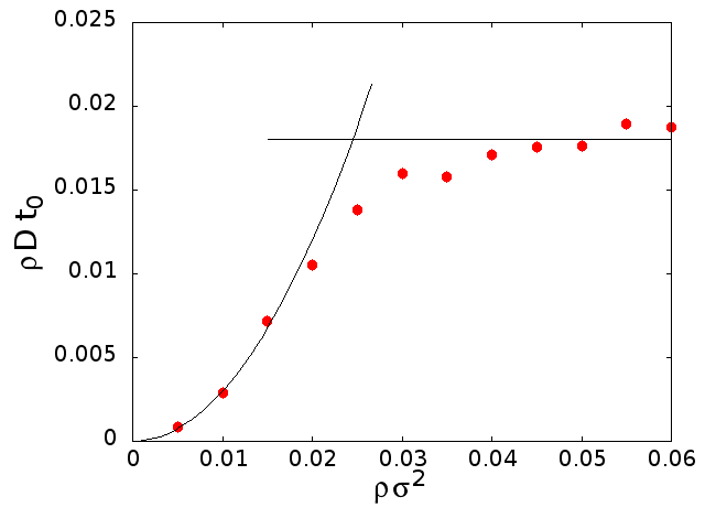
Here is the unit of energy, and ( is the length unit, practically corresponding to the disk diameter). The disks move in a 2D square box of side , where is the density of the disks. Periodic boundary conditions have been used. The unit of time is where is the mass of the disks. The free particle diffusivity is . After thermalization, at a temperature , we extract the diffusion coefficient of the interacting disks. Due to the Einstein relation, the diffusivity is inversely proportional to the viscosity . Here is the thickness of the weak link layer. In Fig. 9 we plot the product as a function of . We find a low density regime in which the long range Gaussian interaction is dominant and the diffusion coefficient increases with the density. At higher densities, on the other hand, the short range repulsion becomes dominant, and the diffusion coefficient decreases roughly linearly with the density, giving rise to a constant product .
To mimic the vortex dynamics, we assume that of the disks is proportional to . Here the coherence length plays the role of the radius of the vortex core. The corresponding horizontal scale in the plot of Fig. 9 shows that the crossover occurs at Oe if the vortex core m. This points to quite extended Pearl vortices which are of no surprise in our structure. Next, we trade for in the Einstein relation so that :
| (7) |
where and Eq. (4) has been used in the last equality to connect the viscosity to the flux flow resistivity .
References
- [1] Y.-J. Doh, J. A. van Dam, A. L. Roest, E. P. A. M. Bakkers, L. P. Kouwenhoven, and S. De Franceschi, Science 309, 272 (2005).
- [2] A. H. Castro Neto, F. Guinea, N. M. R. Peres, K. S. Novoselov, and A. K. Geim, Rev. Mod. Phys. 81, 109 (2009).
- [3] C. W. J. Beenakker, Rev. Mod. Phys. 80, 1337 (2008).
- [4] X.-L. Qi and S.-C. Zhang, Rev. Mod. Phys. 83, 1057 (2011).
- [5] M. Z. Hasan and C. L. Kane, Rev. Mod. Phys. 82, 3045 (2010).
- [6] F. S. Bergeret, A. F. Volkov, and K. B. Efetov, Rev. Mod. Phys. 77, 1321 (2005).
- [7] A. I. Buzdin, Rev. Mod. Phys. 77, 935 (2005).
- [8] M. Veldhorst, M. Snelder, M. Hoek, T. Gang, V. K. Guduru, X. L. Wang, U. Zeitler, W. G. van der Wiel, A. A. Golubov, H. Hilgenkamp, and A. Brinkman, Nat Mater 11, 417 (2012).
- [9] C. Kurter, A. D. K. Finck, P. Ghaemi, Y. S. Hor, and D. J. Van Harlingen, Phys. Rev. B 90, 014501 (2014).
- [10] L. Galletti, S. Charpentier, M. Iavarone, P. Lucignano, D. Massarotti, R. Arpaia, Y. Suzuki, K. Kadowaki, T. Bauch, A. Tagliacozzo, F. Tafuri, and F. Lombardi, Phys. Rev. B 89, 134512 (2014).
- [11] J. Alicea, Reports on Progress in Physics 75, 076501 (2012).
- [12] C. Beenakker, Annual Review of Condensed Matter Physics 4, 113 (2013).
- [13] V. L. Berezinskiǐ, Soviet Journal of Experimental and Theoretical Physics 34, 610 (1972).
- [14] J. M. Kosterlitz and D. J. Thouless, Journal of Physics C Solid State Physics 6, 1181 (1973).
- [15] B. Jouault, S. Charpentier, D. Massarotti, A. Michon, M. Paillet, J.-R. Huntzinger, A. Tiberj, A. Zahab, T. Bauch, P. Lucignano, A. Tagliacozzo, F. Lombardi, and F. Tafuri, J. Supercond. Nov. Magn. 29, 1145 (2016).
- [16] J. Kedzierski, P.-L. Hsu, P. Healey, P. Wyatt, C. Keast, M. Sprinkle, C. Berger, and W. A. de Heer, IEEE Transactions on Electron. Devices 55, 2078 (2008).
- [17] C. W. J. Beenakker, Phys. Rev. Lett. 97, 067007 (2006).
- [18] M. Titov, A. Ossipov, and C. W. J. Beenakker, Phys. Rev. B 75, 045417 (2007).
- [19] A. M. Black-Schaffer and S. Doniach, Phys. Rev. B 78, 024504 (2008).
- [20] T. Dirks, T. L. Hughes, S. Lal, B. Uchoa, Y. F. Chen, C. Chialvo, P. M. Goldbart, and N. Mason, Nature Physics 7, 386 (2011).
- [21] M. Ben Shalom, M. J. Zhu, V. I. Fal’ko, A. Mishchenko, A. V. Kretinin, K. S. Novoselov, C. R. Woods, K. Watanabe, T. Taniguchi, A. K. Geim, and J. R. Prance, ArXiv e-prints (2015), arXiv:1504.03286 [cond-mat.mes-hall].
- [22] N. Mizuno, B. Nielsen, and X. Du, Nature Communications 4, 2716 (2013).
- [23] V. E. Calado, S. Goswami, G. Nanda, M. Diez, A. R. Akhmerov, K. Watanabe, T. Taniguchi, T. M. Klapwijk, and L. M. K. Vandersypen, Nature nanotechnology 10, 761 (2015).
- [24] C. P. Bean, Physical Review Letters 8, 250 (1962).
- [25] B. M. Kessler, C. O. Girit, A. Zettl, and V. Bouchiat, Phys. Rev. Lett. 104, 047001 (2010).
- [26] P. A. Rosenthal, M. R. Beasley, K. Char, M. S. Colclough, and G. Zaharchuk, Appl. Phys. Lett. 59, 3482 (1991).
- [27] A. Michon, S. Vézian, A. Ouerghi, M. Zielinski, T. Chassagne, and M. Portail, Appl. Phys. Lett. 97, 171909 (2010).
- [28] B. Jabakhanji, A. Michon, C. Consejo, W. Desrat, M. Portail, A. Tiberj, M. Paillet, A. Zahab, F. Cheynis, F. Lafont, F. Schopfer, W. Poirier, F. Bertran, P. Le Fèvre, A. Taleb-Ibrahimi, D. Kazazis, W. Escoffier, B. C. Camargo, Y. Kopelevich, J. Camassel, and B. Jouault, Phys. Rev. B 89, 085422 (2014).
- [29] G. Giovannetti, P. A. Khomyakov, G. Brocks, V. M. Karpan, J. van den Brink, and P. J. Kelly, Phys. Rev. Lett. 101, 026803 (2008).
- [30] L. Longobardi, D. Massarotti, G. Rotoli, D. Stornaiuolo, G. Papari, A. Kawakami, G. P. Pepe, A. Barone, and F. Tafuri, Phys. Rev. B 84, 184504 (2011).
- [31] D. Stornaiuolo, G. Rotoli, D. Massarotti, F. Carillo, L. Longobardi, F. Beltram, and F. Tafuri, Phys. Rev. B 87, 134517 (2013).
- [32] A. Barone and G. Paternò, Physics and applications of the Josephson effect (Wiley, 1982).
- [33] J. M. Martinis, and R. L. Kautz, Phys. Rev. Lett. 63, 1507-1510 (1989).
- [34] L. G. Aslamasov and A. I. Larkin, Physics Letters A 26, 238 (1968).
- [35] A. T. Fiory, A. F. Hebard, and W. I. Glaberson, Phys. Rev. B 28, 5075 (1983).
- [36] B. Halperin and D. R. Nelson, Journal of Low Temperature Physics 36, 599 (1979).
- [37] I. V. Borzenets, U. C. Coskun, S. J. Jones, and G. Finkelstein, Phys. Rev. Lett. 107, 137005 (2011).
- [38] L. Ji, M. S. Rzchowski, N. Anand, and M. Tinkham, Phys. Rev. B 47, 470 (1993).
- [39] M. Tinkham, Introduction to Superconductivity (McGraw-Hill, Singapore, 1996).
- [40] S. Prestipino, F. Saija, and P. V. Giaquinta, Phys. Rev. Lett. 106, 235701 (2011).
- [41] R. H. Koch, V. Foglietti, W. J. Gallagher, G. Koren, A. Gupta, and M. P. A. Fisher, Phys. Rev. Lett. 63, 1511 (1989).
- [42] A. Palau, T. Puig, X. Obradors, E. Pardo, C. Navau, A. Sanchez, A. Usoskin, H. C. Freyhardt, L. Fernández, B. Holzapfel, and R. Feenstra, Applied Physics Letters 84, 230 (2004).
- [43] A. Palau, T. Puig, X. Obradors, and C. Jooss, Phys. Rev. B 75, 054517 (2007).
- [44] E. Zeldov, J. R. Clem, M. McElfresh, and M. Darwin, Phys. Rev. B 49, 9802 (1994).
- [45] C. P. Bean and J. D. Livingston, Phys. Rev. Lett. 12, 14 (1964).
- [46] P. G. De Gennes, Superconductivity of Metals and Alloys, Advanced book classics (Perseus, Cambridge, MA, 1999).
- [47] V. N. Kopylov, A. E. Koshelev, I. F. Schegolev, and T. G. Togonidze, Physica C 170, 291 (1990).
- [48] S. Hart, H. Ren, T. Wagner, P. Leubner, M. Mühlbauer, C. Brüne, H. Buhmann, L. W. Molenkamp, and A. Yacoby, Nature Physics 10, 638 (2014).
- [49] J. Yong, T. R. Lemberger, L. Benfatto, K. Ilin, and M. Siegel, Phys. Rev. B 87, 184505 (2013).
- [50] A. Y. Aladyshkin, A. V. Silhanek, W. Gillijns, and V. V. Moshchalkov, Superconductor Science Technology 22, 053001 (2009), arXiv:0902.1630 [cond-mat.supr-con].