Interlayer Transport through a Graphene / Rotated-Boron-Nitride / Graphene Heterostructure
Abstract
Interlayer electron transport through a graphene / hexagonal boron-nitride (h-BN) / graphene heterostructure is strongly affected by the misorientation angle of the h-BN with respect to the graphene layers with different physical mechanisms governing the transport in different regimes of angle, Fermi level, and bias. The different mechanisms and their resulting signatures in resistance and current are analyzed using two different models, a tight-binding, non-equilibrium Green function model and an effective continuum model, and the qualitative features resulting from the two different models compare well. In the large-angle regime (), the change in the effective h-BN bandgap seen by an electron at the point of the graphene causes the resistance to monotonically increase with angle by several orders of magnitude reaching a maximum at . It does not affect the peak-to-valley current ratios in devices that exhibit negative differential resistance. In the small-angle regime (), Umklapp processes open up new conductance channels that manifest themselves as non-monotonic features in a plot of resistance versus Fermi level that can serve as experimental signatures of this effect. For small angles and high bias, the Umklapp processes give rise to two new current peaks on either side of the direct tunneling peak.
I Introduction
Graphene (Gr), a two-dimensional (2D) material made of carbon atoms arranged in a honeycomb structure, has excellent electronic, thermal, and mechanical properties that make it a promising candidate for nanoelectronic devices[1, 2]. 2D hexagonal boron nitride (h-BN) has the same 2D honeycomb structure as graphene. Its lattice constant is closely matched to that of graphene, and its large band gap and good thermal and chemical stability make it an excellent insulator, substrate, and encapsulating material for graphene and other 2D materials.[3, 4] There have been a number of experimental and theoretical studies of the in-plane electronic properties of graphene on h-BN.[5, 6, 7, 8, 9, 10] In general, in a h-BN graphene heterolayer system, whether grown by chemical vapor deposition or assembled by mechanical stacking, the graphene will not be crystallographically aligned with the h-BN. The misalignment results in a small change in the in-plane graphene electron velocity [8].
Interest in the effect of misorientation on cross-plane transport began with bilayer graphene, and the first coherent tunneling calculations showed a 16 order of magnitude change in the interlayer resistance as a function of the misalignment angle.[11] Including phonon mediated transport reduced the dependence on angle to a few orders of magnitude.[12] Replacing the source and drain misoriented graphene sheets with source and drain misoriented graphite leads resulted in the same angular dependence and very similar quantitative values for the coherent current.[13] This demonstrated sensitivity to interlayer misorientation motivates us to examine the effect in Gr/BN/Gr devices.
There is also significant interest in Gr/BN/Gr heterostructures for electronic device applications [14, 15, 16, 17, 18, 19, 20, 21, 22, 23, 24, 25, 26, 27, 28, 29, 30, 31, 32, 33]. Gr/BN/Gr structures display negative differential resistance (NDR),[20, 34, 24, 30, 31, 32, 27] and theoretical calculations predict maximum frequencies of several hundred GHz.[26] The NDR arises from the line-up of the source and drain graphene Dirac cones combined with the conservation of in-plane momentum. In one experiment in which plateaus were observed in the current-voltage characteristics instead of NDR, the experimental results could be matched theoretically by ignoring momentum conservation.[23] In the theoretical treatments, the focus has been primarily on the rotation between top and bottom graphene layers and the resulting misalignment of the Dirac cones [20, 27, 32]. Recently, the effect of misalignment of both the BN and the graphene layers including the effects of phonon scattering have been investigated using the low-angle effective continuum model [35, 30].

In this work, we focus on the effect of the BN misalignment and consider a system of two aligned graphene layers serving as the source and the drain separated by one or more AB stacked layers of h-BN that are misoriented with respect to the graphene. An illustration of such a system is shown in Fig. 1(a). This system is analyzed using two different models and the results from the two models are compared. Commensurate rotation angles in the range are simulated with a tight binding model and the non-equilibrium Green function (NEGF) formalism. The small angle regime is also analyzed with a continuum model similar to that used in Ref. [35]. The qualitative features of the two different models compare well, and the continuum model elucidates the physics of the small angle regime
The misorientation of the BN with respect to the graphene can have several possible effects that dominate in different regimes of angle and applied bias. (a) For devices under high bias, it can alter the transverse momentum conservation and thus degrade the NDR. (b) It can alter the potential barrier seen by the electrons at the K points in the graphene, and thus alter the interlayer tunneling current and resistance. (c) As in misoriented graphene on graphene, it can result in destructive quantum interference that reduces the current. A signature of this effect is that over a range of angles, the coherent interlayer resistance scales monotonically with the size of the commensurate unit cell.[12, 13] (d) For small angle rotations, Umklapp processes can open up new channels of conductance resulting in new features that depend on Fermi level, angle, and bias. The presence or absence of these effects and under what conditions they manifest themselves will become clear in the analysis.
The paper is organized as follows. Sec. II.1, describes the tight binding model and the NEGF method used to calculate the coherent resistance for different commensurate angles and different h-BN layer thicknesses. Sec. II.2 describes the effective continuum model employed to analyze the low angle regime. Sec. III describes and discusses the results. Conclusions are given in Sec. IV. The appendix gives details of the tight-binding model and calculations.
II Models and Methods
II.1 Tight Binding Transport Calculations
The interlayer transport in the Gr/BN/Gr device illustrated in Fig. 1 is analyzed using a tight binding Hamiltonian and a non-equilibrium Green function (NEGF) approach for the transport. The device Hamiltonian has the following block tridiagonal form
| (1) |
where is the wavevector in the plane, is the Hamiltonian of the uncoupled top (bottom) graphene layers, is the Hamiltonian of the h-BN layer(s), and is the block of matrix elements coupling to . The elements of the off-diagonal blocks representing the interaction between atom in a graphene layer and atom in the adjacent h-BN layer are given by [12]
| (2) |
where is the interlayer disatnce, is the distance between two atoms and , and is the projected in-plane distance between the two atoms. The lattice constant of the entire system is set to that of graphene. The misoriented commensurate primitive unit cells are created using the approach described in Ref. [36]. Parameters for this tight binding model were extracted by fitting the band structures to density functional theory (DFT) results. The on-site energy for , is set to and the on-site energies of the and atoms are 3.40 eV and -1.31 eV, respectively. For multiple h-BN layers, we adapt the interlayer h-BN interaction strength from Ref. [37]. All other parameters are shown in Table 1.
| in-plane interaction | Interlayer interaction | |||||
| C-C | 2.85 | 0.39 | 3.35 | 0.60 | 1.70 | 1.65 |
| B-N | 2.52 | 0.60 | ||||
| C-B | 0.62 | 3.22 | 0.54 | 0.84 | 2.04 | |
| C-N | 0.38 | 3.22 | 0.41 | 0.97 | 2.03 | |
Since this is essentially a 2D - 2D tunneling problem, the coherent interlayer transmission through the Gr/BN/Gr structure is calculated within a NEGF approach using the ‘generalized boundary conditions’ described in Ref. [38]. Within the NEGF approach, the graphene layers act as the ‘contacts’ and the h-BN layer acts as the ‘device’. The surface Green’s functions of the top and bottom graphene layers are
| (3) |
where is the identity matrix, and the energy broadening = 80 meV is chosen to match that of Ref. [39]. Given the surface Green’s functions, the rest of the NEGF calculations follow as usual. Here the ‘device’ Green’s function is
| (4) |
where the self energies resulting from coupling to the graphene layers are and . The transmission coefficient is
| (5) |
where , , is the spectral function of the top (bottom) graphene layer, and indicates a trace of the matrix.
Integrating Eq. (5) for the transmission over the first commensurate Brillouin zone, the energy-dependent transmission coefficient per unit area is
| (6) |
This integration is performed numerically on a square grid with (see Appendix A for further details). The linear conductance is given by
| (7) |
where the factor of 2 accounts for the spin degeneracy, and the integration over accounts for the valley degeneracy. The resistance is the inverse of the conductance, .
For finite bias calculations, an applied bias is symmetrically applied across the device by setting and . When multiple BN layers are present, the potential drops linearly within the BN region, since BN is an insulator. The tunneling current flowing through the device is given by:
| (8) |
where and are the chemical potentials of the top and bottom graphene, respectively, is the Fermi distribution function, and is the potential difference between the charge neutral points of the two Gr layers. accounts for the effect of gating and doping. We refer to as the built-in potential in analogy with a pn junction, since this is the potential that exists before the bias is applied.
II.2 Effective Continuum Model
As the rotation angles become smaller the commensurate unit cells become very large. As a result, NEGF calculations with the large tight binding Hamiltonians become computationally challenging. In order to better understand the physics governing the interlayer transport at small rotation angles, we construct an effective continuum model. In the small angle region (), the coupling matrix between graphene and h-BN layer is of the following form [30, 39, 20]
| (9) |
where
| (10) |
In Eq. (10), the row indices correspond to the and atom of the graphene, and the column indices correspond to the and atoms of the BN. The lower off-diagonal element corresponds to a C atom directly over a B atom. All other elements correspond to a C atom in the center of an equilateral triangle of B atoms or N atoms. The hopping amplitudes and between a C atom and a B or N atom are the same as those listed in Table 1. The phase factors result from the matrix elements of the Bloch sums evaluated at the points. The momentum shift is the misalignment between the point of h-BN and graphene. Specifically,
| (11) |
where is the magnitude of the point of graphene. When , , and the sum in Eq. (9) will cause the diagonal and upper off-diagonal elements of to vanish leaving a coupling matrix corresponding to AB stacking with the B atom directly above the C atom.
By eliminating from Hamiltonian (1), we reduce the Hamiltonian into an effective Hamiltonian and obtain the effective interaction Hamiltonian between the top and bottom graphene layers as [40]
| (12) |
The low-energy electronic structure of h-BN can be described by a gapped Dirac-like Hamiltonian that acts on the B and N orbital basis around a given point,
| (13) |
The energies and are the on-site energies of the B and N atoms, while is the velocity that is determined by the in-plane matrix elements between the B and N atoms given in Table 1. Combining Eqs. (9), (12), and (13), the effective interaction Hamiltonian is
| (14) |
where is the momentum difference shift during transmission. Since the top and bottom graphene layers are aligned (),
| (15) |
This can be interpreted as the momentum being conserved for transmission between aligned Dirac cones of the top and bottom graphene layers. For transmission between misaligned Dirac cones, the momentum shifts by .
The tunneling matrix element for the transmission between the top and bottom layers is:
| (16) |
where
| (17) |
and the eigenvectors of the graphene layers are , where is the band index. The linear conductance is [11]
| (18) |
or
| (19) |
where and account for the spin and valley degeneracy, respectively, and is the cross sectional area. is the spectral function. For simplicity we can approximate by a Lorentzian function near the Fermi energy and use a broadening lifetime same as the NEGF calculations[32].
To better understand the effect of the rotation, we divide the conductance into three parts.
| (20) |
where the first part
| (21) |
represents the coherent transport process where the momentum is conserved between top and bottom graphene layers. The second and third terms correspond to Umklapp processes in which the second term is an intraband process
| (22) |
and the third term is an interband process,
| (23) |
III Results
Fig. 2 shows the tight-binding, NEGF calculations of the zero-temperature, coherent resistance versus Fermi energy () for heterostructures with (a) a single h-BN layer and (b) 3 h-BN layers. The Fermi level, , varies from -0.5 eV to 0.5 eV around the charge neutrality point for a range of rotation angles from to as indicated in the legend. The lowest black curve is the coherent resistance for the ABA unrotated heterostructure. For all of the angles shown, the resistance monotonically falls as the Fermi level moves away from the charge neutrality point where the density of states of the graphene layers are a minimum. In contrast to rotated bilayer graphene (r-BLG), for the two lowest angles, and , there is no sudden change in resistance with Fermi energy around 0.3-0.4 eV (compare with Fig. 2(a-b) of Ref. [13]).
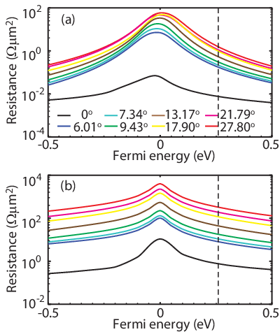
The vertical dashed lines in Fig. 2 correspond to a Fermi level of 0.26 eV. This is the Fermi level previously used for comparisons of the interlayer conductivity of misoriented bilayer graphene [11, 12, 13]. The numerical values of the resistance at eV are given in Table 2. As the h-BN layer becomes misaligned, the resistances increase by factors of 200 and 430 for the monolayer and trilayer BN structures, respectively. This trend in the variation of resistance with rotation angle is similar to the experimental observations in Ref. [14]. There it was shown that the conductance can vary by a factor of 100 for different devices with the same h-BN thickness. For both the monolayer and trilayer BN structures, the increase in the resistance is a monotonic function of the BN rotation angle as the rotation angle increases from to . This trend is also in contrast to that of r-BLG. In the r-BLG system, at low energies near the charge neutrality point, the coherent interlayer resistance is a monotonic function of the supercell lattice constant as opposed to the rotation angle (compare to Fig. 1(d) of Ref. [12]).
| Rotation angle (degrees) | Energy gap (eV) | Coherent Resistance () | |
| Gr/1L h-BN/Gr | Gr/3L h-BN/Gr | ||
| 0.00 | 4.709 | 0.007601 | 0.7972 |
| 1.25 | 4.726 | 0.03710 | |
| 1.41 | 4.730 | 0.03758 | |
| 1.54 | 4.734 | 0.03711 | |
| 1.61 | 4.737 | 0.03521 | |
| 1.70 | 4.740 | 0.03308 | |
| 1.79 | 4.743 | 0.03028 | |
| 1.89 | 4.748 | 0.02844 | 2.752 |
| 2.00 | 4.752 | 0.02954 | |
| 2.13 | 4.758 | 0.03481 | |
| 2.45 | 4.774 | 0.05355 | |
| 2.88 | 4.798 | 0.07565 | 4.474 |
| 3.15 | 4.815 | 0.08741 | |
| 3.48 | 4.838 | 0.09981 | |
| 3.89 | 4.869 | 0.1132 | 5.510 |
| 4.41 | 4.913 | 0.1288 | 6.094 |
| 5.08 | 4.976 | 0.1481 | 6.977 |
| 6.01 | 5.075 | 0.1753 | 8.495 |
| 7.34 | 5.237 | 0.2182 | 11.43 |
| 9.43 | 5.529 | 0.3048 | 18.87 |
| 13.17 | 6.106 | 0.5371 | 46.48 |
| 17.90 | 6.813 | 0.9770 | 123.6 |
| 21.79 | 7.280 | 1.120 | 199.7 |
| 27.80 | 7.686 | 1.563 | 344.3 |
To investigate process (b) in which rotation of the BN alters the tunnel barrier, we calculate the energy gap of ML and trilayer h-BN at the BN -point corresponding to graphene’s -point as a function of rotation angle as illustrated in Fig. 1(b). The resulting effective bandgap for ML BN is plotted versus rotation angle in Fig. 1(c). Since the direct bandgap (4.7 eV) of h-BN occurs at its -point, the minimum BN bandgap ‘seen’ by an electron at the -point in the graphene layer occurs for BN rotation angles of and when graphene’s point is aligned with BN’s or points. The effective BN bandgap seen by an electron at the -point in the graphene layer monotonically increases as the BN is rotated from , and it reaches a maximum at . In the Brillouin zone of the BN, this corresponds to the bandgap near the point. This monotonic increase in the tunnel barrier with angle follows the same monotonic trend as the increase in resistance with angle.
To analyze the relation between the effective energy gap and resistance, we show in Fig. 3 a semi-log plot of the resistance as a function of the effective BN band gap (for different rotation angles) at 0.26 eV. For angles greater than , the tunnel current scales exponentially with the effective bandgap as one would expect for tunneling through a potential barrier. Therefore, for , we find that the dominant process affecting the tunnel current is the change in the effective BN bandgap ‘seen’ by the electrons at the point in graphene.

However, for small angles , there is clearly a very different trend and a different dependence of the resistance on the BN rotation angle. The different dependencies arise from different parallel conductance channels that dominate at different angle regimes. To analyze the low-angle region of the curve, we turn to the effective continuum model.
A more detailed picture of the low-angle regime is given in Fig. 4 which shows the resistance versus BN rotation angle calculated with both the continuum model and the NEGF tight-binding model for two values of . The solid lines are from the continuum model, and the triangles are from the NEGF, tight-binding model. More low-angles are included in the NEGF calculations, and the smallest rotated angle calculated from the NEGF, tight-binding model is . Both models show a non-monotonic dependence of resistance on angle at very low angles . While the magnitudes differ between the two models, the overall trends match well.
The continuum model tells us that there are three parallel conductance channels corresponding to the direct and two Umklapp processes in Eqs. (20) - (23). The individual channels dominate in different angle regimes. The angle at which each channel dominates is primarily determined by the overlap of the spectral functions in Eqs. (21) - (23). For the direct term, of Eq. (21), the spectral functions always overlap since the top and bottom graphene layers are aligned. For the two Umklapp terms, the overlaps of the spectral functions are functions of the angles, and the overlaps become negligible for . Therefore, for larger angles, , the direct channel dominates, and the dependence on the angle is through the matrix element which, through and the effective interaction, includes the effect of the increase in the apparent BN bandgap with angle as described above and shown in Fig. 1(c).
The maximum overlap of the spectral functions in the ‘interband’ term of Eq. (23) occurs when . This term is maximum at rotation angle , and it decreases for angles greater than or less than . This interband term is responsible for the dip in resistance for between one to two degrees in Fig. 4. It also explains the shift in angle with Fermi level. As the Fermi level is increased, the local minimum moves to larger rotation angles since the angle of maximum overlap is linearly proportional to .
The maximum overlap of the spectral functions in the ‘intraband’ term of Eq. (22) occurs at . As increases, this channel monotonically decreases with the decrease governed by the decreasing overlap of the spectral functions. Since this channel has a maximum as goes to zero, it governs the initial increase in resistance for the smallest angles.

The three individual contributions to the continuum model, direct, interband, and intraband, are shown in Fig. 5 for the two different Fermi levels, 0.26 eV and 0.16 eV.

While analyzing the resistance as a function of rotation angle is useful for clarifying the physics, verifying the trends shown in Fig. 4 would be very difficult experimentally. Experimentally, it is far easier to fix the angle and sweep the Fermi level of the top and bottom graphene layers. The resulting resistances calculated both from the NEGF, tight-binding and the continuum models for a 1-ML BN rotation angle of are shown in Fig. 6(a).

Both models show non-monotonic behavior of the resistance as the Fermi level is swept between 0.5 and 0.6 eV. To observe this feature at lower Fermi levels, a smaller angle is required, and to observe the feature experimentally a larger resistance is required. The larger resistance is achieved by increasing the number of BN layers from 1 to 5. The resistance versus Fermi level calculated from the continuum model for a 5-ML BN layer rotated by is shown in Fig. 6(b). The non-monotonic feature moves to lower energies and now occurs as the Fermi level is swept between 0.2 and 0.3 eV. The overall magnitude of the resistance is between 100 and 1000 which should be large enough to be ovservable, and it can be increased by increasing the number of BN layers.
So far, we have focused on the 0-bias resistivity to elucidate the physics. However, interest in this system is driven by potential applications, and one application of current investigation is a high-frequency oscillator that exploits the negative differential resistance observed under high-bias. To understand how the misorientation of the BN layer affects the current-voltage (I-V) characteristic of this structure, we show in Fig. 7 the NEGF, tight-binding calculations using Eq. (8) of the I-V characteristics for the unrotated structure and the structure with the BN layer rotated by for BN layer thicknesses of 1 ML, 3 ML, and 5 ML. The three I-V characteristics in each plot are for three different built-in potentials between the two graphene layers. The panels on the left are for the unrotated structure while the panels on the right are for the structure. In Fig. 7(a) and (b), it is shown that the rotation of monolayer h-BN decreases the current by nearly 2 orders of magnitude. This relative decrease in the tunneling current becomes progressively greater as the number of h-BN layers is increased, as shown in the other subplots. For the case of 5 h-BN layers, the tunneling current is nearly 4 orders of magnitude smaller. As expected, this decrease in the tunneling current and its scaling is consistent with the resistance increasing with the rotation angles as shown in Fig. 2. While the current decreases with rotation angle, the peak-to-valley current ratio is unaffected. For high-frequency applications, both high current density and high peak-to-valley ratios are desirable, and rotation of the BN layer provides one more tool for engineering optimal electronic properties for applications.
For small rotation angles, it is interesting to consider whether new qualitative features appear in the nonlinear I-V characteristic. To answer that question, we applied the effective continuum model to calculate I-V curves of a structure with . The results in Fig. 8, for 3 different values of built-in voltage , are qualitatively different from the I-V curves for large angle rotation, since several regions of NDR appear depending on the initial built-in potential. The first and third peaks arise from the interband component which is maximum at . The middle peak that occurs at is caused by the direct tunneling term.


IV Conclusions
Electron transport through a Gr / h-BN / Gr structure is examined within a tight-binding model with commensurate rotation angles and within an effective continuum model. The two graphene layers are aligned, and the h-BN layer is rotated by an angle with respect to the graphene layers. For angles greater than , the resistance is dominated by the change in the effective h-BN bandgap seen by an electron at the point of the graphene. In this large-angle regime, the effect of rotating the BN is to increase the barrier height of the BN tunnel barrier at the point of the graphene. For , the resistance monotically increases with the rotation angle, and it reaches a maximum at . As is increased from to , the coherent interlayer resistance increases by factors of 200 and 430 for monolayer and trilayer BN layers, respectively. For devices that exhibit NDR under high bias, rotation of the h-BN primarily serves to reduce the overall magnitude of the current. It does not degrade the peak to valley current ratios. In this large-angle regime, since the dominant physics is that of single-barrier direct tunneling, phonon-scattering should have negligible effect on the low-bias, angle-dependent trends and magnitudes of the interlayer resistances. Since NDR results from momentum conservation, phonon-scattering will reduce the peak-to-valley ratios, but this effect also exists in the unrotated structure. While we do not expect a significant dependence of the phonon scattering on the rotation angle of the h-BN in the large-angle regime, this is an open question for further study.
The small-angle regime () reveals qualitatively new features both in the low-bias
interlayer resistances and in the high-bias I-V characteristics.
The new features arise due to the opening of new conductance channels corresponding to
Umklapp processes.
With the two graphene layers aligned, Umklapp processes give rise to two new
conduction channels corresponding to an intraband term and an interband term.
The angular and energy dependence of these terms is primarily determined
by the overlap of the top and bottom graphene spectral functions that are shifted in momentum space
with respect to each other by an Umklapp lattice vector.
For a fixed rotation angle of the h-BN layer, both the intraband
and interband terms peak at a Fermi level
.
At this Fermi level, the two spectral functions in the interband term perfectly
overlap, so that the interband term dominates.
This strong peak in the interband term results in a distinct, non-monotonic feature
in a plot of the interlayer resistance versus Fermi energy that occurs
as the Fermi level is swept through .
The qualitative trends of this non-monotonic feature are
reproduced in the tight-binding calculations for structures with small
commensurate rotation angles, although the overall magnitude of the
feature is less.
The interband term also gives rise to two extra peaks in the nonlinear characteristic
on either side of the peak resulting from the direct tunneling term.
Amorim et al. [35] found that
phonon scattering and incoherent scattering in this low-angle regime reduces the magnitude
of the features resulting from Umklapp processes, but it does not remove them, so that the
new features in the low-angle regime should be experimentally observable.
Acknowledgement: This work is supported in part by FAME, one of six centers of STARnet, a Semiconductor Research Corporation program sponsored by MARCO and DARPA and the NSF EFRI-143395. This work used the Extreme Science and Engineering Discovery Environment (XSEDE), which is supported by National Science Foundation grant number ACI-1053575.
Appendix A Tight-binding model and method details
The transmission coefficient over in the first Brillouin zone, was numerically integrated on a square grid with . Fig. 9 shows the momentum resolved transmission in the first Brillouin zone corresponding to the two commensurate rotation angles of and at eV. The transmission is centered at the K and K’ and peaks on the isoenergy surface.

To extract a tunneling decay constant of the BN predicted by the interlayer tight-binding parameters, we calculate the resistance of 1, 3, 5, and 7 layers of h-BN for two angles of and at eV. Fig. 10 shows the exponential increase in resistance with increasing number of h-BN layers for both structures. Fitting the results to an exponential function, , where is the number of h-BN layers gives values for of 2.6 and 3.6 for the unrotated and rotated structures, respectively. These values are similar to an experimentally extracted value of [41].

References
- [1] K. S. Novoselov, V. Fal, L. Colombo, P. Gellert, M. Schwab, and K. Kim, Nature 490, 192 (2012).
- [2] A. H. Castro Neto, F. Guinea, N. M. R. Peres, K. S. Novoselov, and A. K. Geim, Rev. Mod. Phys. 81, 109 (2009).
- [3] C. R. Dean, A. F. Young, I. Meric, C. Lee, L. Wang, S. Sorgenfrei, K. Watanabe, T. Taniguchi, P. Kim, and K. Shepard, Nature nanotechnology 5, 722 (2010).
- [4] J. Xue, J. Sanchez-Yamagishi, D. Bulmash, P. Jacquod, A. Deshpande, K. Watanabe, T. Taniguchi, P. Jarillo-Herrero, and B. J. LeRoy, Nature Materials 10, 282 (2011).
- [5] C. Hwang, D. A. Siegel, S.-K. Mo, W. Regan, A. Ismach, Y. Zhang, A. Zettl, and A. Lanzara, Scientific Reports 2 (2012), 10.1038/srep00590.
- [6] B. Hunt, J. D. Sanchez-Yamagishi, A. F. Young, M. Yankowitz, B. J. LeRoy, K. Watanabe, T. Taniguchi, P. Moon, M. Koshino, P. Jarillo-Herrero, and R. C. Ashoori, Science 340, 1427 (2013).
- [7] J. C. W. Song, A. V. Shytov, and L. S. Levitov, Phys. Rev. Lett. 111, 266801 (2013).
- [8] X. Zhao, L. Li, and M. Zhao, Journal of Physics: Condensed Matter 26, 095002 (2014).
- [9] C. R. Woods, L. Britnell, A. Eckmann, R. S. Ma, J. C. Lu, H. M. Guo, X. Lin, G. L. Yu, Y. Cao, R. V. Gorbachev, A. V. Kretinin, J. Park, L. A. Ponomarenko, M. I. Katsnelson, Y. N. Gornostyrev, K. Watanabe, T. Taniguchi, C. Casiraghi, H.-J. Gao, A. K. Geim, and K. S. Novoselov, Nature Physics 10, 451 (2014).
- [10] J. Jung, A. DaSilva, A. H. MacDonald, and S. Adam, Nature Communications 6, 6308 (2014), 1403.0496 .
- [11] R. Bistritzer and H. MacDonald A., Phys. Rev. B 81, 245412 (2010).
- [12] V. Perebeinos, J. Tersoff, and P. Avouris, Phys. Rev. Lett. 109, 236604 (2012).
- [13] K. M. M. Habib, S. S. Sylvia, S. Ge, M. Neupane, and R. K. Lake, Applied Physics Letters 103, 243114 (2013), 10.1063/1.4841415.
- [14] L. Britnell, R. V. Gorbachev, R. Jalil, B. D. Belle, F. Schedin, A. Mishchenko, T. Georgiou, M. I. Katsnelson, L. Eaves, S. V. Morozov, N. M. R. Peres, J. Leist, A. K. Geim, K. S. Novoselov, and L. A. Ponomarenko, Science 335, 947 (2012a).
- [15] T. Georgiou, R. Jalil, B. D. Belle, L. Britnell, R. V. Gorbachev, S. V. Morozov, Y.-J. Kim, A. Gholinia, S. J. Haigh, O. Makarovsky, L. Eaves, L. A. Ponomarenko, A. K. Geim, K. S. Novoselov, and A. Mishcheno, Nature Nanotechnology 8, 100 (2012).
- [16] R. M. Feenstra, D. Jena, and G. Gu, Journal of Applied Physics 111, 043711 (2012).
- [17] L. Britnell, R. V. Gorbachev, A. K. Geim, L. A. Ponomarenko, A. Mishchenko, M. T. Greenaway, T. M. Fromhold, K. S. Novoselov, and L. Eaves, Nature Communications 4, 1794 (2013).
- [18] L. A. Ponomarenko, B. D. Belle, R. Jalil, L. Britnell, R. V. Gorbachev, A. K. Geim, K. S. Novoselov, A. H. Castro Neto, L. Eaves, and M. I. Katsnelson, Journal of Applied Physics 113, 136502 (2013), http://dx.doi.org/10.1063/1.4795542.
- [19] P. Zhao, R. M. Feenstra, G. Gu, and D. Jena, IEEE Trans. Elect. Dev. PP, 1 (2013).
- [20] A. Mishchenko, J. S. Tu, Y. Cao, R. V. Gorbachev, J. R. Wallbank, M. T. Greenaway, V. E. Morozov, S. V. Morozov, M. J. Zhu, S. L. Wong, F. Withers, C. R. Woods, Y. Kim, K. Watanabe, T. Taniguchi, E. E. Vdovin, O. Makarovsky, T. M. Fromhold, V. I. Fal’ko, A. K. Geim, L. Eaves, and K. S. Novoselov, Nature Nanotechnology 9 (2014), 10.1038/nnano.2014.187.
- [21] M. T. Greenaway, E. E. Vdovin, A. Mishchenko, O. Makarovsky, A. Patane, J. R. Wallbank, Y. Cao, A. V. Kretinin, M. J. Zhu, S. V. Morozov, V. I. Fal[rsquor]ko, K. S. Novoselov, A. K. Geim, T. M. Fromhold, and L. Eaves, Nat Phys 11, 1057 (2015), 1509.06208 .
- [22] F. T. Vasko, Phys. Rev. B 87, 075424 (2013).
- [23] T. Roy, L. Liu, S. de la Barrera, B. Chakrabarti, Z. R. Hesabi, C. A. Joiner, R. M. Feenstra, G. Gu, and E. M. Vogel, Applied Physics Letters 104, 123506 (2014), http://dx.doi.org/10.1063/1.4870073.
- [24] B. Fallahazad, K. Lee, S. Kang, J. Xue, S. Larentis, C. Corbet, K. Kim, H. C. P. Movva, T. Taniguchi, K. Watanabe, L. F. Register, S. K. Banerjee, and E. Tutuc, Nano Letters 15, 428 (2015).
- [25] Y. Zhao, Z. Wan, X. Xu, S. R. Patil, U. Hetmaniuk, and M. P. Anantram, Scientific Reports 5, 10712 (2015).
- [26] J. Gaskell, L. Eaves, K. S. Novoselov, A. Mishchenko, A. K. Geim, T. M. Fromhold, and M. T. Greenaway, Applied Physics Letters 107 (2015), http://dx.doi.org/10.1063/1.4930230.
- [27] T. L. M. Lane, J. R. Wallbank, and V. I. Fal'ko, Applied Physics Letters 107 (2015), http://dx.doi.org/10.1063/1.4935988.
- [28] S. C. de la Barrera and R. M. Feenstra, Applied Physics Letters 106, 093115 (2015), http://dx.doi.org/10.1063/1.4914324.
- [29] S. C. de la Barrera, Q. Gao, and R. M. Feenstra, Journal of Vacuum Science & Technology B 32, 04E101 (2014), http://dx.doi.org/10.1116/1.4871760.
- [30] L. Brey, Phys. Rev. Applied 2, 014003 (2014).
- [31] E. Vdovin, A. Mishchenko, M. Greenaway, M. Zhu, D. Ghazaryan, A. Misra, Y. Cao, S. Morozov, O. Makarovsky, T. Fromhold, A. Patanè, G. Slotman, M. Katsnelson, A. Geim, K. Novoselov, and L. Eaves, Physical Review Letters 116, 186603 (2016).
- [32] K. A. Guerrero-Becerra, A. Tomadin, and M. Polini, Phys. Rev. B 93, 125417 (2016).
- [33] S. B. Kumar, G. Seol, and J. Guo, Applied Physics Letters 101, 033503 (2012).
- [34] S. Hwan Lee, M. Sup Choi, J. Lee, C. Ho Ra, X. Liu, E. Hwang, J. Hee Choi, J. Zhong, W. Chen, and W. Jong Yoo, Applied Physics Letters 104, 053103 (2014), http://dx.doi.org/10.1063/1.4863840.
- [35] B. Amorim, R. M. Ribeiro, and N. M. R. Peres, Phys. Rev. B 93, 235403 (2016).
- [36] S. Shallcross, S. Sharma, E. Kandelaki, and A. Pankratov O., Phys. Rev. B 81, 165105 (2010).
- [37] R. M. Ribeiro and N. M. R. Peres, Phys. Rev. B 83, 235312 (2011).
- [38] G. Klimeck, R. Lake, R. C. Bowen, W. R. Frensley, and T. Moise, Appl. Phys. Lett. 67, 2539 (1995).
- [39] R. Bistritzer and M. A. H, Proceedings of the National Academy of Sciences 108, 12233 (2011).
- [40] M. Kindermann, B. Uchoa, and D. L. Miller, Phys. Rev. B 86, 115415 (2012).
- [41] L. Britnell, R. V. Gorbachev, R. Jalil, B. D. Belle, F. Schedin, M. I. Katsnelson, L. Eaves, S. V. Morozov, A. S. Mayorov, N. M. R. Peres, A. H. C. Neto, J. Leist, A. K. Geim, L. A. Ponomarenko, and K. S. Novoselov, Nano Letters 12, 1707 (2012b), pMID: 22380756, http://dx.doi.org/10.1021/nl3002205 .