ICE-based Custom Full-Mesh Network for the CHIME High Bandwidth Radio Astronomy Correlator
Abstract
New generation radio interferometers encode signals from thousands of antenna feeds across large bandwidth. Channelizing and correlating this data requires networking capabilities that can handle unprecedented data rates with reasonable cost. The Canadian Hydrogen Intensity Mapping Experiment (CHIME) correlator processes 8-bits from digitizer inputs across 400 MHz of bandwidth. Measured in bandwidth, it is the largest radio correlator that has been built. Its digital back-end must exchange and reorganize the 6.6 terabit/s produced by its 128 digitizing and channelizing nodes, and feed it to the 256-node spatial correlator in a way that each node obtains data from all digitizer inputs but across a small fraction of the bandwidth (i.e. ‘corner-turn’). In order to maximize performance and reliability of the corner-turn system while minimizing cost, a custom networking solution has been implemented. The system makes use of Field Programmable Gate Array (FPGA) transceivers to implement direct, passive, full-mesh, high speed serial connections between sixteen circuit boards in a crate, to exchange data between crates, and to offload the data to a cluster of 256 graphics processing unit (GPU) nodes using standard 10 Gbit/s Ethernet links. The GPU nodes complete the corner-turn by combining data from all crates and then computing visibilities. Eye diagrams and frame error counters confirm error-free operation of the corner-turn network in both the currently operating CHIME Pathfinder telescope (a prototype for the full CHIME telescope) and a representative fraction of the full CHIME hardware providing an end-to-end system validation. An analysis of an equivalent corner-turn system built with Ethernet switches instead of custom passive data links is provided.
keywords
Radio astronomy, high speed correlators, field programmable gate arrays, networking§Kevin Bandura
; ; ;
1 Introduction
A new generation of radio telescopes operating or in development, including LOFAR (de Vos et al., 2009), MWA (Lonsdale et al., 2009), LWA (Ellingson et al., 2009), UTMOST (Caleb et al., 2016), CHIME (Bandura et al., 2014), HERA (Pober et al., 2014), HIRAX (Newburgh et al., 2016), and SKA (Carilli & Rawlings, 2004), employ arrays with hundreds or thousands of antenna feeds and large bandwidth, as opposed to more traditional radio interferometers with fewer feeds and large dishes. This moves cost and key challenges of observatory design and construction away from the mechanical structure and cryogenic receivers to digital signal processing, where the information from the feeds is digitized and processed in a radio correlator.
Creating a large, distributed frequency-spatial (FX) correlator system that can process this much data poses a networking challenge (Lutomirski et al., 2011, see e.g.). Indeed, the digitized sky information acquired and channelized by each acquisition node (F-engine) describes the signal content of a few antenna feeds over the whole frequency band. However, each spatial correlation node (X-engine) requires the data from all antenna feeds, but for a subset of the frequency band, so that all inputs can be multiplied together and integrated to form visibilities. This requires an exchange of data that is called the corner-turn, which is akin to a matrix transpose. The corner-turn process implements this transpose, going from a configuration where all the information from one antenna feed across all frequency channels is in one location at the F-engine, to a configuration where all the information from one frequency channel across all antenna feeds is in one location at the X-engine. The total data rate is given by the product of the frequency bandwidth multiplied by the number of inputs
| (1) |
where is the number of digitizer inputs (twice the number of dual polarization antennas), is the operating frequency bandwidth, and is the number of bits per frequency channel. Note that the data-rate is independent of the number of frequency channels that have been produced by the F-engine.
The Canadian Hydrogen Intensity Mapping Experiment (CHIME) instrument is composed of four 20100 m cylindrical reflectors instrumented with 1024 dual polarization feeds. Its FX-architecture correlator processes data from =2048 FPGA-based digitizer inputs across =400 MHz of bandwidth with =8 bits per frequency channel (4 bits real and 4 bits imaginary), resulting in a total of 6.6 Tbit/s of data that needs to be reorganized by a corner-turn system before being fed into 256 GPU-Based correlator nodes that compute the full correlation matrix.
The CHIME GPU X-engine is described in Refs. Denman et al. (2015) and Recnik et al. (2015). A GPU node refers to a networked host with a 10 Gbit/s network card and multiple GPU cards. For CHIME, the nodes have been sized such that the volume of data produced by the FPGA boards may be processed, as well as enabling additional on-site experiments to have real-time data access with some pre-processing. At minimum, each GPU node in the X-engine would process one frequency channel. Through careful software and hardware design each node in this system processes four frequency channels.
The hybrid nature of the correlator system (FPGA based F-engine, GPU based X-engine) was driven by the ability for rapid development and flexibility. The GPU based X-engine enables the flexibility to explore new real-time calibration and expand the capabilities of the system. The hybrid design has already allowed for the addition of a Pulsar back-end to the system, enabling the search and monitoring of pulsar-like objects.
Overall, when CHIME comes online this year, it will be the largest radio correlator that has been built, measured in number of digitizer inputs squared times bandwidth ( multiplies per second). Given the massive amount of data that needs to be moved around, an efficient corner-turn architecture is a cost and complexity driver for the CHIME correlator.
This paper describes the CHIME corner-turn implementation with FPGA-based hardware and firmware. Section 2 describes the corner-turn system architecture, while Section 3 describes the hardware needed to implement it. In Section 4 we describe the testing and performance of the system and Section 5 compares the CHIME corner-turn system with another candidate architecture.
2 Corner-turn System Architecture
The CHIME custom corner-turn network was implemented using the ‘ICE’11 1 ICE is the name of the system, and is not an acronym. electronics framework (Bandura et al., 2016).
The decision to develop custom hardware and firmware instead of using an array of Ethernet switches (an alternative described in Section 5) was based on a combination of cost, performance, technical risks and schedule risks. Since the FPGA required to perform the data acquisition and channelizing provides plenty of multi-gigabit transceivers capable of transmitting data over passive links, and since a backplane was already required to distribute power and timing, interconnecting the ICE motherboards to perform the corner-turn was a matter of adding copper traces and connectors to the backplane–a negligible additional cost for the system. In addition to the performance and risk drivers that pushed the design towards the custom solution, the cost of an array of switches with an instantaneous, non-blocking bandwidth of 6.6 Tbit/s would have been significant in comparison to the total cost of the CHIME F-engine (about $2M including hardware and design engineering).
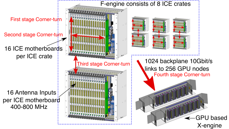
The overall architecture of the CHIME digital back-end is presented in Figure 1. Sky-signals are digitized and channelized at the 2048 inputs of the F-engine which are distributed across 128 custom FPGA-based ICE motherboards (Bandura et al., 2016) housed in eight standard 19” subracks (or crates). Each channelizer partitions the 400 MHz bandwidth data into 1024 frequency channels, each truncated to a complex number consisting of 4 bits real and 4 bits imaginary. The corner-turn system needs to reorder the data such that the 256 GPU correlator nodes each end up with a unique set of frequency channels from every one of the 2048 channelizers.
Overall, the corner-turn operation described above is performed completely by the ICE FPGA-based motherboards and cables in four stages as illustrated in Figures 2 and 3 and described below. All four stages are implemented using a single VHDL module that is configurable for each stage. Note that the bit rates in this section correspond to data rates attributed to the raw data that are being transmitted. Actual line rates are higher, because the packets that are transmitted also include packet headers, error checking cookies, and flagging information. The -2 speed grade Xilinx Kintex 7 series FPGAs used for the ICE system support line rates of 10.2 Gbit/s. Faster speed grades are available that support line rates up to 12.5 Gbit/s.
The first stage is implemented within each FPGA, with no data exchanged between motherboards. Each ICE motherboard processes sixteen analog inputs (51.2 Gbit/s raw data rate). The FPGA receives the 16 inputs and creates 16 new data streams, each of which combines 1/16th of the frequency channels from each of the 16 channelizers.
During the second stage, 15 of these data stream are sent to the other boards within a crate through the backplane mesh network, with one stream remaining local. The end result is that each ICE motherboard in a crate slot gathers data for a specific subset of frequency bins (64 channels total), but from all 256 channelizers in the crate. Approximately 4 Gbit/s of raw data, flags and headers are sent by each backplane link, resulting in about 1 Tbit/s of backplane full-mesh traffic. The packets received through the 15 backplane links are reordered into two streams, with each stream containing half of the received frequency bins.
There are several supported configurations for the third stage, see Section 3.2. For the CHIME implementation, one of the new streams created in stage two is sent to the ICE motherboard at the same slot position in the adjacent crate through four 10 Gbit/s links carried by the backplane Quad Small Form-factor Pluggable Plus (QSFP+) connector. About 7.4 Gbit/s raw data and flags are sent over each of the four links through commercial passive 3 m copper QSFP+ cables. Similarly the other crate provides one of its two streams over the same QSFP+ link. In the end, each ICE motherboard within the pair of crates ends up with a unique subset of 32 frequency bins from 512 channelizers. For CHIME this corresponds to the data from one quarter of the array, or one cylinder. The packets from the local and remote stream are reordered again into eight new streams containing data from 512 analog inputs and four frequency channels.
In the fourth stage, the eight streams from the third stage are provided to eight separate GPU nodes using 10 Gbit/s Ethernet links provided by the two QSFP+ connectors located on the ICE motherboard. Each Ethernet link carries about 7.5 Gbit/s raw data and flag rate. Two active 100 m multi-mode optical fiber QSFP+ cables, each terminated into four independent Small Form-factor Pluggable Plus (SFP+) connectors, are used to carry the data from the ICE motherboards to the GPU nodes, which are located in different buildings. Each SFP+ connector from an ICE motherboard is connected to a different GPU node. A single four-port 10 Gbit/s Ethernet card at each GPU node accommodates the direct links. Overall, a GPU node receives data from a FPGA on an ICE motherboard in each of the four quadrants, and therefore possesses data from four unique frequency bins from all 2048 channelizers.
The final corner-turn step is performed by the host processor on the GPU node (Recnik et al., 2015; Denman et al., 2015; Klages et al., 2015), which recombines the data from its four 10 Gbit/s Ethernet ports to generate four contiguous data blocks containing the data for one frequency bin from every channelizer. These data blocks can then be sent efficiently over the PCI Express bus to the four GPU cores located in the node, where they are correlated.
3 Hardware Implementation


Physically, the corner-turn system is implemented on the same hardware as the F-engine and is distributed across the 128 ICE motherboards that constitute the CHIME correlator F-engine.
Each ICE motherboard hosts two custom full-size FPGA Mezzanine cards (FMC, following the ANSI/VITA 57 standard) which digitize eight analog inputs each. This configuration yields a reasonable board height (9U), a high channel density and requires a number of inputs/outputs (I/O) that is compatible with lower-cost FPGA packages. In addition to its backplane connectivity, each board offers two QSFP+ links that can be used by the FPGA to implement eight bidirectional links at up to 10 Gbit/s each.
Sixteen ICE motherboards are packaged densely into a crate and are connected through a custom backplane which allows for power and timing signal distribution to all boards in the crate. The backplane also provides links between boards located in the same crate and other crates. Figure 4 shows a photo of two interconnected crates, which constitute one quarter of the CHIME’s F-engine and corner-turn system.
The CHIME F-engine and corner-turn system consists of eight crates of ICE motherboards housed in two RF-shielded buildings located below the telescope structure. The data is sent with optical 10 Gbit/s Ethernet links about 100 m away to two separate RF-shielded buildings housing the X-engine GPU nodes.
A global positioning system (GPS) receiver, equipped with an integrated clock distribution module, generates a 10 MHz reference clock and Inter-Range Instrumentation Group B (IRIG-B, Standard 200-04) timestamps that are distributed to each crate via coaxial cable. The backplane distributes these to each of the motherboards. The 10 MHz reference clock is also used to generate all the FPGA clocks and ensures synchronized data acquisition, framing and transmission throughout the array.
The data links provided by the motherboards and backplane are the backbone of the corner-turn system and are described below. Information on the rest of the ICE hardware can be found in Ref. Bandura et al. (2016).
3.1 Full-mesh backplane corner-turn hardware
Stage two of the corner-turn utilizes a full-mesh duplex network that connects every board with every other board in a sixteen-slot ICE crate with a bidirectional link designed to operate at up to 10 Gbit/s in each direction. This network consists of 240 bidirectional high speed serial links embedded in the backplane circuit board. CHIME uses about 40% of the 2.4 Tbit/s theoretical capacity of that network.
Maintaining proper signal integrity of 10 Gbit/s links routed on circuit boards and through connectors requires great care. In order to reduce cross-talk, attenuation and reflections as much as possible, every link consists of differential copper lines implemented as edge-coupled 100 stripline routed on a single layer from the source to the destination point. 25 Gbit/s-rated Molex Impact connectors were used to interface the backplane to the motherboards. Signal reflections are further minimized by back-drilling each of the connector press fit pads. Ground planes separate each of the eight signaling layers required to perform the full mesh. 24 layers were required to complete the backplane routing, with eight signal layers performing the full-mesh.
Circuit board material generally suffers high losses at 10 Gbit/s and had to be chosen carefully to balance cost and performance. Since most of the high speed signal-length occurs over the backplane, it was constructed from Panasonic Megtron 6, a very low-loss hydrocarbon resin material with similar performance to even more expensive hydrocarbon resin materials with ceramic filler (such as Rogers 4350B) that are commonly used for high-frequency, low-loss applications. The maximum attenuation at 5 GHz is expected to be 0.37 dB/inch at 10 Gbit/s, resulting in a maximum backplane attenuation of 6 dB between the furthest slots. The material is expensive, but its cost is justified by the overall signal-integrity advantages and the low number of backplanes in the system.
The motherboards are constructed from a lower-cost 408HR woven glass FR-4 material. The transmission distance link between the FPGA and backplane connector results in an additional 5 dB attenuation.
To further reduce losses, both the backplane and motherboard laminates have been fabricated using very low profile (VLP) copper foil. VLP reduces losses by 0.2 dB/inch for cost increase of only about 2%.
Overall, the worst-case FPGA-to-FPGA attenuation is 16 dB for the longest trace. This is well within the specifications of the Xilinx Kintex 7 GTX transceivers, which can operate at full rate with greater than 20 dB attenuation (Xilinx UG476, 7 Series FPGAs GTX/GTH Transceivers: User guide, 2015, see). In practice, the links operate as expected. Test results are described in Section 5.
3.2 Inter-crate corner-turn hardware
Stage three of the corner-turn operation relies on the transmission of data between boards located on the same slot in multiple crates. To achieve this, each backplane includes sixteen QSFP+ ports, each capable of four bidirectional 10 Gbit/s links. The connections between the motherboard’s FPGA and the backplane’s QSFP+ ports use the same signal-integrity control method as those used for the full-mesh intra-crate network described above. Each motherboard provides four bidirectional links which fan out to four adjacent QSFP+ ports on the backplane in such a way that each QSFP+ port is linked to four neighboring motherboards, as shown for each crate in Figure 5.
Stage three allows the formation of a full-mesh network between motherboards in up to five crates by using simple off-the-shelf QSFP+ cables. A two-, three- or five-crate network respectively provides 40 Gbit/s (four 10 Gbit/s links), 20 Gbit/s (two 10 Gbit/s links) or one 10 Gbit/s link between each motherboard. The two-crate configuration is shown on the left side of Figure 5 and is used for CHIME. The five-crate configuration is shown on the right side of Figure 5. The bandwidth required for each crate-crate connection is the total amount of channelizer data processed by one motherboard divided by the number of crates participating in the corner-turn. For CHIME, each motherboard has approximately 60 Gbit/s (data + overhead) to corner-turn. A two-crate corner-turn of the current CHIME system therefore requires 30 Gbit/s between motherboards (75% of the available bandwidth), whereas a three- or five-crate system would require 20 Gbit/s or 12 Gbit/s respectively. In the latter case, the bandwidth available is insufficient to transmit all the data with the overhead of packet headers and flags that are presently included. However, by removing several interference-contaminated frequency channels and reducing redundant data flagging information, the data could be made to fit in the available bandwidth. An alternative solution would be to use a better speed-grade version of the same FPGA model, which accommodates 12.5 Gbit/s serial line rate transmission.
For crates that are in close proximity (up to about 7 m), passive copper QSFP+ cables can be used. For longer inter-crate separations, active copper or optical transceiver cables may be used. CHIME uses 2 m QSFP+ flat cables with excellent results and has tested cables up to 7 m in length.
3.3 GPU links
Once the FPGA-based corner-turn operation is completed, each motherboard in the array possesses 32 frequency channels, broken up into eight streams of data each containing the channelized data for 4 frequency channels. The motherboards send their data to eight separate GPU nodes using 10 Git/s Ethernet links provided by two QSFP+ ports on the motherboards. The GPU nodes are located in two separate server buildings. One 56 m cable and one 100 m cable, each terminated by four SFP+ connectors, connect from ICE motherboards to GPU nodes. The four-fiber, 3 mm diameter active optical cable uses OM2+ multimode fiber and offers a high single-cable data carrying capacity at a low price. The cable was experimentally tested to ensure error-free operation.
3.4 Firmware
In addition to the data acquisition and channelizing, the FPGAs on the ICE motherboards are responsible for performing the first three stages of the corner-turn while using a minimum amount of the FPGA logic resources. The custom firmware that has been developed for this purpose is configurable, such that the same code is reused for each of the stages.
Each stage of the corner-turn operation starts with a frame alignment module that buffers the frames and ensures they are aligned when passed down the processing pipeline. This is necessary because the channelizers operate on multi-phase clocks and the networking links have small but significant differential delays. Small FIFOs are used to perform the alignment. Since the transmission of data is performed synchronously across the array, data will always arrive in the right order and within a very small window of time relative to a reference link. This allows the alignment module to quickly give up on missing packets and forward the remaining data (with appropriate flags) without requiring large memory buffers within the FPGA.
Once the packets are realigned, the reordering modules repackage the incoming data into a number of output streams generated by channel selector modules that pick specific frequency channels from all input streams. Programmable tables determine which channels are gathered within each output stream. Data from multiple frames can also be combined into single packets to improve transmission and processing efficiency. This is another advantage of the custom corner-turn strategy, which allows larger, more efficient packets to be built up as data from a narrow frequency bandwidth is amalgamated.
The channel selectors use local buffers at every stage of the corner-turn to group the data by frequency channel and to forward it as a single block to the next stage. This will ultimately allow the GPU node to efficiently transfer the data it receives to the GPU processor in a minimum number of memory transfer operations–a crucial feature to reduce the processing overhead that would otherwise complicate the host IO handling dramatically.
Each frequency sample is tagged with a 1-bit saturation flag. The flags from all selected channels are also packed into words and follow the data as a single block that can be quickly scanned by the GPU node to identify bad data. A third block of flags indicate whether each of the channelizers involved in the data suffered from overflows during the analog-to-digital conversion or during the Fourier transform process. Since the networking system has extra bandwidth available, the flagging protocol is optimized to simplify the data handling tasks for the GPU host, rather than minimizing the size of the transmitted data.
Each stage of the corner-turn firmware provides bypass paths such that the firmware can be configured on-the-fly as a single-board (16 input), single-crate (256 input) or dual-crate (512 inputs) F-engine/corner-turn system.
Each packet transiting through the backplane mesh network, the inter-crate corner-turn links, and the GPU links is preceded by a header that indicates the packet geometry (number of channels and inputs), its origin (stage, crate, slot and lane), and a 48-bit frame counter that can be related to the GPS timestamp to tag every frame group with an absolute time. Each packet is also followed by a status word indicating whether packets were lost during the various phases of the corner-turn. The packet format is illustrated in Figure 6.
The data transiting between the corner-turn modules inside the FPGA travels as 32-bit Advanced eXtensible Interface (AXI)-Streaming buses clocked at 240 MHz. The data links that leave the motherboard are serialized using the FPGA multi-gigabit transceivers capable of 10 Gbit/s in both directions. These transceivers have many features controllable by software such as transmitter power and receiver line equalizers, as well as providing built-in logic for bit error rate measurements and live eye-diagram estimation.
The data transferred with the transceivers between FPGAs uses a stripped down version of the 10G Ethernet protocol designed for this application to minimize logic resource utilization in the FPGA. The protocol implements the basic start of frame, end-of frame and idle codes in addition to a 32-bit cyclic redundancy check word that validates the integrity of the payload. Though the transmission has been tested and validated at 10 Gbit/s, we choose to under-clock these links to operate at a line rate of 7.58 Gbit/s. This minimizes the FPGA internal clock rates and power draw, and maximizes signal integrity.
The links to the GPU are implemented with industry-standard 10G Ethernet and send the payload using UDP packets. Again, a custom transmit-only 10G Ethernet module was designed to provide the smallest logic footprint.
The corner-turn firmware building blocks described above can be parametrized, scaled and combined to accommodate various corner-turn architectures. Figure 7 illustrates the layout and amount of logic used by both the CHIME F-Engine and corner-turn logic for the CHIME application. The overall design uses more than 82% of the embedded memory blocks, 52% of signal processing blocks, and 82% of the look-up-tables within the Kintex-7 FPGA. The design takes less than two hours to compile using the latest Vivado tools from Xilinx. The corner logic uses less than 20% of the FPGA area.

4 Performance
The performance of the CHIME’s corner-turn system has been tested and validated both in the laboratory and in the field.
A first level of verification of the backplane full-mesh network signal integrity was performed by measuring the eye diagram, a triggered, repeated analog measurement of the digital signal of every link at 10 Gbit/s. This was achieved by transmitting a Pseudo-Random Binary Sequence (PRBS) between every motherboard. The eye diagrams were then estimated by using the functionality built into the FPGA’s 10 Gbit/s transceivers, which operate by measuring the difference between the bits sampled at the optimum time and threshold, and the bits sampled at an offset from this optimum point. The results shown in Figure 8 reveals that all “eyes” are well opened with a good sampling point, except for one at transmit slot 12, receive slot 8. This eye diagram illustrates how a bad link can be identified. In this case, the poor performing link was caused by a motherboard connector assembly issue that was easily identified in this manner and fixed.
The inter-crate QSFP+ links were similarly tested by measuring the Bit Error Rate (BER) of all the links with a PRBS sequence.
These tests validated both the backplane full-mesh links and the backplane QSFP+ links. It enabled the transmit power to be adjusted to the optimal level required to obtain error-free transmission during the test duration (many seconds), which implies a BER lower than .
Finally, a full two-crate system feeding data to the four 10G Ethernet ports of single GPU node was tested. The firmware was set-up to feed test patterns to the channelizers instead of random analog samples. The performance of the system was verified by counting the number of packets that were rejected because of cyclic redundancy check (CRC) errors, by monitoring the status flags of the corner-turn firmware (buffer over/underflows, missing frames etc.), and by checking that the test pattern data ended up on the right link in the right order.
No errors were detected during a many-minute test period on the backplane full-mesh corner-turn network, the inter-crate QSFP+ passive copper links, and the 100 m multimode fiber link to the GPU node’s Ethernet interface card. The only observed packet loss is believed to be caused by the internal handling of the packets within the GPU node, quantified at about 0.01%, which with further software tweaking has been measured to be zero on many-minute tests between an individual ICE motherboard and single GPU node.
These tests show that the overall reliability of the corner-turn is sufficient for CHIME, where known losses at the percent level can be tolerated.
A large portion of the CHIME’s corner-turn system has been exercised in the field on the CHIME Pathfinder telescope, which has been operational for two years. The Pathfinder is a prototype of the full CHIME system described in this paper. It consists of two smaller cylinders providing signals to a single-crate, 256 input, 400 MHz-bandwidth F-engine and corner-turn system using the same hardware and firmware as that of full CHIME. For the corner-turn, the only differences are that the stage three inter-crate corner-turn is not necessary and the system uses short 7 m copper cables to connect to the GPU nodes. The Pathfinder corner-turn system has performed according to specifications and with no reliability issues.
5 Alternative Design Comparison
The corner-turn hardware for CHIME is designed to maximize the simplicity and reliability of the system, using minimal connectors and cables, while keeping the overall hardware cost low and minimizing technical and schedule risks. It is designed to make optimal use of the FPGA’s high speed serial links.
For the ICE system, the majority of the networking is implemented on the custom backplanes, or through direct copper links between backplanes. Irrespective of the corner-turn strategy, the design and fabrication of a backplane would have been necessary to provide clocking and power to the motherboards. Since the networking architecture is implemented almost entirely as copper traces within the backplanes, the additional cost of the networking features are low: the cost of the high speed Molex Impact connectors that interface the motherboards to the backplanes, the additional cost of using low loss materials for the backplane circuit boards and increased layer count.
For existing radio correlators, it has been a more common approach to use commercial switches for the corner-turn networking. Present-day examples have sufficiently small total bandwidth such that the corner-turn can be contained within a single commercial switch. The Long Wavelength Array (LWA) correlator processes 58 MHz of bandwidth from 512 digitizers at 8 bits, for a total of 236 Gbit/s of data. It uses a single Mellanox SX1024 switch with 48 10 GbE ports and 12 40 GbE ports (Kocz et al., 2015). PAPER-64 (Ali et al., 2015) processes 100 MHz of bandwidth from 128 digitizers using 32 high speed links, requiring a single 10 GbE switch.
For full CHIME, a matrix of switches would be needed. Data is flowing in one direction from the eight 10 Gbit/s Ethernet ports on each of the 128 ICE motherboard channelizers (a total of 1024 ports) to the four 10 Gbit/s Ethernet ports on each of the 256 GPU X-engine nodes. This means the switch matrix must support ports with twice the total bandwidth of the system, since each port is used in one direction only.
An efficient configuration involves switches, each with ports. For each switch, ports are used for input from the F-engine, ports are used for the output to the X-engine, and ports connect to the other switches in the matrix. For CHIME, there would be a total of 3072 ports for the network switch matrix, which is composed of switches, each with ports, as shown in Figure 9.22 2 This solution is not unique and many configuration variants exist. For example, in the CHIME system, since each destination X-engine node has four ports, it would be possible to divide the system into four separate networks, where each motherboard and each GPU node is connected to each of the four networks. The same number of ports and cables is required, but in this scenario, each of the four networks needs to interface only 256 ports. Thus the system can be built from 4 independent networks with 16 switches of 48 ports each. The system has 1024 cables connecting the switch matrix to the channelizer, 1024 cables connecting the switch matrix to the X-engine, and 512 cables that are used for interconnecting the switches. At an approximate cost of $100 per switch port and $25 per cable (which is reasonable today when purchasing in volume), the total cost is approximately $371k, about an order of magnitude larger than the total cost of the eight backplanes used for full CHIME. Much more important than the cost are the other benefits provided by the custom corner-turn solution. Cabling and maintaining a switch matrix is a challenge. Since 10 Gbit/s Ethernet passive cables typically have a maximum length of less than 10 m, there are significant limitations to the physical location of each element. The reliability of cables and cable connectors has proven much lower than the backplane interconnect, and new opportunities for human error are introduced in the cabling.
Risk mitigation also played a major role in the decision. At the time of design, it was not clear how a switch array would handle the massively synchronous traffic pattern generated by the F-engine on every port of every switch. Also, the GPU node must maximize the data transfer between the Ethernet interface and the GPU processor memory through the node’s PCI Express bus. Using a switch-based system would have meant that a large number of small packets would have to be reordered and processed in memory. It was unclear whether the GPU nodes could afford those operations with the software drivers provided by the card manufacturers, and it was beneficial to reserve the GPU node capabilities for other tasks. The custom corner-turn allowed the FPGA to repackage the data from each corner-turn stage into large contiguous blocks that can be easily processed by the GPU node.
A benefit of our custom network is that the FPGA sends and receives the data multiple times, allowing it to re-packetize the information into large, easy to parse, sequential packets for the GPU nodes to receive, un-pack, and process. A system that uses traditional networking switches would be forced to send either very small packets from the individual boards in the channelizer, or maintain very large memory pipelines in the channelizer. The packets could also arrive in any order. This substantially complicates and adds risk to the development of the data handling in the GPU nodes, and requires extra memory in the channelizer hardware. Another risk with switches is that they are allowed to drop the UDP packets for any reason. With the custom networking hardware, every packet transmission is synchronous and deterministic. The system could be tested end to end in the prototype phase with early revision circuit boards, then scaled up to the full CHIME implementation with very little risk and little additional engineering time.
These factors motivated our decision to accept the small loss of the redundancy and software-reconfigurability offered by the switch in favor of the cheaper, lower-risk switch-free solution.
We note that, since the custom ICE corner-turn system uses standard Ethernet packets between F- and X-engine, the potential for scaling up to much larger systems exists by using 10 Gbit/s Ethernet switches between the ICE F-engine and GPU X-engine, in addition to the corner-turn described above. Switches could be inserted between the GPU nodes and optical fibers. This hybrid system would have the benefit that the FPGAs have already assembled the data into large packets before they are fed into the switches.
6 Conclusions
A custom full mesh corner-turn network for radio astronomy applications has been developed and applied to the CHIME instrument. The implementation is comprised of direct FPGA to FPGA connections within a crate of sixteen ICE motherboards, similar links between crates of boards, and direct connections from each ICE motherboard to GPU X-engine nodes. This allows for simple communication protocols, error handling, and data alignment all within the FPGA, and offers the potential to scale to much larger applications. The system scales from sixteen antenna inputs to the 2048 inputs required by CHIME, and far beyond. Large correlators may be implemented by increasing the number of crates in each quadrant from two to three or even five with full hardware support present.
The corner-turn solution has been implemented on the CHIME pathfinder and is found to be very reliable, as expected from a passive network, with error free operation between F-engine and X-engine. Combined with lab tests to ensure compatibility with the =2048 input, 400 MHz configuration, the system has been validated from end-to-end for the 6.6 Tbit/s implementation for full CHIME.
The full CHIME FX correlator is scheduled for commissioning in late 2016.
7 Acknowledgments
We are very grateful for the warm reception and skillful help we have received from the staff of the Dominion Radio Astrophysical Observatory, operated by the National Research Council Canada.
We acknowledge funding from the Natural Sciences and Engineering Research Council of Canada, Canadian Institute for Advanced Research, Canadian Foundation for Innovation and le Cofinancement gouvernement du Québec-FCI. We acknowledge generous support from the Xilinx University Program.
References
- Ali et al. (2015) Ali, Z. S., Parsons, A. R., Zheng, H., Pober, J. C., Liu, A., Aguirre, J. E., Bradley, R. F., Bernardi, G., Carilli, C. L., Cheng, C., DeBoer, D. R., Dexter, M. R., Grobbelaar, J., Horrell, J., Jacobs, D. C., Klima, P., MacMahon, D. H. E., Maree, M., Moore, D. F., Razavi, N., Stefan, I. I., Walbrugh, W. P. & Walker, A. [2015] ApJ 809, 61, 10.1088/0004-637X/809/1/61.
- Bandura et al. (2014) Bandura, K., Addison, G. E., Amiri, M., Bond, J. R., Campbell-Wilson, D., Connor, L., Cliche, J.-F., Davis, G., Deng, M., Denman, N., Dobbs, M., Fandino, M., Gibbs, K., Gilbert, A., Halpern, M., Hanna, D., Hincks, A. D., Hinshaw, G., Höfer, C., Klages, P., Landecker, T. L., Masui, K., Mena Parra, J., Newburgh, L. B., Pen, U.-l., Peterson, J. B., Recnik, A., Shaw, J. R., Sigurdson, K., Sitwell, M., Smecher, G., Smegal, R., Vanderlinde, K. & Wiebe, D. [2014] “Canadian Hydrogen Intensity Mapping Experiment (CHIME) pathfinder,” Ground-based and Airborne Telescopes V, p. 914522, 10.1117/12.2054950.
- Bandura et al. (2016) Bandura, K., Bender, A., Cliche, J.-F., Dobbs, M., Gilbert, A., Mena Parra, J., Montgomery, J. & Smecher, G. [2016] JAI special issue on Digital Signal Processing in Radio Astronomy .
- Caleb et al. (2016) Caleb, M., Flynn, C., Bailes, M., Barr, E. D., Bateman, T., Bhandari, S., Campbell-Wilson, D., Green, A. J., Hunstead, R. W., Jameson, A., Jankowski, F., Keane, E. F., Ravi, V., van Straten, W. & Krishnan, V. V. [2016] Mon. Not. R. Astron. Soc. 458, 718, 10.1093/mnras/stw109.
- Carilli & Rawlings (2004) Carilli, C. L. & Rawlings, S. [2004] New Astronomy Reviews 48, 979, 10.1016/j.newar.2004.09.001.
- de Vos et al. (2009) de Vos, M., Gunst, A. W. & Nijboer, R. [2009] IEEE Proceedings 97, 1431, 10.1109/JPROC.2009.2020509.
- Denman et al. (2015) Denman, N., Amiri, M., Bandura, K., Connor, L., Dobbs, M., Fandino, M., Halpern, M., Hincks, A., Hinshaw, G., Hofer, C., Klages, P., Masui, K., Parra, J. M., Newburgh, L., Recnik, A., Shaw, J. R., Sigurdson, K., Smith, K. & Vanderlinde, K. [2015] Application-specific Systems, Architectures and Processors (ASAP), 2015 IEEE 26th International Conference on , 35.
- Ellingson et al. (2009) Ellingson, S. W., Clarke, T. E., Cohen, A., Craig, J., Kassim, N. E., Pihlstrom, Y., Rickard, L. J. & Taylor, G. B. [2009] IEEE Proceedings 97, 1421, 10.1109/JPROC.2009.2015683.
- Klages et al. (2015) Klages, P., Bandura, K., Denman, N., Recnik, A., Sievers, J. & Vanderlinde, K. [2015] Application-specific Systems, Architectures and Processors (ASAP), 2015 IEEE 26th International Conference on , 164.
- Kocz et al. (2015) Kocz, J., Greenhill, L. J., Barsdell, B. R., Price, D., Bernardi, G., Bourke, S., Clark, M. A., Craig, J., Dexter, M., Dowell, J., Eftekhari, T., Ellingson, S., Hallinan, G., Hartman, J., Jameson, A., MacMahon, D., Taylor, G., Schinzel, F. & Werthimer, D. [2015] Journal of Astronomical Instrumentation 4, 1550003, 10.1142/S2251171715500038.
- Lonsdale et al. (2009) Lonsdale, C. J., Cappallo, R. J., Morales, M. F., Briggs, F. H., Benkevitch, L., Bowman, J. D., Bunton, J. D., Burns, S., Corey, B. E., Desouza, L., Doeleman, S. S., Derome, M., Deshpande, A., Gopala, M. R., Greenhill, L. J., Herne, D. E., Hewitt, J. N., Kamini, P. A., Kasper, J. C., Kincaid, B. B., Kocz, J., Kowald, E., Kratzenberg, E., Kumar, D., Lynch, M. J., Madhavi, S., Matejek, M., Mitchell, D. A., Morgan, E., Oberoi, D., Ord, S., Pathikulangara, J., Prabu, T., Rogers, A., Roshi, A., Salah, J. E., Sault, R. J., Shankar, N. U., Srivani, K. S., Stevens, J., Tingay, S., Vaccarella, A., Waterson, M., Wayth, R. B., Webster, R. L., Whitney, A. R., Williams, A. & Williams, C. [2009] IEEE Proceedings 97, 1497, 10.1109/JPROC.2009.2017564.
- Lutomirski et al. (2011) Lutomirski, A., Tegmark, M., Sanchez, N. J., Stein, L. C., Urry, W. L. & Zaldarriaga, M. [2011] Mon. Not. R. Astron. Soc. 410, 2075, 10.1111/j.1365-2966.2010.17587.x.
- Newburgh et al. (2016) Newburgh, L. B., Bandura, K., Bucher, M. A., Chang, T.-C., Chiang, H. C., Cliche, J. F., Dave, R., Dobbs, M., Clarkson, C., Ganga, K. M., Gogo, T., Gumba, A., Gupta, N., Hilton, M., Johnstone, B., Karastergiou, A., Kunz, M., Lokhorst, D., Maartens, R., Macpherson, S., Mdlalose, M., Moodley, K., Ngwenya, L., Parra, J. M., Peterson, J., Recnik, O., Saliwanchik, B., Santos, M. G., Sievers, J. L., Smirnov, O., Stronkhorst, P., Taylor, R., Vanderlinde, K., Van Vuuren, G., Weltman, A. & Witzemann, A. [2016] ArXiv e-prints .
- Pober et al. (2014) Pober, J. C., Liu, A., Dillon, J. S., Aguirre, J. E., Bowman, J. D., Bradley, R. F., Carilli, C. L., DeBoer, D. R., Hewitt, J. N., Jacobs, D. C., McQuinn, M., Morales, M. F., Parsons, A. R., Tegmark, M. & Werthimer, D. J. [2014] ApJ 782, 66, 10.1088/0004-637X/782/2/66.
- Recnik et al. (2015) Recnik, A., Bandura, K., Denman, N., Hincks, A. D., Hinshaw, G., Klages, P., Pen, U.-L. & Vanderlinde, K. [2015] Application-specific Systems, Architectures and Processors (ASAP), 2015 IEEE 26th International Conference on , 57.
- Xilinx UG476, 7 Series FPGAs GTX/GTH Transceivers: User guide (2015) Xilinx UG476, 7 Series FPGAs GTX/GTH Transceivers: User guide [2015] , 189,URL http://www.xilinx.com/support/documentation/user_guides/ug476_7Series_Transceivers.pdf.