The response of small SQUID pickup loops to magnetic fields
Abstract
In the past, magnetic images acquired using scanning Superconducting Quantum Interference Device (SQUID) microscopy have been interpreted using simple models for the sensor point spread function. However, more complicated modeling is needed when the characteristic dimensions of the field sensitive areas in these sensors become comparable to the London penetration depth. In this paper we calculate the response of SQUIDs with deep sub-micron pickup loops to different sources of magnetic fields by solving coupled London’s and Maxwell’s equations using the full sensor geometry. Tests of these calculations using various field sources are in reasonable agreement with experiments. These calculations allow us to more accurately interpret sub-micron spatial resolution data obtained using scanning SQUID microscopy.
1 Introduction
The ultimate spatial resolution in SQUID microscopy has improved by about two orders of magnitude, from tens of microns to tenths of microns, over the last few decades[1, 2, 3, 4, 5, 6, 7, 8]. While this improvement in spatial resolution provides experimental opportunities, it also introduces new challenges for interpretation. For example, one is often interested in determining the absolute magnitude of the magnetic moments, electrical currents, or magnetic susceptibilities of the sample from the measured magnetic flux. This determination becomes increasingly difficult as the size of the sensor becomes comparable to the characteristic superconducting lengths. Modeling of SQUID response to magnetic fields has often relied on simplified models, such as assuming that the SQUID or the SQUID pickup loop captures all magnetic flux within a circle with an effective radius, sometimes adding an additional term for redirection of flux from the SQUID leads[9]. Previous work has described effects that arise when the dimensions of the SQUID become comparable to the coherence length [10]. In this paper we described a method for calculating a SQUID’s response when its dimensions become comparable to the London penetration depth. This method solves coupled London’s and Maxwell’s equations, taking into account the full geometry of the field sensitive region. Although in this paper we apply and test this method using large SQUIDs with small integrated pickup loops, the basic technique could also be readily used for small SQUIDs.
2 Description of the calculation
Our calculations use a method developed by Brandt[11]. We summarize this method here for completeness. The behavior of the three-dimensional super-current density in a magnetic field is described by London’s second equation:
| (1) |
where is the London penetration depth. For a two-dimensional film of thickness in the plane we integrate over to obtain
| (2) |
where is the two-dimensional super-current density and is the Pearl length. Brandt defines a stream function such that
| (3) |
With this definition one can write London’s second equation as
| (4) |
In addition, the stream function can be thought of as a density of current dipoles. Then the total -component of the field in the plane of a 2-d superconductor can be written as
| (5) |
where is the externally applied field, and
| (6) |
with . Writing Eq. 5 and 6 as discrete sums:
| (7) |
where is a weighting factor with the dimensions of an area, and
| (8) |
is highly divergent for small values of . Brandt handles this by noting that the total flux through the plane from any dipole source is zero in the absence of an externally applied field. Then for any in the superconductor
| (9) |
The discrete sum in Eq. 9 is over the area inside the superconductor and the integral is over the area () outside the superconductor. But the integral can be written as
| (10) |
where the last integral is over the angle between a fixed axis and a vector between the point and a point on the periphery, and is the length of this vector. Returning to discrete sum notation,
| (11) |
Eliminating from equation’s 4 and 7 results in
| (12) |
Inverting Eq. 12 results in the solution for the stream function:
| (13) |
with
| (14) |
The calculation strategy is then to first calculate the matrix given the geometry and Pearl length from Eq.’s 10, 11, and 14 (in that order), calculate the stream function from Eq. 13, and then calculate the total field anywhere in the same plane for a given source field from Eq. 7. The field for any position with is given by the discrete form of Eq.s 5 and 6.
As pointed out by Brandt, it seems to work reasonably well to replace a detailed (and time consuming) calculation of from Eq. 10 with the analytical expression for a rectangular area , which encloses the superconducting shapes of interest:
| (15) |
with .
We used Delaunay triangulation [12] to tile our surfaces, and used a simplified version of a prescription by Bobenko and Springborn[13] to construct the Laplacian operator:
| (16) |
where the sum is over the nearest neighbors of the vertex, and , with the enclosing area (see Eq. 15) and the number of vertices in the triangulation. Eq. 16 holds exactly for a square lattice, and seems to work well for a triangular lattice with sufficiently dense vertices.
Finally, Brandt provides a prescription for including externally applied currents. Assume for the moment that there is a delta function current at the inner edge of a superconducting shape with a hole in it. This is equivalent to applying an effective field
| (17) |
The supercurrents generated in response to this field are described by the stream function
| (18) | |||||
The fields generated by the current are then calculated from Eq. 7 as before.
For multiple films we start from the film closest to the source, calculate its response to a source field, used the sum of the response field and the original source field as the source for the next closest film, etc. In principle one could also calculate the response of the full multiple-film structure self-consistently, but this procedure is very time consuming, converges slowly, and the results are close to the one we describe here for our geometry. Each film is taken to be two dimensional, with a position given by the average position of the film, but with the full geometry in the plane.
We tested our program for several cases for which analytical expressions are available. For example, the self-inductance of a circular superconducting disk with inside diameter is known to approach as the outside diameter becomes large and the Pearl length [14]. Our calculation gives pH for a circular disk with Pearl length nm, = 2 m and = 50 m. This is to be compared with = 5.02 pH. Similarly the mutual inductance between two co-planar, concentric, narrow circular wires can be calculated analytically. We calculate the mutual inductance between a larger ring with Pearl length 1 nm, inside radius 9.9 m and outside radius 10 m, and a smaller ring with inside radius 3.9 m and outside radius 4 m, to be 1.47 /A, where is the superconducting flux quantum. This is to be compared with 1.40 /A calculated analytically using the geometric mean values for the two ring radiuses. Our results are also in good agreement with those reported by Brandt [11] in test cases with longer Pearl lengths.
3 SQUID susceptometer pickup loop/field coil geometry

| Layer name | Material | Thickness (nm) |
|---|---|---|
| BE | Nb | 160 |
| I1 | SiO2 | 150 |
| W1 | Nb | 100 |
| I2 | SiO2 | 130 |
| W2 | Nb | 200 |
We test our calculations using results from our recently developed scanning SQUID susceptometers[15, 16, 17] with sub-micron spatial resolution [18]. Briefly, these SQUIDs were fabricated using a planarized Nb-Al2O3-Nb trilayer process with two additional niobium wiring levels. Each SQUID had two resistively shunted junctions, with two pickup loops integrated in a gradiometric configuration through superconducting coaxial leads. Each pickup loop was surrounded by a 1-turn field coil. The layout of the full 2 mm 2 mm chip is shown in Fig. 1a. Since the bodies of our SQUIDs are well shielded by superconducting coaxes, only the region including the pickup loop and field coil is of relevance to the present paper. This area is displayed for our smallest pickup loops in Figure 1(b). In this case the pickup loop was composed from the first wiring level (W1) as a square 180o bend with 0.2 micron linewidths and spacings. The pickup loop leads were shielded from below by the base electrode (BE) and above by the second wiring level (W2). Figure 1(c) shows a cross-section through the layout along the dashed line labelled in Fig. 1(b). The 10 m deep etch labelled in Fig. 1(b) is 3 m from the center of the pickup loop, and approximately 120 m from the diced corner of the full chip. This means that without further processing the susceptometer must be aligned to an angle less than 5o for the etched edge to touch the sample first, and when this angle is less than 4o the top surface of the pickup loop shield touches first. At all angles less than 4o the spacing between the top of the pickup loop and the surface of the sample is about 0.33 m.
4 Applications of the calculations to experiment

The resolution of a given SQUID susceptometer at a particular spacing from the field source depends on the type of source. For example, the fields from a dipole fall off like , those from a monopole source, such as a superconducting vortex, fall off like , and those from a current source fall off like . We have compared our calculations with experiments for all three types of field sources, as well as with measurements of the mutual inductance between the pickup loop and the field coil in our susceptometers, and susceptibility measurements of a superconducting pillar. All of the experimental data and calculations in this paper were for the 0.2 m inside diameter pickup loop susceptometers with the pickup loop/field coil geometry displayed in Fig. 1, assuming a London penetration depth for all superconducting films of =0.08 m. The Pearl length for each film was calculated as , where was the film thickness.
A source of systematic error in our measurements is the spacing between the surface of the susceptometer and the sample surface. We determined the -piezo voltage required to keep the susceptometer in contact with the sample surface by feeding back on a deflection of the capacitance between the cantilever to which the susceptometer is attached and the sample mount. Typically for a height series we took an initial scan in feedback mode to determine the contact -position, and then backed off from contact by multiples of a fixed amount for successive scans, each scan taking 15-20 minutes. This procedure helped to reduce errors from piezo hysteresis and creep. The -piezo displacement was calibrated by imaging a step of known height in topography in feedback mode. We estimate our uncertainties in the -position to be approximately 0.1 m.
4.1 Field coil/pickup loop mutual inductance
One test of the quality of a susceptometer is to measure the mutual inductances between the field coil/pickup loop pairs. For example, if there is a short between the first and second wiring level in the coaxes leading to the pickup loops, the susceptometer critical current will modulate as expected using the modulation coil, but will have very small mutual inductance between one or both of the field coils and the SQUID. In addition, this mutual inductance can be used to normalize estimates of, for example, the London penetration depth or Pearl length of a superconducting sample from scanning SQUID susceptibility measurements[9]. Figure 2 displays the z-component of the magnetic fields generated by current through the field coil, at the level of the pickup loop, calculated using the procedure outlined in Sec. 2, using the geometry described in Sec. 3. The mutual inductance between the field coil and the pickup loop, obtained by integrating the flux through the geometric centers of the pickup loop, is calculated to be pH. This is about 15% lower than the measured value of 697 pH for these devices. It is not clear what the source of this discrepancy is. We speculate that the effective areas of the pickup loops are slightly (15%, or 7% in linear dimensions) larger than laid out because of the etching process, or that it is more appropriate to integrate over a larger region than given by the geometric centers of the pickup loop to determine the flux through the SQUID. Such an underestimate of the pickup loop area would lead to fit values for the spacing between sensor and sample that are too small, as appears to be the case for the vortex measurements in Section 4.3.
4.2 Dipole source
Figure 3 displays scanning SQUID magnetometry images from a CoFeB(4)/Pt(4) magnetic nanoparticle, where the numbers in parentheses are thicknesses in nm. We believe this nanoparticle was smaller than the 0.5 m resolution of our susceptometer.

The dots in Figure 4 display cross-sections through the dashed lines in the magnetometry images of Fig. 3. The solid lines are fits to the data, assuming the nanoparticle is a point dipole source oriented in-plane, using the angle relative to the horizontal axis (15o), total moment and the sample-susceptometer spacing as fitting parameters. The moment which gives the best global fit is .

Figure 4(b) displays the best fit values for , keeping the moment fixed at , as a function of the experimental spacing . These fits are consistent with the dashed line , which would be expected if the misalignment angle between the SQUID and sample was such that, as intended, the top surface of directly above the pickup loop was in contact with the nanoparticle at .
4.3 Monopole source
Another test of our modeling is the imaging of superconducting vortices. Figure 5 displays calculations of the fields at the level of the pickup loop from a point source magnetic monopole with total flux , the superconducting flux quantum, for scans perpendicular (upper row) and parallel (lower row) to the leads. One can see from these images that the vortex fields are “focused” by Meissner screening when the pickup loop center is directly above the vortex, and that the vortex fields are redirected away from the field coil by the shield, and from the pickup loop by the shield.

Figure 6 displays magnetometry images of a superconducting vortex trapped in a 0.4 m thick Nb film, imaged at 4.2K at a series of spacings between the surface of the susceptometer and the surface of the sample. As this spacing decreases, the vortex image becomes more intense and more sharply defined, until when the SQUID tip is in direct contact with the sample surface the vortex is pushed in the slow scan (horizontal) direction [19].

The dots in Figure 7(a) display cross-sections in the horizontal direction through the vortex images of Fig. 6. Successive curves are offset by 0.02 for clarity. The solid lines in Fig. 7(a) are fits to this data assuming the vortex is a point monopole source with total flux , with the spacing between the sample and susceptometer surfaces as a fitting parameter. Figure 7(b) displays the best fits for plotted vs. the experimental spacing , assuming the SQUID is in contact with the sample just when the vortex starts moving. As can be seen in Fig. 7(b) the fit values are slightly below the dashed line . This is surprising, since the fields above the surface of a superconductor of a vortex are well approximated by a point monopole source a distance below the surface[20]. This implies that should be larger than by about for niobium. We believe that this discrepancy may be the result of our modeling using too small a value for the effective area of the pickup loop, as discussed in Sec. 4.1.

4.4 Current source
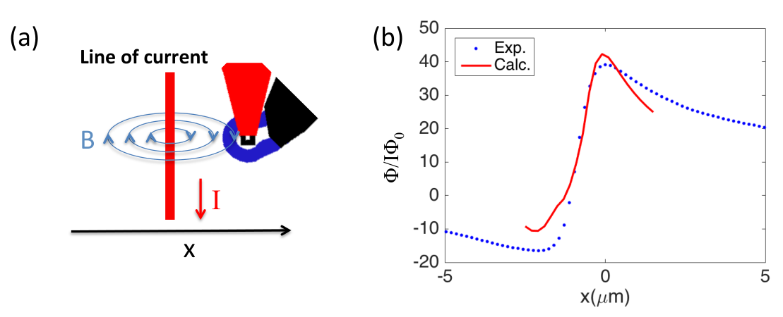
Figure 8(a) illustrates the geometry we used for testing the response of our susceptometer to a line of current. The sample was a thin strip of Pt 0.8 m wide, carrying a sinusoidally varying current with amplitude 1 mA at 500 Hz. The pickup loop leads were parallel to the current carrying strip, and perpendicular to the scan direction. The measurements were taken with the susceptometer in contact with the sample in feedback mode. The solid line in Fig. 8(b) plots the SQUID response. The open symbols are the calculations as described in Sec. 2, assuming the susceptometer was in contact with the sample, with no adjustable parameters. Although the agreement between experiment and calculation is reasonably good for the magnitude of the response, the cross-section is smeared relative to experiment, perhaps because of the finite width of the Pt strip.
4.5 Susceptibility

Finally, Figure 9(a) shows a susceptibility image of a 6 m square pillar, composed of a stack of alternating SiO2 and Nb layers 0.7 m tall. The top-most layer is Nb 0.2 m thick. This pillar is part of the fill used to make the surface flat on average to facilitate the chemical-mechanical polishing steps in producing our scanning SQUID susceptometers [18]. The image was taken at 4.2 K using a 1 mA amplitude, 500 Hz sinusoidally varying current through the field coil. The colormap scale on this image is labeled in units of the normalized change in susceptibility . The solid line in Fig. 9(b) displays a cross-section along the dashed line in Fig. 9(a). The open circles are calculations following Sec. 2 with the spacing between the surfaces of the sample and susceptometer as a fitting parameter. The best fit was for m. The calculation produces a positive overshoot to the susceptibility larger than is observed experimentally, and the spacing is larger than expected from the sample geometry and other results. We speculate that this discrepancy may be due to the 3-dimensional nature of the Nb/SiO2 pillar. Nevertheless, the calculations reproduce the width of the susceptibility transition, about 1 m from the 10% to 90% points.
Conclusions
In conclusion, we have introduced a method for calculating the response of a deep sub-micron pickup loop scanning SQUID susceptometer to external fields by solving coupled London’s and Maxwell’s equations. The results of this calculation agree reasonably well with experiments using a SQUID susceptometer with a deep sub-micron sized pickup loop for various sources of magnetic field. These calculations should provide a useful tool for interpreting scanning SQUID microscopy data with sub-micron spatial resolution.
Acknowledgements
This work was supported by an NSF IMR-MIP Grant No. DMR-0957616. J.C.P. was supported by a Gabilan Stanford Graduate Fellowship and an NSF Graduate Research Fellowship, Grant No. DGE-114747. The nanomagnet sample fabrication at Cornell was supported by the NSF (DMR-1406333 and through the Cornell Center for Materials Research, DMR-1120296), and made use of the Cornell Nanoscale Facility which is supported by the NSF (ECCS-1542081). We would like to thank Micah J. Stoutimore for providing the Nb film used to study vortices.
Citations
References
- [1] F. P. Rogers. A device for experimental observation of flux vortices trapped in superconducting thin films. Master’s thesis, Massachusetts Institute of Technology, Cambridge, Massachusetts, 1983.
- [2] L.N. Vu and D.J. Van Harlingen. Design and implementation of a scanning SQUID microscope. Applied Superconductivity, IEEE Transactions on, 3(1):1918–1921, Mar 1993.
- [3] R. C. Black, A. Mathai, F. C. Wellstood, E. Dantsker, A. H. Miklich, D. T. Nemeth, J. J. Kingston, and J. Clarke. Magnetic microscopy using a liquid nitrogen cooled YBa2Cu3O7 superconducting quantum interference device. Applied Physics Letters, 62(17):2128–2130, 1993.
- [4] J. R. Kirtley, M. B. Ketchen, K. G. Stawiasz, J. Z. Sun, W. J. Gallagher, S. H. Blanton, and S. J. Wind. High-resolution scanning SQUID microscope. Applied Physics Letters, 66(9):1138–1140, 1995.
- [5] C. Veauvy and D. Hasselbach, K .and Mailly. Scanning -superconduction quantum interference device force microscope. Rev. Sci. Instrum., 73:3825, 2002.
- [6] A. G. P. Troeman, H. Derking, B. Borger, J. Pleikies, D. Veldhuis, and H. Hilgenkamp. NanoSQUIDs based on niobium constrictions. Nano Letters, 7(7):2152–2156, 2007.
- [7] A. Finkler, Y. Segev, Y. Myasoedov, M.L. Rappaport, L. Ne?eman, D. Vasyukov, E. Zeldov, M.E. Huber, J. Martin, and A. Yacoby. Self-aligned nanoscale SQUID on a tip. Nano Letters, page 329, 2010.
- [8] Denis Vasyukov, Yonathan Anahory, Lior Embon, Dorri Halbertal, Jo Cuppens, Lior Neeman, Amit Finkler, Yehonathan Segev, Yuri Myasoedov, Michael L Rappaport, et al. A scanning superconducting quantum interference device with single electron spin sensitivity. Nature nanotechnology, 8(9):639–644, 2013.
- [9] J.R. Kirtley, B. Kalisky, J.A. Bert, C. Bell, M. Kim, Y. Hikita, H.Y. Hwang, J.H. Ngai, Y. Segal, F.J. Walker, et al. Scanning SQUID susceptometry of a paramagnetic superconductor. Physical Review B, 85(22):224518, 2012.
- [10] K. Hasselbach, D. Mailly, and J. R. Kirtley. Micro-superconducting quantum interference device characteristics. J. Appl. Phys., 91:4432–4437, 2002.
- [11] E. H. Brandt. Thin superconductors and SQUIDs in perpendicular magnetic field. Phys. Rev. B, 72:024529, 2005.
- [12] Boris Delaunay. Sur la sphere vide. Izv. Akad. Nauk SSSR, Otdelenie Matematicheskii i Estestvennyka Nauk, 7(793-800):1–2, 1934.
- [13] A. I. Bobenko and B. A. Springborn. A discrete Laplace-Beltrami operator for simplicial surfaces. ArXiv:math/0503219v3, 2006.
- [14] Mark B. Ketchen, W.J. Gallagher, A.W. Kleinsasser, S. Murphy, and John R. Clem. DC SQUID flux focuser. Technical report, International Business Machines Corp., Yorktown Heights, NY (USA). Thomas J. Watson Research Center; Ames Lab., IA (USA), 1985.
- [15] M. B. Ketchen, D. D. Awschalom, W. J. Gallagher, A. W. Kleinsasser, R. L. Sandstrom, J. R. Rozen, and B. Bumble. Design, fabrication, and performance of integrated miniature SQUID susceptometers. IEEE Trans. Mag., 25(2):1212–1215, 1989.
- [16] Brian W. Gardner, Janice C. Wynn, Per G. Björnsson, Eric W. J. Straver, Kathryn A. Moler, John R. Kirtley, and Mark B. Ketchen. Scanning superconducting quantum interference device susceptometry. Review of Scientific Instruments, 72(5):2361–2364, 2001.
- [17] Martin E. Huber, Nicholas C. Koshnick, Hendrik Bluhm, Leonard J. Archuleta, Tommy Azua, Per G. Björnsson, Brian W. Gardner, Sean T. Halloran, Erik A. Lucero, and Kathryn A. Moler. Gradiometric micro-SQUID susceptometer for scanning measurements of mesoscopic samples. Review of Scientific Instruments, 79(5):053704, 2008.
- [18] John R. Kirtley, Lisa Paulius, Aaron J. Rosenberg, Johanna C. Palmstrom, Connor M. Holland, Eric M. Spanton, Daniel Schiessl, Colin L. Jermain, Jonathan Gibbons, Y.-K.-K. Fung, et al. Scanning squid susceptometers with sub-micron spatial resolution. arXiv preprint arXiv:1605.09483, 2016.
- [19] A. Kremen, Shai Wissberg, Noam Haham, Eylon Persky, Yiftach Frenkel, and Beena Kalisky. Mechanical Control of Individual Superconducting Vortices. Nano Letters, 16(3):1626–1630, 2016.
- [20] Judea Pearl. Structure of superconductive vortices near a metal-air interface. Journal of Applied Physics, 37(11):4139–4141, 1966.