Low temperature Hall effect in bismuth chalcogenides thin films
Abstract
Bismuth chalcogenides are the most studied 3D topological insulators. As a rule, at low temperatures thin films of these materials demonstrate positive magnetoresistance due to weak antilocalization. Weak antilocalization should lead to resistivity decrease at low temperatures; in experiments, however, resistivity grows as temperature decreases. From transport measurements for several thin films (with various carrier density, thickness, and carrier mobility), and by using purely phenomenological approach, with no microscopic theory, we show that the low temperature growth of the resistivity is accompanied by growth of the Hall coefficient, in agreement with diffusive electron-electron interaction correction mechanism. Our data reasonably explain the low-temperature resistivity upturn.
Among numerous three-dimensional (3D) topological insulators, Bi2Se3 and Bi2Te3 are the most studied materials. They have a large band gap in the bulk, 300 meV and 150 meV respectively, and can be rather easily synthesized.
Revealing topological and spin related properties in these systems as a rule requires reduced temperatures. Lowering the temperature, in its turn, not merely simplifies the system, but leads to new questions. One of them is the so-called low temperature transport paradox [1]: almost all films in weak fields demonstrate positive magnetoresistance due to suppression of the weak antilocalization (WAL) correction. The WAL correction should lead to decrease of resistivity as temperature decreases (, i.e. “metallic” temperature dependence). Contrary to this expectation, almost all films, grown by various methods[2, 3, 4] and crystalline flakes split off the bulk materials [5] at low temperatures demonstrate “insulating”-type dependence () [6]. This observations mean that some other mechanism exists on top of the weak antilocalization and drives the system towards insulator as temperature decreases.
In Refs.[4, 5, 8, 9, 10, 11, 1, 7] it was conjectured that electron-electron interaction correction to conductivity could be a reason for such insulating behavior. In order to substantiate their point the authors in Refs. [4, 5, 8, 9, 10, 11, 1, 7] refer to the microscopic electron-electron interaction(EEI) theory[12, 13]. Several groups attempted to fit their transport data with EEI theory, using the Fermi-liquid coupling constant as a fitting parameter; however, the latter values extracted from fittings appeared to be very much scattered even for the samples with nominally similar carrier density.
Experimentally, the conjecture about quantitative contribution of EEI to the transport does not have a solid ground. Indeed, the EEI correction so far was extracted only in one manner: by assuming that all low- transport properties are determined by only two effects, i.e. WAL and EEI. It was assumed that subtraction of the theoretically calculated WAL contribution leaves temperature dependence of conductivity only related to the EEI correction. This assumption, however, has not been checked independently. From the theoretical point of view, all TI thin films are multi-component systems, and as it was shown e.g. in Refs. [1, 14], generalization of the electron-electron interaction correction on multi-component system is not reduced to simple results of Ref. [12]. Moreover, taking into account scattering between the subsystems further complicates the problem[15, 16]. Therefore, from fitting of the temperature dependence of the resistivity solely, one can not rule out other mechanisms on top of the WAL and EEI correction (such as, e.g., density-of-states correction [17], Maki-Thompson correction [18], etc). In order to overcome this problem we use a theoretically substantiated fully phenomenological approach, that has already been experimentally tested for disordered two dimensional systems with a simple spectrum [19].
In this paper we measure not only the temperature dependence of resistivity, but also of the Hall resistivity. We found that the low temperature growth of the resistivity is accompanied by growth of the Hall coefficient, in agreement with diffusive electron-electron interaction correction mechanism [21, 20]. We discuss only phenomenology of the EEI correction and do not address its microscopic structure. We compare two methods to determine : (i) from temperature dependence of the resistivity , similarly to the previous investigators[4, 5, 8, 9, 10, 11, 7] and (ii) from temperature dependence of the Hall resistivity . We show that in some samples and coincide, whereas in some other samples these two values deviate from each other.
I Theoretical background
The idea to determine from -dependence of the Hall resistance goes back to 1980-s, and originates from the unique property (that is independent of dimensionality) of the diffusive electron-electron interaction correction not to affect the Hall conductivity[20, 21]. In other words, for the magnetoconductivity tensor in perpendicular magnetic field one has:
| (1) |
The first term, Drude conductivity for single-component two dimensional system can be written as:
| (2) |
Inverting the conductivity tensor, and assuming that , we obtain for the resistivity tensor:
| (3) |
In the limit of low magnetic fields we come to the famous relation [21]:
| (4) |

In practice, for topological insulator thin films, the top and bottom conductive channels, and the bulk are connected in parallel and the Drude conductivity tensor is multi-component; however, this fact does not affect the low-field limit (see Appendix I). Since it is very hard to achieve mobilities exceeding 0.5 m2V-1s-1 in epitaxial films of bismuth chalcogenides [22], for most of the films the low-field linear Hall effect regime () extends to several Tesla. Another important fact is that WAL does not affect the Hall resistivity [21, 23] , i.e. one can determine EEI contribution straightforwardly by using Eq. (4), provided the temperature dependence of the Hall effect originates from EEI-correction solely.
Correspondingly, we exploit two ways to determine experimentally: (i) From the low field magnetoresistance we determine the amplitude of the WAL correction and subtract it from the low-temperature dependence. The resultant temperature dependence of the resistivity is believed to be . (ii) We analyze temperature dependence of the Hall resistance, using Eq. (4). Assuming that correction is much smaller than the Drude value of the resistivity, we get . Here the Drude value of the Hall resistance is taken at elevated temperatures, beyond the diffusive interaction regime. Since variation of the Hall resistivity with temperature is small, the particular choice of is not important. Moreover, as we can see from our data at low enough fields, thus calculated is independent.

II Experimental
We studied several samples with various mobilities, and carrier densities, their main parameters are summarized in Table 1. Epitaxial Bie3 and Bi2Te3 layers were grown on (111)-oriented BaF2 substrates similarly to Refs.[24, 25] (Bi2Se3-707 sample was grown on an Al2O3 substrate) by molecular beam epitaxy using a compound bismuth selenide/telluride effusion cell and an additional selenium/tellurium cell, respectively. Corresponding fluxes were calibrated before and after the growth using an ion gauge beam flux monitor. The beam equivalent pressure flux ratio of Se:Bi2Se3 (Te:Bi2Te3) was maintained to be 2:1 for the stoichiometry control. The film growth was performed at about 320 C at the 0.3 nm/min growth rate. Streaky RHEED patterns during the growth evidenced of single crystalline films with a smooth surface. After growth, the films on the substrate were cooled down to room temperature and 30 nm Se or 100 nm BaF2 protective cap layers were deposited on the surface of the film or the films remained unprotected (see Table 1). X-ray diffraction scans show only the allowed peaks indicating clear c-axis orientation in all the grown films. For film thicknesses ranging from 9 to 50 nm, the full width at half maximum of the (0006) rocking curve does not exceed 0.1∘ confirming high crystalline quality of the samples. Thickness of the films was determined from (0006) and (00015) Bragg peaks thickness fringes as well as from atomic force microscope measurements (see example in Fig.1d).
The studied samples were either defined lithographically as Hall bars (using Laser beam lithography system Heidelberg Pg101) and mesa-etched in oxygen plasma (see optical image in Fig.1c) or manually cut with a razor blade. Manual scratching makes geometry of the sample (see error bars in Table 1) not so well-defined, however it helps to preserve the active layer intact. The leads to the contact pads were attached with either graphite or silver paint. The results on both scratched and etched samples are similar. Charge transport in the most disordered Bi2Se3 samples showed up noise, increasing with lowering temperature (see data for sample Bi2Se3-685 below). Resistivity of all samples did not exceed 1.5 kOhm per square, so they all can be treated as “good” metals where charge transport is slightly affected by quantum corrections.
¿From the electronic transport point of view our thin films are quasi-two dimensional systems, i.e. they contain at least three interacting subsystems (two surfaces and the bulk), connected in parallel. We consider the system as two-dimensional, i.e. throughout the paper, from the measured resistance [in Ohms], we calculate resistance per square [in Ohms per square] and call it, for simplicity, “resistivity”; we further discuss corrections to its inverse value, the 2D conductivity. We believe that we can do so, because (i) in the low temperature limit the out-of-plane motion of carriers is coherent (the phase breaking length presented below much exceeds the film thickness), (ii) resistivity of our thin films very weakly responds to the parallel magnetic field, and (iii) logarithmic corrections to conductivity, observed by us and by other investigators in similar films [4, 10, 9, 8] are intrinsic to two dimensional systems solely.

Resistivity and Hall resistance were measured using standard lock-in amplifier (Hz) at temperatures 0.3-300 K and in magnetic fields up to 7 Tesla. We used PPMS-9 Tesla and Cryogenic-21 Tesla systems. Measurement current was chosen in the range 0.1-2 A to ensure the absence of overheating at the lowest temperature. In order to compensate contact asymmetry, magnetic field was swept from positive to negative values and the () data were (anti)symmetrized. Weak antilocalizaton was studied in separate low-field sweeps.
III Results
Weak field magnetoresistance due to the weak antilocalization is typically processed using the simplified Hikami-Larkin-Nagaoka(HLN) formula:
| (5) |
Here is the phase coherence length and is the prefactor, i.e. adjustable parameter that denotes a number of WAL channels. This formula is applicable in the so-called diffusive transport regime, i.e. when both and magnetic length much exceed the mean free path . Figure 1 shows examples of magnetoconductance due to WAL for sample Bi2Se685 and their fits with HLN formula. Similarly to Refs. [4, 11, 26, 27], we find that the prefactor is close to 0.5 and does not demonstrate temperature dependence (average prefactors are summarized in Table 1), indicating strong spin-orbit coupling. The phase coherence length is roughly proportional to , as it should be for dephasing caused by electron-electron scattering [21], similarly to observations of Refs. [4, 26, 27, 5], The zero-field temperature dependence of the resistivity due to WAL is expressed as:
| (6) |
The amplitude of thus determined WAL correction is shown by black stars in Figs. 3, 4a, 5a. Alternatively, WAL contribution might be estimated similarly to Refs.[7, 10] as a difference of conductivities at and at some elevated magnetic field , where dependence of the WAL is already suppressed: . Interestingly, the results obtained by this method (empty stars in Figs.2, 4a, 5a) with reasonable precision coincide with those obtained from data fitting with Eqs. (5) and (6).
| Sample, | n, | ,cm2 | , | Comment | ||||||
| cm-2 | V-1s-1 | Ohm/ | m | m | nm | |||||
| Bi2Se3-724 | 5.9 | 5000 | 205 | 56050 | 1655 | 10 | 0.33 | 1.6 | 1.6 | Se-covered, scratched |
| Bi2Se3-685 | 61 | 85 | 1170 | 125 | 80 | 15 | 0.5 | 3.10.3 | 3.10.3 | mesa-etched |
| Bi2Se3-691 | 140 | 37 | 1216 | 120 | 75 | 18 | 0.5 | 2.5 | 2.8 | unprotected, mesa-etched |
| Bi2Te3-677 | 62 | 630 | 160 | 460 | 125 | 23 | 0.7 | 1.4 | 1.95 | 12 nm BaF2-covered, scratched |
| Bi2Se3-707 | 61 | 410 | 245 | 770 | 195 | 17 | 0.65 | 1.4 | 3.25 | Al2O3 substrate, scratched |
The effect of EEI correction for the low mobility mesa-etched sample Bi2Se3-685 is the most pronounced: Figure 2 shows magnetoresistance and Hall effect versus magnetic field in a wide range of temperatures. As magnetic field increases, there is a weak positive temperature-independent MR on top of WAL. This MR is a consequence of several parallel conducting channels with various mobilities (bulk and surfaces, see Appendix I). Hall resistance is linear-in- and has an interesting feature: the Hall slope grows with decrease of temperature, as it is clearly seen from Fig. 2. Such huge variation of the Hall slope with temperature ( - see insert to Fig. 2) would be prohibited by overall electro-neutrality of the system were the Hall resistance related to the inverse carrier density; however it is possible that the EEI correction comes into play and should be added to the Drude conductivity, as Eq. (3) suggests.
If we interpret the temperature-dependent part of the Hall slope within Eq. (4) [for more details, see section “Theoretical background”, method (ii)], we directly get temperature dependence of the EEI correction and may use it for comparison with the corresponding variation of the resistivity ( triangles in Fig. 3). When we subtract WAL (stars in Fig. 2) from the dependence, we get almost indistinguishable temperature dependence of the resistivity (see circles in Fig. 2). The observed agreement is the one of the central results of our paper. Moreover, this temperature dependence is visibly logarithmic, , and our observation means that .
The value of is enormously large and exceeds those reported in Refs. [8, 9, 10, 11, 7]. Moreover, even within the theoretical predictions [1] there is no way to obtain more than 2. A possible physical origin of the enhanced could be effective decoupling of conductive channels. This mechanism was suggested in Ref. [4], where was also observed. Indeed, for such high electron densities, many quantization subbands are filled. If all these subbands generated independent conductive channels, each of them should have its own EEI correction to conductivity , with . In this case the total EEI correction should be a sum of all contributions and may be large. In practice, however, electrons from different subbands interact with each other and the amount of singlet terms may be reduced to one. The question why in this particular sample Bi2Se3-685 (and probably Bi2Se3-691, see Table 1) such interaction is suppressed remains opened.
Importantly, the coincidence of and is not occasional, rather, it is observed in several samples (see Table 1). For example, sample Bi2Se3-724 (see Fig. 4) contains high mobility (presumably surface) carriers atop of low-mobility (presumably bulk) carriers. As a result, its Hall coefficient visibly drops with field (see Appendix I) starting from already Tesla (see Fig. 4b). Nevertheless, temperature dependence of the Hall effect is easily seen, its relative variation is almost -independent (here is the magnetic field at which Hall effect is analyzed), and we again get .
The prefactor has a reasonable value of about 0.33. Similar values of were also reported in Refs. [4, 10]. The value of is also comparable with those observed in Ref. [10]. Both non-ideal and values were explained theoretically in Ref. [1]. Prefactor might also differ from 0.5 because the effective ratio for sample made by scratching, might be determined only roughly; however within our phenomenological approach this uncertainty does not modify the overall result (see discussion below and Appendix II).

We note that the coincidence of and is not observed universally in all samples. For example, Fig. 5 shows temperature dependence of the resistivity, WAL, and Hall effect in bismuth telluride sample Bi2Te3-677 with the same carrier density as Bi2Se3-685 and an order of magnitude higher mobility. In bismuth telluride, the phonon-scattering-limited metallic temperature dependence of the resistivity is much stronger and extends to much lower temperatures.
Correction to the Hall coefficient is logarithmic in temperature (see Fig. 5b recalculated using Eq. (4) to blue triangles in Fig.5a), but this temperature dependence is even weaker than the temperature dependence of resistivity. If we subtract WAL from the resistivity, we get circles in Fig. 5a with stronger temperature dependence. In other words is about factor of two larger than . Possible reasons for the difference are discussed below. At the same time, the WAL prefactor in this sample has a reasonable and -independent value of 0.7 (see Fig. 6c). Bi2Se3-707 sample is pretty much similar to Bi2Te3-677.

IV Discussion
Importantly, inexact definition of the sample geometry by scratching (see example in the inset to Fig. 5a) does not affect the results obtained within our phenomenological approach. Indeed, according to Eq. 4, correction to the Hall coefficient is recalculated directly to the correction to diagonal resistance. When evaluating WAL contribution we measure prefactor using Eq. 5 and then substitute the result with the same prefactor into Eq.6. If the geometrical factor ( in case of the Hall bar geometry) is calculated incorrectly, we automatically get the modified value of , but the total contribution of WAL in temperature dependence of the resistivity, calculated using Eq. 6 will remain correct. Observation of in almost all cases means that we are not mistaken with ratio.
Remarkable property of both WAL and EEI corrections is their logarithmic temperature dependence. This logarithm has a high temperature cut off when the corresponding length (interaction or phase breaking) becomes comparable with the mean free path (in our samples this equality corresponds to 10-300 K, i.e. above the resistivity minimum temperature). In this low temperature limit we neglect temperature dependence of the mean free time. The functional dependence of the result for the amplitude of both WAL corrections to conductivity and EEI correction is similar: the amplitude is roughly proportional to (i)the corresponding amplitude factor of the order of unity ( in case of WAL, and Fermi-liquid coupling dependent term in case of EEI), (ii) [21, 19] in case of EEI (where is the mean free time), and in case of WAL. is usually inversely proportional to temperature, therefore we get the same dependence. Since , the main parameter that governs the amplitude of the correction to resistivity is the sheet resistance value. Indeed, in Fig. 2 for Bi2Se3-685 with resistivity about 1 kOhm per square we see huge variation of the resistivity with temperature (about 10% i.e. 100 Ohm), whereas for Bi2Se3-724 with resistivity about 200 Ohm per square (see Fig. 4) the overall variation of resistivity is about 0.5%, i.e. 1 Ohm.
It should be discussed why the data for samples Bi2Te3-677 and Bi2Se3-707 deviate from those for the other bismuth selenides. Naively, the difference between Bi2Te3 and Bi2Se3 thin films is as follows: (i) selenides are n-doped, whereas sample Bi2Te3-677 is p-doped; (ii) spectra of carriers in Bi2Te3 are hexagonally wrapped. This wrapping was shown to modify the ordinary low-temperature resistivity behavior [29]. It is not clear whether the wrapping somehow affects EEI correction to conductivity. Close similarity between Bi2Te3-677 and Bi2Se3-707 samples does not support the latter possibility.
The agreement between resistivity and Hall resistivity in these samples would become much better if instead of Eq. (4) one would use . Such functional temperature dependence of the Hall effect might originate from variable number of carriers; this mechanism was suggested, e.g., in Refs. [31, 30]. Indeed, if only one group of high mobility carriers determines transport, then , and . Variation of in this case leads to , contrary to Eq. (4). Nevertheless, we think that this mechanism is irrelevant here, because we clearly observe logarithmic temperature dependence of the Hall effect, instead of the expected exponential activated dependence [31, 30].
In fact, the lack of quantitative agreement with quantum correction theory is not surprising because of the complexity of the studied films, and was observed several times even for systems with much simpler spectrum [19, 32]. As a possible clue to the explanation of this discrepancy, the prefactor was found to be unexpectedly high in samples Bi2Te3-677 and Bi2Se3-70. Theoretically (see [1] and references therein) one expects . Observation of the anomalous prefactor value out of this interval means that the sample is more complicated than the naive model presumes. There are many unexplored factors, whose effect on transport properties of bismuth chalcogenides is not yet explored, e.g. formation of Bi- bilayers [37], spatial inhomogeneity, surface oxidation and irreproducible band-bending [36], intersubband scattering, etc. The task of the further studies will be to understand why the validity of Eq. (4) in quantum transport is sample-dependent.
values for the majority of our samples is comparable with those measured by other groups [4, 5, 11, 9, 10], whereas the temperature dependence of the Hall effect in these papers was not analyzed. However, in Ref. [31] [7 nm film shown in Fig. 4(a) and 4(d)], and in Ref. [33] (Fig. 8), one can see correlation between the low- resistivity upturn and increase of the Hall coefficient; remarkably, the resistivity per square for these films and the scale of the Hall coefficient variation are comparable to those for our samples.
In several papers[9, 11], attempts have been made to deduce EEI correction from its Zeeman splitting dependence by applying magnetic field parallel to the sample plane and comparing the data with the classical theory by Lee and Ramakrishnan [13]. Two notes should be made here: (i) straightforward application of the Lee and Ramakrishnan theory [13] to chalcogenides is not justified, because even without Zeeman splitting, the electron-electron interaction in multi-component carrier system in topological insulator is not simple [1, 14]. Possible scattering between bulk and surface states and between the opposite surface states will further complicate EEI correction, similarly to the multi-valley system [15, 16]. Moreover, in case of a strong spin-orbit coupling, triplet terms of the EEI correction are already suppressed, and additional Zeeman splitting is not expected to affect EEI correction [21]. (ii) Experimentally Zeeman effect on the EEI correction in topological insulators can be revealed and disentangled from all other possible orbital effects by temperature dependence of the Hall effect in the presence of Zeeman field. Similar measurements were already performed in two-dimensional system with ordinary spectrum [32].
V Conclusions
We have shown that in various thin films of Bi2Te3 and Bi2Se3 topological insulators, the low temperature Hall coefficient shows a logarithmic temperature correction. In several samples the low- behavior of both resistivity and Hall effect was consistently quantitatively explained by only two mechanisms: weak anti-localization and electron-electron interaction correction, with the latter being dominant in temperature dependence of the resistivity. We have come to this conclusion by using only the phenomenological property of the electron-electron interaction correction not to affect the Hall conductivity. Thus, our method is an alternative way to determine the electron electron interaction constant . On the basis of our data it is impossible to say where the EEI correction comes from: topological surface states or bulk. In our studies, we tested the robustness of the relationship between the corrections to Hall resistance and diagonal resistivity for samples with different mobility, substrate, and composition. As a result we found that the agreement with interaction correction theory is perfect in some cases and imperfect in other. However, we didn’t reveal a strong contradiction with theory and this one of our main findings.
Our study poses new questions: Why amplitude of the electron-electron interaction correction to conductivity in high-density low-mobility films is so large? Why in some samples the phenomenological agreement between experimental data and theory of quantum corrections is not perfect? A practical consequence of our results is that the Hall slope in topological insulator thin films does not exactly correspond to carrier density: it includes quantum correction that may be as high as few 10 in low-mobility films and should be taken into account.
VI Acknowledgements
We thank I. S. Burmistrov and G.M.Minkov for discussions. The work was supported by RFBR (16-29-03330). VAP also acknowledges the Indian-Russian Grant DST-MSE 14.613.21.0019 (RFMEFI61314X0019) for support. Magnetotransport measurements have been done using research equipment of the LPI Shared Facility Center.
VII APPENDIX I. ELECTRON-ELECTRON INTERACTION CORRECTION TO CONDUCTIVITY IN MULTY-COMPONENT SYSTEM.
In this section we consider conductivity of a multi-component system in the presence of EEI correction. We assume that the property Eq. (1) for the EEI correction is valid and the classical part of the conductivity tensor is just a sum of the contributions from all components, i.e:
| (7) |
Here is the number of conductive channels. The calculations of the inverse tensor are trivial but very lengthy. We therefore restrict ourselves to two relevant cases. The first case is the low-field limit for all . In this limit we can neglect all quadratic in field terms and consider only linear-in- Hall resistance. Correspondingly, we have:
| (8) |
| (9) |
It is easy to see that Eq. (4) is fulfilled also in the multi-component system. Another case, related to sample Bi2Se3-724, considers high-mobility sample, where condition is not fulfilled. In order to avoid cumbersome formulas we consider and assume a small density of high-mobility () surface electrons and much larger density of bulk electrons. The linear in field terms of Hall resistance are given by Eq. (9), while for cubic-in-field terms, neglecting we have:
| (10) |
This equation means that not only linear in field term in Hall resistivity should slightly vary with temperature, but also cubic-in-field one. Indeed, as it can be obtained from Fig.4b, the slope of the versus increases by as temperature increases from 0.3 K to 30 K. This effect appears to be too small to identify logarithmic dependence, although the sign of the effect agrees with Eq. (10). We believe that taking higher order terms and more groups of carries into account one would make the agreement better.
VIII APPENDIX II. ESTIMATES OF ERRORS.
In our case there are two types of errors: systematic and random. The systematic ones are related to the uncertainty of the geometry, i.e. to the definition of ratio. In Fig. 6a we demonstrate that the average width fluctuates across the sample, correspondingly conductivity recalculated from the resistance has an uncertainty (about 10-15% in all scratched samples). As a result both and has the same geometrical uncertainty (). Nevertheless this type of error does not affect mutual relations between various mechanisms, or between , determined from different methods, i.e. it does not affect the main statement of the paper.
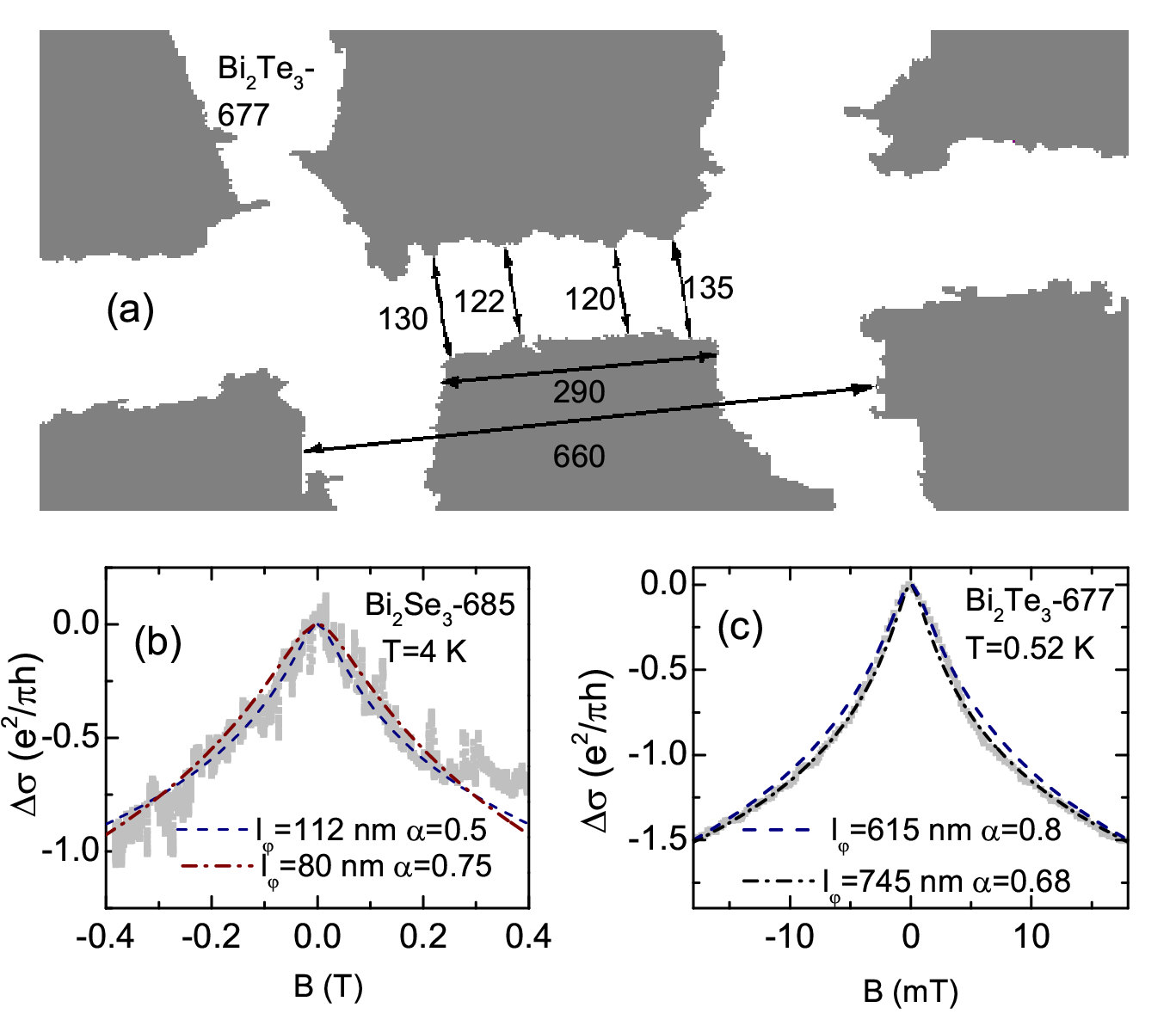
Random errors in our case come from several sources: (1) The errors related to spread of values at different temperatures, or spread of values used for linear interpolation. (2) For lithographically defined low-mobility samples the resistivity signal was noisy (see e.g., Fig. 1). Such noise might come from bulk carriers [34, 35] or from unstable contacts. Sometimes resistivity exhibited jumps (see e.g. 4 K and 16 K curves in Fig. 1), that makes the overall fitting procedure ill-defined, because the fit is non-linear and depends on symmetrization, definition of resistivity, and the field range used for fitting. The best thing we can do is to play manually with all these parameters, find and by minimizing the the standard deviation in each case and see how these parameters are scattered. Fig. 6b illustrates that the noisy data cause large uncertainty in the determined and values: indeed to make WAL curve fit visibly distinguishable from the experimental data one has to vary by 50% and by 30%. For comparison we show in Fig. 6c the data for much cleaner sample, where variations of and are significantly smaller.
Having estimated all types of errors we evaluate the error of or as:
| (11) |
| (12) |
These values are indicated in Table 1.
References
- [1] Hai-Zhou Lu, Shun-Qing Shen, Phys. Rev. Lett 112, 146601 (2014).
- [2] Y. H. Liu, C. W. Chong, J. L. Jheng, S. Y. Huang, J. C. A. Huang, Z. Li, H. Qiu, S. M. Huang, and V. V. Marchenkov,Appl. Phys. Lett. 107, 012106 (2015).
- [3] Min Zhang, Li Lv, Zhantao Wei, Cunsheng Guo, Xinsheng Yang, Yong Zhao, Materials Letters 123 8789, (2014).
- [4] W.J. Wang, K.H. Gao, Z.Q. Li, Scientific Reports, 6, 25291 (2016)
- [5] Shao-Pin Chiu and Juhn-Jong Lin, Phys. Rev. B 87, 035122 (2013).
- [6] For a review, see: S. Q. Shen, Topological Insulators (Springer-Verlag, Berlin, 2012).
- [7] H.C. Liu, H.Z. Lu, H.T. He, B. Li, S.G. Liu, Q.L. He, G. Wang, I.K. Sou, S.Q. Shen, J. Wang, ACS Nano, 8, 9616-9621 (2014).
- [8] M. Liu, C.Z. Chang, Z. Zhang, Y. Zhang, W. Ruan, K. He, L.L. Wang, X. Chen, J.F. Jia, S.C. Zhang, Q.K. Xue, X. Ma, Y. Wang, Phys. Rev. B 83, 165440 (2011).
- [9] J. Wang, A. M. DaSilva, C. Chang et al, Phys.Rev. B, 83, 245438, (2011).
- [10] Y. Takagaki, B. Jenichen, U. Jahn, M. Ramsteiner, K.J. Friedland, Phys.Rev. B, 85, 115314, (2012).
- [11] R. Dey, T. Pramanik, A. Roy, A. Rai, S. Guchhait, S. Sonde, H. C. P. Movva, L. Colombo, L. F. Register, S. K. Banerjee, Appl. Phys. Lett. 104, 223111 (2014).
- [12] B. L. Altshuler, A. G. Aronov, and P. A. Lee, Phys. Rev. Lett. 44, 1288 (1980).
- [13] P.A. Lee, T.V. Ramakrishnan, Phys. Rev. B26 , 4009 (1982).
- [14] E. J. Konig, P. M. Ostrovsky, I. V. Protopopov, I. V. Gornyi, I. S. Burmistrov, and A. D. Mirlin, Phys. Rev. B 88, 035106 (2013).
- [15] Alexander Punnoose; Phys. Rev. B 81, 035306 (2010).
- [16] A. Yu. Kuntsevich, N. N. Klimov, S. A. Tarasenko, N. S. Averkiev, V. M. Pudalov, H. Kojima, and M. E. Gershenson, Phys. Rev. B 75, 195330, (2007).
- [17] A.I. Larkin, Pisma Zh. Eksp. Teor. Fiz. 31, 239 (1980). [Sov. JETP Letters 31, 219 (1980)].
- [18] K. Maki, Progr. Theor. Phys. 39, 897 (1968); R.S. Thompson, Phys. Rev. B 1, 327 (1970).
- [19] G.M. Minkov, O.E. Rut, A.V. Germanenko, A.A. Sherstobitov, V.I. Shashkin, O.I. Khrykin, and V.M. Daniltsev, Phys. Rev. B 64, 235327 (2001).
- [20] B. L. Altshuler, D. Khmel’nitzkii, A. I. Larkin, and P. A. Lee, Phys. Rev. B 22, 5142 (1980).
- [21] B. L. Altshuler, A. G. Aronov. Electron-electron interaction in disordered conductors. in Electron-Electron Interaction in Disordered Systems, Edited by A. L. Efros and M. Pollak (North Holland, Amsterdam) pp. 1-153, 1985.
- [22] N. Koirala, M. Brahlek, M. Salehi, L. Wu, J. Dai, J. Waugh, T. Nummy, M.-G. Han, J. Moon, Y. Zhu, D. Dessau, W. Wu, N.P. Armitage, S. Oh, Nano Lett., 15(12), 82458249, (2015).
- [23] H. Fukuyama. J. Phys. Soc. Jap.,49, 644-648, (1980)
- [24] O. Caha, A. Dubroka, J. Humlicek, V. Holy, H. Steiner, M. Ul-Hassan, J. Sanchez-Barriga, O. Rader, T. N. Stanislavchuk, A. A. Sirenko, G. Bauer, G. Springholz. Cryst. Growth Des., 13, 3365, (2013).
- [25] K. Hoefer, C. Becker, D. Rata, J. Swanson, P. Thalmeier, L. H. Tjeng. PNAS, 111, 14979, (2014).
- [26] J. Chen, X. Y. He, K. H.Wu, Z. Q. Ji, L. Lu, J. R. Shi, J. H. Smet, and Y. Q. Li, Phys. Rev. B 83, 241304(R), (2011).
- [27] A. A. Taskin, Satoshi Sasaki, Kouji Segawa, and Yoichi Ando, Phys. Rev. Lett. 109, 066803 (2012).
- [28] N. Bansal, Y.S. Kim, M. Brahlek, E. Edrey, S. Oh, Phys. Rev. Lett. 109, 116804, (2012).
- [29] H.K. Pal, V.I. Yudson, D.L. Maslov, Phys. Rev. B 85, 085439, (2012).
- [30] A. Yu. Kuntsevich, D. A. Knyazev, V. I. Kozub, V. M. Pudalov, G. Brunthaler, and G. Bauer, JETP Lett., 81, 409 (2005).
- [31] L. He, F. Xiu, Y. Wang, A.V. Fedorov, G. Huang, X. Kou, M. Lang, W.P. Beyermann, J. Zou, K.L. Wang, Jour. of Appl. Pphys 109, 103702 (2011).
- [32] A. Yu. Kuntsevich, L. A. Morgun, and V. M. Pudalov, Phys. Rev. B 87, 205406 (2013).
- [33] J. Barzola-Quiquia, T. Lehmann, M. Stiller, D. Spemann, P. Esquinazi, P. Hussler, Journal of Applied Physics, 117, 075301,(2015).
- [34] S. Bhattacharyya, M. Banerjee, H. Nhalil, S. Islam, C. Dasgupta, S. Elizabeth, A. Ghosh, ACS Nano, 9, 12529-12536 (2015).
- [35] T. Trivedi, S. Sonde, H. C. P. Movva, S. K. Banerjee, Journal of Applid Physics 119, 055706 (2016).
- [36] B. Skinner, T. Chen, and B. I. Shklovskii, Phys. Rev. Lett. 109, 176801 (2012).
- [37] P. M. Coelho, G.A.S. Ribeiro, A. Malachias, et al, Nano Lett., 13, 4517, (2013)