Vibrational and optical properties of MoS2: from monolayer to bulk
Abstract
Molybdenum disulfide, MoS2, has recently gained considerable attention as a layered material where neighboring layers are only weakly interacting and can easily slide against each other. Therefore, mechanical exfoliation allows the fabrication of single and multi-layers and opens the possibility to generate atomically thin crystals with outstanding properties. In contrast to graphene, it has an optical gap of 1.9 eV. This makes it a prominent candidate for transistor and opto-electronic applications. Single-layer MoS2 exhibits remarkably different physical properties compared to bulk MoS2 due to the absence of interlayer hybridization. For instance, while the band gap of bulk and multi-layer MoS2 is indirect, it becomes direct with decreasing number of layers. In this review, we analyze from a theoretical point of view the electronic, optical, and vibrational properties of single-layer, few-layer and bulk MoS2. In particular, we focus on the effects of spin–orbit interaction, number of layers, and applied tensile strain on the vibrational and optical properties. We examine the results obtained by different methodologies, mainly ab initio approaches. We also discuss which approximations are suitable for MoS2 and layered materials. The effect of external strain on the band gap of single-layer MoS2 and the crossover from indirect to direct band gap is investigated. We analyze the excitonic effects on the absorption spectra. The main features, such as the double peak at the absorption threshold and the high-energy exciton are presented. Furthermore, we report on the phonon dispersion relations of single-layer, few-layer and bulk MoS2. Based on the latter, we explain the behavior of the Raman-active and modes as a function of the number of layers. Finally, we compare theoretical and experimental results of Raman, photoluminescence, and optical-absorption spectroscopy.
1 Introduction
For many layered materials, it has been established that the few-layer or mono-layer phases have distinct properties with respect to their bulk counterparts. Often these properties are even changing between the mono-, bi- and, tri-layer phases. Within the layers, the atoms are held together by strong covalent bonds while the inter-layer bonds are rather weak and mostly due to van der Waals interaction. As a consequence, the layers can easily be separated by mechanical exfoliation and single, quasi two-dimensional (2D), and few-layer systems of various materials can easily be produced.[1] Some examples are graphene, hexagonal boron nitride (BN), semiconducting transition metal dichalcogenides (M = Mo, W, Ta, and X = S, Se, Te), [2] the superconducting metal , or the elemental 2D systems silicene, germanene, and phosphorene [3].
Many of these materials have potential for novel technological functionalities. Graphene is the most prominent single-layer material [4]. It does not only have outstanding physical properties such as high conductivity, flexibility, and hardness [5], but it is also a benchmark for fundamental physics. E.g., it displays an anomalous half-integer Quantum Hall effect due to the quasi-relativistic behavior (linear crossing in the band-structure) of the -electrons[6, 7]. The fascinating properties of graphene have paved the way for intense investigations of alternative layered materials.[1]
Electronics and optical applications often require materials with a sizeable band gap. For instance, the channel material in field-effect transistors must have a sufficient band gap to achieve high on/off ratios [8]. In this respect, the semiconducting transition metal dichalcogenides (TMDs) can complement or substitute the zero-band gap material graphene[9]. Single-layer is an appealing alternative for opto-electronic applications with an optical gap of 1.8-1.9 eV, high quantum efficiency[10, 11], an acceptable value for the electron mobility[12, 13], and a low power of dissipation[14]. It has potential application in nanoscale transitors [9, 15, 12, 8], photodetectors [16, 17], and photovoltaics applications [18, 19, 20]. Other TMDs such as single-layer also exhibit high photoluminescence yield [21].
In this stimulating scenario, TMDs are being intensively investigated. Fabrication techniques such as the mechanical exfoliation [22, 23] and the liquid exfoliation [24] produce single- and multi-layer crystals with high crystalline quality at low cost. This has increased notably the amount of research groups working in both fundamental and applied aspects of TMDs. Concerning the electrical and optical properties of single-layer, multi-layer and bulk , extensive experimental investigations have been carried out within the last few years. The most important techniques are photoluminescence, optical absorption, and electroluminescence spectroscopy [10, 11, 25, 26]. It is widely accepted that single-layer has a direct band gap that transforms into an indirect gap with increasing number of layers. Similarly, bandgap engineering is possible by applying strain. The application of strain drives a direct-to-indirect band gap transition in single-layer [27, 28, 29, 30, 31, 32]. Moreover, suitable hydrostatic pressure reduces the band gap of single- and multi-layer resulting in a phase transition from semiconductor to metal [33, 34]. The group symmetry and the spin-orbit interaction in also raise interesting properties. The control of the valley polarization of the photo-generated electron-hole pairs paves the way for using in applications related to next-generation spin- and valleytronics [35, 36, 37, 38, 39]. Further studies dealing with charged exciton complexes (trions)[40, 41] or with second harmonic generation have also been published [42, 43].
Many challenges remain to be solved in the field of TMDs. The problem of obtaining high hole mobility in single-layer hinders the realization of p-n diodes. A proposed solution is using a monolayer diode, in which the p-n junction is created electrostatically by means of two independent gate voltages [20, 44, 45]. Another active research field is the design of Van der Waals heterostructures. Assembling atomically thin layers of distinct 2D materials allows to enrich the physical properties [46]. Techniques like chemical vapor deposition and wet chemical approaches are triggering the fabrication of heterostructures [47, 48]. For example, flexible photovoltaic devices of TMDs/graphene layers exhibit quantum efficiency above 30% [49]. A photovoltaic effect has also been achieved using a p-n heterojunction [19]. The different stacking configurations and the band alignments are important aspects in bilayer heterostructures[50, 51, 52].
Another important activity in the field of TMDs is the characterization of the vibrational properties of . Earlier studies of bulk using Raman and infrared spectroscopy [53, 54] as well as Neutron scattering[55] and electron-energy-loss spectroscopy[56] had already well characterized the phonons at and the phonon dispersion. In the recent years, a large number of Raman studies on mono- and few-layer systems has emerged [57, 58, 59, 60, 61, 62, 63, 64, 65]. The Raman frequencies are correlated with the number of layers which allows their unequivocal identification. The trend of the Raman modes (in-plane mode) and (out-of-plane mode) with the number of layers has been intensively discussed, both theoretically [66, 67, 62, 68] and experimentally [57, 69, 68]. The mode follows a predictable behavior. Its frequency grows with increasing number of layers, due to the interlayer interaction. The mode shows the opposite trend, i. e., decreasing in frequency for an increasing number of layers.
The experimental findings are accompanied by a vast theoretical literature. The characteristic stacking of ultra-thin layers of adds new challenges to the theoretical approaches. For example, the layer thickness influences the dielectric constant which becomes strongly anisotropic. This enhances the Coulomb interaction between carriers. The calculation of the excitations has to include these dimensional effect for applying accurately the GW method and the Bethe-Salpeter equation. For instance, one consequence is an exciton binding energy in some layered materials of hundreds of meV, much larger than in bulk semiconductors. Also, new models have been developed to explain the interplay of the spin-orbit interaction and the crystal symmetry (which is layer dependent), and its consequences, like the valley-Hall effect. Moreover, the interlayer interaction has demanded the improvement of the modelling of the van der Waals interaction in extended systems. The precision of the Raman spectroscopy has allowed to evaluate the accuracy of ab initio methods for calculating phonons, and it proves how useful is the simulation of the vibrational properties for understanding the interlayer interaction and the chemical bonding. Therefore, the research on layered materials has contributed to the appeareance of new methods and to the reformulation of existing ones. In this review, we give an overview of the challenges in the modelling of the spectroscopic properties of and the solutions proposed. The discussion of the literature results is complemented by additional calculations. We believe the topics discussed here will be also useful in the modelling and understanding of other two-dimensional materials.
2 Structural properties

Bulk molybdenum disulfide () belongs to the class of transition metal dichalcogenides (TMDs) that crystallize in the characteristic 2H polytype. The corresponding Bravais lattice is hexagonal and the space group of the crystal is ( non-symmorphic group). The unit cell is characterized by the lattice parameters (in-plane lattice constant) and (out-of-plane lattice constant). The basis vectors are
| (1) |
The unit cell contains 6 atoms, two Mo atoms are located at the Wyckoff sites and four S atoms at the Wyckoff sites. With the internal parameter , the positions, expressed in fractional coordinates, are (1/3, 2/3,1/4) for the Mo atoms and (2/3, 1/3,) as well as (2/3, 1/3,1/2-) for the S atoms.
The single-layer contains one Mo and two S atoms. In this case, the inversion symmetry is broken and the space group (more precisely, layer group) is ( symmorphic group). The double-layer is constructed by adding another S-Mo-S layer, having now the layer group ( symmorphic group). Consequently, an odd number of layers has the same symmetry as the single-layer (absence of inversion symmetry), whereas an even number has the symmetry of a double-layer (with inversion symmetry).
| (Å) | (Å) | (GPa) | |||
| Ref. [70] | 3.160 | 12.294 | 0.621 | 3.890 | |
| Ref. [71] | 3.161 | 12.295 | 0.627(5) | 3.890 | |
| Ref. [72] | 3.140 | 12.327 | 3.926 | 53.41.0 | |
| Ref. [73] | 3.168(1) | 12.322(1) | 0.625 | 3.890 | |
The crystal structure of can be specified as a stacking of quasi-two-dimensional (2D) S-Mo-S layers along the direction. Within each layer, Mo atoms are surrounded by 6 S atoms in a trigonal prismatic geometry as illustrated in Fig. 1. The bonding type is predominantly covalent within the atomically thin S-Mo-S layers, whereas the layers themselves are weakly bound by Van der Waals (VdW) forces in the crystal. The inherent weakness of the interlayer interactions can result in different stacking sequences and therefore in different polytypisms as shown in Ref. [74].
Defining the optimized geometry is the first step for any calculation of the phonon spectra and/or the band structure. Most of the previous investigations used density-functional theory (DFT) on the level of the local-density approximation (LDA) or the generalized-gradient approximation (GGA) [66]. We want to emphasize that in DFT the accuracy of the calculated quantities is determined by the treatment of the exchange correlation (XC) energy given by the XC functional. However, the standard local (LDA) and semilocal (GGA) XC functionals do not account for the long-range van der Waals interactions, which are responsible for the stable stacking of the layers and thus particularly relevant in two-dimensional materials. Nevertheless, the well-known LDA overestimates the (weak) covalent part of the interlayer bonding and compensates thus the missing vdW forces yielding a bound ground state for most layered materials. This explains the success of LDA in obtaining the geometry of many layered materials such as graphite [75], boron nitride [76, 77] or graphene on different substrates [78, 79, 80]. The good performance of LDA in layered materials (although fortuitous) has made this approximation widely used in the calculations of structural properties.
In the present work, the calculations were partly performed with the Vienna ab initio simulation package (VASP)[81, 82] utilizing the projector augmented plane wave (PAW) method [83, 84] to describe the core-valence interaction. PAW potentials with non-local projectors for the molybdenum (Mo) 4, 4, 4, 5 as well as sulfur (S) 3, and 3 valence states were generated to minimize errors arising from the frozen core approximation. The valence electrons were treated by a scalar-relativistic Hamiltonian and spin orbit coupling (SOC) was self-consistently included in all VASP calculations as described elsewhere [85]. VASP uses DFT with a variety of XC functionals ranging from LDA to different types of GGAs, to hybrid functionals, and VdW density functionals. Furthermore, VASP has an implementation of many body perturbation theory such as the approximation ranging from the single-shot [86] to a selfconsistent (sc) approximation[87, 88]. Concerning standard DFT results presented in this work, the XC energy was treated within the LDA[89] and the GGA. For the latter, the parametrization of Perdew, Burke, and Ernzerhof (PBE), in particular the PBEsol functional [90] was used.
In order to improve the theoretical lattice parameters calculated within DFT-LDA/GGA[66], we have also studied the structural properties including VdW interactions starting from the experimentally observed structural parameters summarized in Tab. 1. For this purpose we used the optB86b-VdW functional, recently implemented in VASP [91]. The optB86b functional is a non-local correlation functional that approximately accounts for dispersion interactions. It is based on the VdW-DF proposed by Dion et al.[92], but employs an accurate exchange functional particularly optimized for the correlation part. [91]
The structural optimization of hexagonal bulk requires a 2D energy minimization, since the ground state energy depends on two degrees of freedom, i. e., the volume and the ratio. The experimentally observed structural parameters summarized in Tab. 1 have been used as starting point for the calculation of the electronic properties of bulk as well as single layer (1L) within DFT and methods that go beyond as described in detail below. This minimization was performed manually using LDA and PBEsol as well as the optB86b-VdW functional, for comparison by varying the unit cell volume of bulk within of the experimentally observed equilibrium volume (). For each chosen volume the ratio was first optimized by fitting the energy dependence on to the Murnaghan equation of state (EOS). [93] The final DFT-optimized unit cell volume was obtained by subsequently fitting to the Murnaghan EOS. Note that in each single optimization step the atomic positions were also relaxed by minimizing the total forces on the atoms until they were converged to 0.05 eV/Å.
In order to avoid effects from the changes in size of the basis set due to changes in the unit cell volume , the kinetic energy cutoff has been increased to 350 eV. Convergence with respect to sampling within the Brillouin zone was reached with -centered meshes in case of optB86b-VdW and with -centered meshes for LDA and PBEsol. The manually performed structural optimization was cross checked with VASP calculations employing minimization algorithms parallel for the atomic positions and the ratio for selected volumes in the range of and one subsequent Murnaghan EOS fit. From these calculations the Bulk modulus is obtained from
| (2) |
In Table 2 the results of the structure optimization corresponding to different functionals are summarized.
| (Å) | (Å) | (GPa) | (Å) | VdW gap (Å) | |||
|---|---|---|---|---|---|---|---|
| LDA | 3.120 | 12.09 | 0.1214 | 3.87 | 40-43 | 6.039 | 2.933 |
| PBEsol | 3.138 | 12.60 | 0.1264 | 4.01 | 18-21 | 6.305 | 3.188 |
| optB86b-VdW | 3.164 | 12.40 | 0.1236 | 3.92 | 39-40 | 6.203 | 3.068 |
When using LDA or optB86b-VdW functionals, the theoretical values of for bulk agree well with the experimental value given in Table 1. Concerning lattice parameters, we observe a small underestimation of the in-plane parameter , both in LDA (1.3 %) and PBEsol (0.7 %). Contrary, the parameter is underestimated by 1.6% and overestimated by 2.4% in LDA and PBEsol, respectively. Compared to LDA, the PBEsol functional yields the larger deviation of the resulting ratio. The improvement after including the VdW interactions is substantial, with an error of only 0.09 % (see Fig. 2 for a comparison with the experimental results).
In conclusion, van der Waals functionals give the most accurate results for lattice parameters and the bulk modulus. LDA tends to underestimate the interlayer distance and the parameter, but in average gives acceptable results and it can be trusted in the prediction of structural properties.
Based on the ground state structures summarized in the bulk charge density was calculated on a -centered 12123 mesh by converging the total energy to 0.1 meV using a kinetic cutoff energy of 350 eV and a Gaussian smearing with a smearing width of 50 meV. Tests with 18183 point grids have shown that the electronic band gaps are converged within 20 meV compared to the results obtained with the 12123 grid.
The single-layer structure has been constructed from the optimized bulk structure (Tab. 2) by selecting only the bottom S-Mo-S layer and adding 20 Å vacuum along direction. The atomic positions in the slab geometry have again been relaxed (force convergence criterion of 0.05 eV/Å) before calculating the band structure on -centered 12121 -point grids. Convergence tests of the eigenvalues as a function of the vacuum space between repeated layers has been performed up to an accuracy of 15 meV, establishing a convergence distance of 20 Å.
As we will demonstrate later, the main features of the band structure of critically depend on the lattice optimization and even small differences can induce significant changes. In the case of the phonon band structure, deviations are reflected in a rigid shift of the phonon frequencies but the main trends are less affected than in the case of the electronic band structure.
3 Lattice dynamics of MoS2
The knowledge of the phonon dispersion in a material is indispensable for the understanding of a large number of macroscopic properties such as the heat capacity, thermal conductivity, (phonon-limited) electric conductivity, etc. Vibrational spectroscopy (Raman spectroscopy and Infrared absorption spectroscopy)[54] give access to the phonons at the Brillouin zone center ( point). Inelastic neutron scattering citeWakabayashi1975 allows to measure (almost) the full phonon dispersion. Precise semi-empirical modeling of the phonon dispersion and ab-initio calculations in comparison to experimental data are a challenge by itself. However, precise modeling is also required because details in the vibrational spectra may also carry some information about the number of layers and the underlying substrate. For graphene, this has been widely explored: the so-called 2D line in the spectra splits into sub-peaks when going from the single to the multi-layer case[94, 95]. Last but not least, the 2D-line also changes position as a function of the underlying substrate[96, 97, 98, 80]. All these features are related to the double-resonant nature[99] of Raman scattering in graphene and on the dependence of the highest optical mode on the screening. For MoS2 (and related semiconducting transition-metal dichalcogenides), the layer-dependence of the vibrational spectra is less spectacular than for graphene. Nevertheless a clear trend in the lower frequency inter-layer shear and breathing modes with increasing layer number can be observed[60, 64, 61] (similar to graphene [100]). Also in the high-frequency optical modes at , a clear trend from single to multi-layer MoS2 has been observed[57] and reproduced in other dichalcogenides[101].
Interestingly, the behaviour of the phonon frequencies as a function of the number of layers does not always follow the intuitive trend. For instance, the frequency of the Raman active in-plane phonon decreases with the increment of the number of layers. This is contrary to the expectation that the weak interlayer forces should increase the restoring forces and consequently result in an increase of the frequency. The Raman active does follow the expected behaviour, increasing the frequency with the number of layers. Several attempts have been done to explain this trend [57, 67, 62]. This will be critically reviewed in this section.
General Theory
Before discussing the phonons of bulk and few-layer MoS2, we briefly review the ab-initio calculation of phonons. (A complete discussion of the theory of phonons can be found, e.g., in Ref. [102].) Starting from the equilibrium geometry of the system (see details in Section 2), one obtains the phonon frequencies from the solution of the secular equation
| (3) |
where is the phonon wave-vector, and and are the atomic masses of atoms and . The dynamical matrix is defined as
| (4) |
where denotes the displacement of atom in direction . The second derivative of the energy in Eq. 4 corresponds to the change of the force acting on atom in direction with respect to a displacement of atom in direction [102]. The elements of the dynamical matrix at a given wave-vector can be obtained from an ab-initio total energy calculation with displaced atoms in a correspondingly chosen supercell (that needs to be commensurate with ). Another approach consists in the use of density functional perturbation theory (DFPT)[103, 104], where atomic displacements are taken as a perturbation potential and the resulting changes in electron density and energy are calculated self-consistently through a system of Kohn-Sham like equations. Within this approach the phonon frequency can be obtained for any while using the primitive unit-cell. Another way to obtain the dynamical matrix is to use empirical interatomic potentials or force constants. A decent fit of the MoS2 phonon dispersion from Stillinger-Weber potentials has recently been suggested by Jiang et al.[105]. Such a fit allows to study much larger systems such as nanoribbons, nanotubes or heterostructures. The advantage of DFPT is, however, the higher accuracy and the automatic inclusion of mid and long-range interactions. For later reference, we note that real-space force constants can be obtained from the dynamical matrix by discrete Fourier Transform:
| (5) |
where is the number of unit-cells (related to the density of the -point sampling). The physical meaning of the is the force acting on atom in direction as atom in a unit cell at is displaced in direction and all other atoms in the crystal are kept constant.
It is important to note that for polar systems, the phonons in the long-wavelength limit can couple to macroscopic electric fields. In mathematical terms, this means that the dynamical matrix in the limit can be written as the sum of the dynamical matrix at zero external field and a “non-analytic” part that takes into account the coupling to the electric field and depends on the direction in which the limit is taken:
| (6) |
The non-analytic part contains the effect of the long-range Coulomb forces and is responsible for the splitting of some of the longitudinal optical (LO) and transverse optical (TO) modes. [103, 104]: Its general form is as follows:
| (7) |
where is the volume of the unit cell, stands for the Born effective charge tensor of atom and is the dielectric tensor. Since the dielectric tensor is fairly large in bulk MoS2 (, the effect of LO-TO splitting is visible, but not very pronounced ( 2.6 cm).
We will discuss in the following first the phonon dispersions of bulk and single-layer MoS2. Afterwards, we will discuss in detail the symmetry of bulk and single-layer phonons at . We will single our the Raman and infrared (IR) active modes and discuss how their frequencies evolve with the number of layers.
Phonon dispersion
The phonon dispersions of single-layer and bulk MoS2 are shown in Figure 3. Overall, the single-layer and bulk phonon dispersions have a remarkable resemblance. In the bulk, all single-layer modes are split into two branches but since the inter-layer interaction is weak, the splitting is very low (similar to the situation in graphite and graphene.[75] The only notable exception from this is the splitting of the acoustic modes of bulk MoS2 around .
We have also depicted the experimental data obtained with neutron inelastic scattering spectroscopy for bulk [55] as well as the result of IR absorption and Raman scattering at . The overall agreement between theory and experiment is rather good, even for the inter-layer modes. This confirms our expectation that the LDA describes reasonably well the inter-layer interaction (even though not describing the proper physics of the inter-layer forces, as discussed in Section 2).
The bulk phonon dispersion has three acoustic modes. Those that vibrate in-plane (longitudinal acoustic, LA, and transverse acoustic, TA) have a linear dispersion and higher energy than the out-of-plane acoustic (ZA) mode. The latter displays a -dependence analogously to that of the ZA mode in graphene (which is a consequence of the point-group symmetry [108]). The low frequency optical modes are found at 35.2 and 57.7 cm-1 and correspond to rigid-layer shear mode and layer-breathing mode (LBM) respectively (see left panels of Fig. 5) in analogy with the low frequency optical modes in graphite[75]). It is worth to mention the absence of degeneracies at the high symmetry points and and the two crossings of the LA and TA branches just before and after the point. The high frequency optical modes are separated from the low frequency modes by a gap of 49 cm-1.
The single-layer phonon dispersion is very similar to the bulk one. The number of phonon branches is reduced to nine. At low frequencies, the shear mode and layer-breathing mode are absent. At higher energies, very little difference between bulk and single-layer dispersion can be seen. This is due to the fact that the inter-layer interaction is very weak. The subtle splitting and frequency shifts of zoner-center modes in gerade and ungerade modes (as going from single layer to the bulk) will be discussed below.
The densities of states (DOS) of single-layer and bulk are represented in the right panels of Fig. 3. The differences between single-layer and bulk DOS are minimal, except a little shoulder around 60 cm-1 in the bulk DOS due to the low frequency optical modes. In both cases the highest peaks are located close to the Raman active modes and and they are due to the flatness of the bands around .
The density of states can be partially measured in 2nd and higher-order Raman spectra. We have represented in Fig. 4 the Raman spectrum of MoS2 bulk of Ref. [58], obtained by exciting the sample with a laser frequency of 632 nm. Similar spectra can be found in older studies [109, 110] and other recent studies [106, 107]. First order Raman peaks are due to the excitation of zero-momentum phonons. We can identify in the spectrum the modes and . Moreover, working in conditions of resonant Raman scattering, second-order Raman modes can be obtained. These modes come from the addition or subtraction of modes with opposite momentum, , together with the resonance of an intermediate excited electronic state[101]. The result is a rich combination of Raman modes, as shown in Fig. 4. The identification can be done with the help of the density of states. We have calculated the 1-phonon and the 2-phonon density of states for MoS2 bulk, represented by the solid blue line and the dashed green line, respectively.
A careful examination of the 2-phonon density of states tells us which phonons are participating in the Raman spectra. Thus, the longitudinal acoustic branch at M, denoted as , couples to the modes , , and , resulting in overtones in the Raman spectrum. Other combinations include or , always with momentum . The second-order Raman modes are much more restrictive than first-order modes. The concurrence of phonon modes and electronic levels is needed. Such alignment depends strongly on the electronic structure. Consequently, the second-order Raman spectrum has revealed useful to establish the fingerprints of single-layer systems with respect to the bulk, as discussed in Ref. [101].

Symmetry analysis of phonon modes
We have drawn in Figs. 5 and 6 the atomic displacements (eigenvectors) of optical phonon modes of bulk and single-layer MoS2 at . Group theoretical analysis[53, 54, 67, 62, 111] yields for the 15 optical modes of bulk MoS2 (D6h symmetry) the following decomposition in irreducible representations: . The , and modes are Raman active and the and modes are infrared active. For the 15 optical modes of double-layer MoS2 (D3d symmetry), the decomposition is: where the gerade modes are Raman active and the ungerade ones are IR active. For the 6 optical modes of the single-layer, one obtains the following irreducible representations: . The and modes are Raman active, the mode is both IR and Raman active.
The attribution of the different symmetries to the phonon modes in Figs. 5 and 6 can be understood quite intuitively (taking into account that the drawings are simplified 2D versions of the real 3D modes). All modes are doubly degenerate and correspond thus to in-plane vibrations of Mo and/or S atoms because a rotation by any angle yields another phonon-mode with the same frequency. The non-degenerate and modes must therefore correspond to perpendicular movement of the atoms. For bulk MoS2, (space group , point group ), there is an inversion center half-way between two S atoms of neighboring layers. We can thus distinguish between gerade (g) and ungerade (u) modes which are symmetric/anti-symmetric with respect to inversion. The gerade modes are those where atoms in neighboring layers move with a phase shift of while the ungerade modes correspond to in-phase movement. All phonon modes of bulk MoS2 thus come in pairs of gerade and ungerade modes which are close in frequency. This can be clearly seen for the modes in panels 1 to 4 of Fig. 5. Furthermore, the “shear mode” at 35.2 cm-1 is the gerade counterpart of the in-plane acoustic mode (not shown) and the “layer-breathing mode” (LBM) at 55.7 cm-1 is the gerade counterpart of the out-of-plane acoustic mode. In almost all cases, the gerade mode is higher in frequency than the ungerade mode. This is because the weak (Van-der-Waals like) bond between S atoms of neighboring sheets is elongated and squeezed in the gerade mode (thus gives rise to an additional restoring force) but kept constant in the ungerade mode. The notable exception is the case of the modes in panel 2 where the ungerade mode is higher in energy. We will come back to this important case in the next subsection. One can easily see that only ungerade modes can be IR active: for a mode to be IR active, a net dipole must be formed through the displacement of positive charges in one direction and negative charges in the opposite direction. However, in gerade modes, the dipoles formed on one layer are canceled out by the oppositely oriented dipoles on the neighboring layer. Since in systems with inversion symmetry, a phonon mode cannot be both IR and Raman active, only the gerade modes can be Raman active in bulk MoS2.
The distinction between and modes is made by rotating the crystal by around the principal rotation axis. This rotation is a non-symmorphic symmetry, i. e., it has to be accompanied by a translation normal to the layer-plane in order to map the crystal into itself. In our reduced 2D representation of the vibrational modes this corresponds to a translation of the 3 atoms of the upper layer onto the 3 atoms of the lower layer. If the arrows change direction, the mode is , otherwise . Finally, for the singly degenerate modes, the subscript () stand for modes that are symmetric (antisymmetric) with respect to rotation around a C2 axis crossing an Mo atom perpendicularly to the 2D plane of projection. For the doubly degenerate modes, it is the other way around.
For even N-layers of MoS2, the space-group symmetry is and the assignment of the phonon-mode symmetries has to be done according to the point-group symmetry. Since inversion symmetry is present, the mode assignment is very similar to the one of bulk MoS2. For the doubly degenerate modes (see Fig. 5), the subscripts 1 and 2 are dropped. All modes are IR active and all modes are Raman active. Out of the perpendicularly polarized modes, the inactive mode turns into an IR active mode, the inactive modes turns into a Raman active modes. Notably, the layered breathing mode (LBM) is, in principle, Raman active. Indeed, for double and 4-layer MoS2, this mode has been detected in Raman measurements, albeit with small amplitude[64].
For the single layer and for add-numbered multi-layers, the space group is and the corresponding point-symmetry group is D3h. Since inversion symmetry is absent in this group, there is no distinction between gerade and ungerade modes. Instead, modes that are symmetric under (reflection at the xy-plane) are labeled with a prime and anti-symmetric modes with a double prime (Fig. 6).
The experimental and theoretical frequencies of all phonon modes of single-layer and bulk MoS2 at are summarized in Table 3. For the IR active modes of bulk MoS2, we give both the values for longitudinal-optical (LO) and transverse-optical (TO) modes. The LO-TO splitting is calculated from the non-analytic part of the dynamical matrix (Eq. 7) which only affects the IR active modes.
| single layer ( symmetry) | bulk ( symmetry) | ||||||||
| Pol. | Atoms | Irrep. | Char. | Freq. (cm-1) | Irrep. | Char. | Freq. (cm-1) | ||
| Calc.[67] | Exp.[57] | Calc.[67] | Exp.[54] | ||||||
| Mo+S | a | 0.0 | a | 0.0 | |||||
| R | 35.2 | 33 | |||||||
| Mo+S | a | 0.0 | a | 0.0 | |||||
| i | 55.7 | ||||||||
| S | R | 289.2 | i | 287.1 | |||||
| R | 288.7 | 287 | |||||||
| Mo+S | R+IR() | 391.7 | 384.3 | R | 387.8 | 383 | |||
| IR() | TO: 388.3 | 384 | |||||||
| LO: 391.2 | 387 | ||||||||
| S | R | 410.3 | 403.1 | i | 407.8 | ||||
| R | 412.0 | 409 | |||||||
| Mo+S | IR() | 476.0 | IR() | TO: 469.4 | 470 | ||||
| LO: 472.2 | 472 | ||||||||
| i | 473.2 | ||||||||
Anomalous Davydov splitting
As mentioned above, in bulk MoS2, all modes appear as pairs of gerade and ungerade modes (Fig. 5 and Table 3). This is because the unit cell of bulk MoS2 contains 6 atoms while the single-layer unit cell only contains 3. The frequency splitting of gerade and ungerade modes in layered materials and molecular crystals is known as “Davydov splitting” or “factor group splitting” [112, 113]. The model of Davydov has been used in particular to explain the splitting of modes that are IR and R active for the single-layer into a Raman active mode and an IR active mode of the bulk (mode No. 2 in Figs. 5 and 6). It was recognized early [54, 114] that neither the weak Van-der-Waals coupling between neighboring layers nor a simple model of dipolar couplings matches the experimental observation that for some layered materials and, in particular, MoS2. A model involving quadrupole interaction was proposed by Ghosh et al.[115, 116] but could not be underpinned by numerical calculations.
The explanation of the “normal” Davydov splitting in van-der-Waals bonded layered materials is straightforward. As can be seen in Fig. 5, the weak inter-layer bonding can be viewed as an additional (weak) spring constant acting between sulfur atoms from neighboring layers (red dashed lines). For the ungerade modes, the S-atoms are moving in phase and the additional spring thus is not “used”. However, for the gerade modes, where the S-atoms are vibrating with a phase shift of , the additional spring is elongated and compressed and thus yields an additional restoring force. This leads, in general, to an upshift of the frequencies of the gerade modes. Since the interaction is weak, the frequency shift is small ( 5cm-1). Furthermore, the effect is more pronounced for the perpendicularly polarized modes than for the in-plane modes (Fig. 5 and Table 3). The only exception from the “normal” Davydov splitting is thus the mode No. 2. One might argue that this case is exceptional, because the LO-shift of the mode makes its frequency higher then the one of the mode. However, even without the LO-shift, experiments[54] and calculations[67] agree that .
Since our ab-initio calculations reproduce the anomalous Davydov splitting for mode No. 2, we can use the interatomic force constants, derived from the calculations, in order to find the origin of this seemingly anomalous behaviour. The situation is depicted in Fig. 7 (a) and (b). We analyze in detail the force constants between S atoms of neighboring layers (blue springs) and also the force constants between S atoms on one layer with Mo atoms on the neighboring layer (red springs). In the mode it is the sum of all the S–S spring constants that leads to an additional restoring force and thus to an up-shift (with respect to the same mode in the fictitious isolated layer). However, for the mode, an additional restoring force arises as well, this time due to the Mo–S interactions. As it turns out, their effect is stronger than the ones of the S–S springs. This follows from the numerical values of the horizontal components of the S–S and Mo–S force constants. We present the values in Fig. 7 (c). For a given S atom, we calculate the sum of the (horizontal) force constants over all nearest, next-nearest, …, S and Mo atoms of the adjacent layer. Negative sign implies restoring force (the S atoms is pushed back to the left when displaced to the right). In Fig. 7 (c) one can see that the interaction of S with the three next-nearest S atoms of the adjacent layer is stronger than the interaction of S with the closest Mo atom. However, the cumulative effect of the S–Mo interactions is larger than the one of the S–S interaction. This explains why for this mode pair the sign of the Davydov splitting is negative. The dominance of the inter-layer S–Mo interaction over the inter-layer S–S interaction was already invoked in the force-constant model of Luo et al.[62] In that model, all the interaction was ascribed to the closest atom pairs of adjacent layers. This renders the semi-empirical model simple and quantitatively successful. In semi-empirical calculations using the code GULP[117, 118], we have verified that it is possible to inverse the frequencies of the and modes by changing the relative strength of the cross-layer S–S and S–Mo interaction (see Fig. 7 (d)). However, the ab-initio calculations demonstrate that the physical reality is more complex. The 2nd-nearest neighbor interaction between sulfur atoms across layers is even repulsive. Thus, the correct balance between S–S and S–Mo interaction is only found by summing over all interactions. It turns out that the force constants decrease rather quickly with increasing distance and the Coulomb contribution (from the effective charges) is rather small.
Note that the situation is different for mode No. 1 in which the Mo atoms do not move and the inter-layer S–Mo interaction thus plays a negligible role for the Davydov splitting. In this case, the Raman active mode is slightly higher in frequency than the inactive mode, following the intuitive expectation and yielding the “normal” sign of the Davydov splitting.
We will see in the following that also the dependence of the frequencies of the on the number of layers follows an unexpected trend which can be used for the determination of the number of layers via Raman spectroscopy.
Dependence of Raman active modes on number of layers
Since the beginning of the research on flakes, the Raman modes have been used to identify the number of layers[57, 60, 63, 64]. The correspondence between frequency and number of layers has been done by comparing with other techniques such as atomic force microscopy or optical contrast. The phonon modes used to characterize the thickness are usually the high-frequency Raman modes and (see Fig. 5) and the breathing and shearing modes at low-frequency [64]. We will summarize in the following the results and analyze the physics of the frequency trends.
High-frequency modes
In the single layer, the high frequency modes and collapse into the mode . (From Fig. 6 it is evident that with increasing inter-layer distance, the modes and acquire the same frequency.) Interestingly, as measured in Ref. [57] and indicated in Table 3 (see also Figs. 5 and 6), the bulk mode is lower in frequency than the single-layer mode. This contradicts the expectation that the additional inter-layer interaction should increase the frequency from single-layer to bulk. Even the bulk mode (which is higher in frequency than the mode due to the anomalous Davydov splitting) is slightly lower than the single layer mode. The same behaviour (that the bulk modes are lower in frequency than the single-layer mode) can be observed for the in-plane mode No. 1 ( and in bulk versus in the single layer) and for the out-of-plane mode No. 4 ( and in bulk versus in the single layer). Only the out-of-plane mode (No. 3) follows the expected trend that the inter-layer interaction increases the frequency with respect to the single-layer mode .
Figure 8 shows the frequency of the and modes as a function of layer number. We compare LDA calculations (circles comes from Ref. [67] and triangles from Ref.[62]) with the experimental data of Refs. [57] and [62]. The out-of-plane mode increases in frequency with increasing number of layers. The explanation lies in the interlayer interaction, caused by weak van-der-Waals bonding of the sulphur atoms of neighbouring layers. The stacking of layers can thus be seen as the addition of a spring between the sulfur atoms of neighboring layers. Within the picture of connected harmonic oscillators, this results in an increase of the frequency. The LDA calculations reproduces well this trend, as can be seen in Fig. 8. The small disagreement between theory and experiment can be attributed to the inaccuracy of the interlayer interaction given by LDA.
The in-plane mode displays the opposite trend, decreasing in frequency by about 4 cm-1 from single-layer to bulk (Fig. 8, lower panel). This is - at first sight - unexpected, because the additional “spring” between the sulfur atoms should lead to an increased restoring force and thus to a frequency increase as in the case of the mode. Several attempts have been made in the past to explain this anomalous behaviour, ascribing it to long-range Coulomb interactions[57]. In our previous previous publication[67], we have investigated how the dielectric screening in the bulk environment reduces the long-range (Coulomb) part of the force constants. However, the long-range part plays only a minor role. We have verified this by performing an ab-initio phonon calculation of the mode of single-layer MoS2 sandwiched between graphene-layers. If the distance between the sulfur atoms and the graphene layer is higher than 6Å, there is no “chemical” interaction between the different layers and the graphene just enhances the dielectric screening of the MoS2 layer. Since the remains unaffected, we conclude that the long-range Coulomb effect can be discarded as a possible effect for the anomalous frequency trend.
The solution to the problem has been given by Luo et al.[62] and is related to a weakening of the nearest neighbor Mo–S force-constant in the bulk environment. To be precise, one has to compare the Real space force constants for the force and displacement parallel to the layer. (See Eq. (5) for the definition of the force constant). This is the dominant force constant determining the frequency of the mode as becomes immediately clear from the displacement pattern in Fig. 6. Force constants between more distant atoms play a very small role. There are two reasons why is larger for the single-layer than for bulk. One reason is that in the single-layer, the Mo–S bond is slightly shortened. However, even without this change in bond-length, the Mo–S force constant is slightly larger in the single-layer than in bulk. This can be obtained in an ab-initio calculation of the single-layer using the interatomic distances from bulk. The results of our calculations are shown in Table 4 and are very similar to the values of Fig. 3 in Ref. [62]. The frequency of the mode is proportional to the force-constant: . Even though the differences seem tiny, they explain the calculated and observed frequency differences between single-layer and bulk in table 3. The finding that the Mo–S force constant is smaller in bulk than in single-layer, even at equal bond-length, is related to a (slight) redistribution of the charge density when a neighboring layer is present.
| bulk | SL | |
|---|---|---|
| bulk geom. | opt. geom. | |
| -0.1102 | -0.1119 | -0.1127 |
The fact that the and the modes move in opposite directions with increasing number of layers, makes the distance between the two corresponding peaks in the Raman spectra a reliable measure for the layer number[57, 62]. But this is not the only way to detect the layer number in Raman spectroscopy. The low frequency Raman active modes display an even stronger dependence as explained in the following.
The shearing mode (C), denoted in bulk as , is the rigid-layer displacement in-plane. This mode is Raman active in bulk, as indicated in Table 3. The layer-breathing mode (LBM) corresponds to vertical rigid-layer vibrations, in the case of bulk, where is has symmetry, it is a silent mode. However, in the bi-layer case it has symmetry and is (weakly) visible. Several groups have investigated the low frequency behaviour of few-layer MoS2 [60, 64, 63]. The frequency trends as a function of the layer number can be explained via a simple analytical model that was first developed to explain the corresponding modes in few-layer graphene[100, 119]. In this model, layers with a mass per unit area are connected via harmonic springs. One distinguishes between force constants (per unit area) for displacement perpendicular and parallel to the layer, respectively. Mathematically, the model is equivalent to a linear chain of atoms. Assuming a time dependence Assuming a time dependence of for all the atoms, Newton’s equation of motion lead to the secular equation
| (8) |
where for the layer-breathing modes and for the shear modes. The frequency of the th phonon mode is
| (9) |
For one obtains the acoustic (translational) mode, yields the lowest non-vanishing frequency of the mode with a nodeless envelope function, and yields the highest frequency mode where neighboring layers are vibrating with a phase shift of (almost) .
Fig. 9 shows the Raman spectra published in Ref. [64]. The number of layers ranges from 1 to in the case of odd number of layers (ONL) and from 2 to in the case of even number of layers (ENL). Evidently, the single-layer Raman spectra has no signature of low-frequency modes. The peaks at cm-1 are due to the Brillouin scattering of the LA mode from the silicon substrate. One can see that some peaks stiffen (dashed lines) for increasing thickness and others are softened (dotted lines). Fig. 9(c) shows the shear (C) and breathing (LBM) mode as a function of the number of layers. We can see also in Fig. 9(d) that the full width at half maximum (FWHM) behaves in a different way for the C or the LBM modes. In the case of the LBM mode (blue dots in in Fig. 9 (a,b)), the branch with the largest weight is the one with . According to Eq. 9, the frequency of this branch as a function of layer number goes like
| (10) |
where . This is the functional form of the blue diamonds in Fig. 9 (c). For , the LBM increases in frequency according to
| (11) |
and approaches, for , the value of the bulk mode at 55.7 cm-1. However, since the bulk mode is not Raman active, the intensity of this mode quickly decreases with increasing and the mode is already almost invisible for . For intermediate values of , side branches of the LBM appear and are clearly visible in the Raman spectra of Fig. 9.
The same analysis can be done for the shear (C) mode. In this case, it is the branch that has the dominant weight and converges towards the bulk shear mode with increasing :
| (12) |
This is the functional form of of the red squares in Fig. 9 (c). The frequency ratio of bulk and double layer shear modes is which is verified by the experimental data[60, 64]. Some side-branches for are visible in the spectra as well, however with lower intensity than the branch.
Due to the strong layer dependence of the frequencies, the shear and compression mode are a very sensitive tool for the determination of layer-thickness by Raman spectroscopy [60, 64]. The monoatomic chain model is able to explain the main physics of these modes. Small deviations from the analytic result have been observed [60] and might be due to anharmonic effects[61]. The disadvantage of the use of these modes lies in the detection of frequencies close to those of the Brillouin scattering.
4 Electronic structure
This section is devoted to the main properties of the electronic structure of . Based on first principles calculations, the characteristics of the band structures of single-layer, double-layer and bulk are discussed. In particular, we analyze the electronic band gaps and show ab initiohow the band structures depend on the unit cell parameters and the structural optimization. We explain the reasons for the differences in the results obtained through the different computational approaches.
Historically, TMDs are used in the field of tribology as lubricants. The attention given to TMDs decades ago has lead to several theoretical studies of the band structure of in single-layer and bulk forms[120, 121]. These studies were complemented more recently with angle-resolved photoelectron spectroscopy measurements for bulk accompanied by ab initio calculations [122].
The current interest in [9, 123], the availability of high-quality single-layer flakes [24], and the improvement of experimental results have prompted new theoretical studies in the past 5 years. Regarding the electronic structure, the most efficient approach with respect to computational cost and accuracy is the use of DFT-LDA/GGA. Due to the potential application of single-layer in transistors, most calculations are focused on the band gap. By using LDA, single-layer MoS2 is determined as a direct semiconductor with a band gap of 1.78 eV at the point of the Brillouin zone [124]. The transition from a direct to an indirect gap semiconductor with increasing number of layers is also confirmed [27, 28]. The extensive use of standard DFT in MoS2 (and the comparison with more advanced methods) has demonstrated that this approach is adequate for investigating trends. However, an inherent problem of DFT-LDA/GGA is the underestimation of the band gap which is related to the lack of the derivative discontinuity in (semi)local exchange-correlation potentials[125].
In a first attempt to improve the electronic band gaps and band dispersions at low computational cost, the modified Becke-Johnson (MBJ) potential [126] combined with LDA correlation was applied. The MBJLDA approach was developed by F. Tran and P. Blaha [127] and implemented in VASP [128]. The MBJ potential is a local approximation to an atomic exact exchange potential plus a screening term (screening parameter ) and is given by
| (13) |
In this expression, denotes the electron density, the kinetic energy density, and the Becke-Roussel (BR) potential [129]. In the parameter-free MBJLDA calculation employed in this study, the parameter is chosen to depend linearly on the square root of the average of over the unit cell volume and is self-consistently determined.
Alternatively, the screened hybrid functional HSE [130, 131, 132] and the improved HSEsol functional [133] were tested. The success of HSE in predicting band gaps with accuracy comparable to that of schemes based on many body perturbation theory ( methods) but significantly reduced computational cost is multiply demonstrated in the work of G. Scuseria (see the review in Ref. [134]) as well as in independent studies including a variety of materials and properties [135, 136, 137, 138, 85]. In general, hybrid functionals are constructed by using the DFT correlation energy and adding an exchange energy that consists of 25% Hartree-Fock (HF) exchange and 75% DFT exchange. Furthermore, in the concept of the screened HSE functional [130] the expensive integrals of the slowly decaying long-ranged part of the HF exchange are avoided by further separating the into a short- (SR) and long-ranged (LR) term, where the latter is replaced by its DFT counterpart. An additional parameter defines the range-separation [139]. The HSEsol functional is analogous to the HSE functional, but is based on the PBEsol functional for all DFT parts according to
| (14) | |||||
Concerning the electronic properties, the highest level of accuracy has been achieved by calculations. In this work the band structures were studied using the single-shot () and the self-consistent (sc) approximation. In both approaches, the dynamically (frequency dependent) screened Coulomb interaction and the self energy were calculated using the DFT-LDA wave functions. In the sc case, both, the quasiparticle (QP) energies (one electron energies) and the one electron orbitals (wave functions) are updated in and . Note that the attractive electron-hole interactions were not accounted for by vertex corrections in . Thus the calculated band gaps are expected to be slightly overestimated compared to experiment [88]. In the particular case of , the method has been used in many flavours, yielding a significant spread of values for the band gap, to be discussed below.
4.1 Characterization of the band structure of single-layer and bulk MoS2
First of all, we discuss the main features of the electronic structure of . Figure 10 shows the band structure for single-layer (1L), double-layer (2L) and bulk MoS2. The vdW-DF optimized lattice constant (Section 2) is used in all calculations. The suitability of using either the experimental or the theoretical lattice parameter in the calculations is still controversial. For the calculations presented in this review, we have chosen the latter, which guarantees a strain-free structure. Thereby, we will further be able to investigate strain effects on the electronic structure.
Figure 10 shows the relevant features of the bulk band structure:
- 1.
two distinct valence band edges (VBEs) located at and ,
- 2.
three conduction band extrema (CBEs) at (half way between and ), , and (half way between and ),
- 3.
the valence band maximum (VBM) located at and the conduction band minimum (CBM) at ,
- 4.
a fundamental electronic band gap of indirect nature that is defined by the energy difference ,
- 5.
the splitting of the VBM at into states and due to interlayer interaction,
- 6.
two-fold spin degeneracy of all states due to inversion symmetry, and
- 7.
nearly parabolic band dispersions at , , and .
On the level of accuracy the CBM in bulk ( point) is 0.4 eV lower in energy than the CBE at and the VBM at is favored by 0.5 eV energy difference with respect to the band edge at . In bulk , the valence band splitting at amounts to roughly 240 meV.
In contrast to bulk and multi-layer , the main attribute of the single-layer band structure is the direct fundamental band gap located at since both, the VBM and the CBM, are at . This direct band gap at has been clearly demonstrated by several preceding works on single-layer [140, 141, 142, 143, 144, 145] and explains the significant increase of photoluminescence yield in single-layer [10]. The other important feature in the band-structure of 1L- is the splitting of the valence band maximum which amounts to 150 meV. Since inter-layer interactions are absent, this splitting must have a origin different from the splitting in bulk. Indeed, due to missing inversion symmetry, the spin-degeneracy of the bands is lifted, resulting in a particularly large spin-orbit splitting at [146, 143]. This splitting explains the doublet structure of the strong peak in the absorption spectrum of 1L- [10].
The CBM in 1L- is also located at but the splitting due to SOC is one order of magnitude weaker than the splitting of the VBM. Its absolute value is strongly affected by the exchange correlation functional used in the calculations [147] as will be discussed later. Both, the valence and conduction bands exhibit nearly parabolic dispersion at this point, which explains the small effective charge carrier masses and indicates promising conductivity. However, compared to bulk the valence band at is considerably flattened. This flattening results in a much higher effective hole mass in 1L-, which was also observed in Angle-Resolved Photoemission Spectroscopy (ARPES) experiments [148]. A second local conduction band minimum close in energy is observed at . The relative energy positions of the states and and the location of the VBM (either or ) determine, whether the material is a direct or an indirect semiconductor. We observed that in 1L- the energy difference is very sensitive to (i) the structural optimization, (ii) the applied in-plane strain, and (iii) the accuracy (around 0.05 eV). We discuss these issues in more detail later in this section.
We now describe the changes stemming from quasiparticle corrections in the band-structures of bulk, single-, and double-layer . The most notable change is the sizable increase of the band gap on the level of the method. Also the valence band width increases slightly. Note that for the single-layer, the VBM at is shifted downwards as compared to the VBM at . The conduction band is even more profoundly affected. The upshift of the CBM at is larger than the one of the secondary CBM . In the single-layer, this results in the lowering of the energy relative to and thus in the reduction of the energy difference by 60% compared to LDA turning the material almost indirect on the level. In bulk the CBM is lower in energy than (due to inter-layer interaction) already on the DFT level. On the level, this trend is amplified even more. In both, double-layer and bulk , the corrections
Besides that, one has also to consider that the correction to the band structures slightly depends on the number of layers in multi-layer systems. We find that the band gap correction at decreases in double-layer and bulk with respect to the case of single-layer . The larger number of layers is associated with an increase of the dielectric screening, which results in a smaller correction [149, 140].
In order to better understand, the origin of the differences between single-, double-, and bulk band structures, we have summarized the orbital composition of the highest valence and lowest conduction bands at points of interest in the Brillouin zone in Table 5. In single-layer , the S- and Mo- orbitals dominate the composition of the wave functions, with a minor contribution of the orbitals. The conduction band edge at is mainly a Mo- (86 %) and the remaining part shared between the S- and Mo- orbital. The valence states at and are predominantly Mo- (80 %) and 20 % of S- without any contribution from orbitals. The wave function at the local minimum at has a more complex composition, typical for points of low symmetry, as summarized in Table 5. These findings qualitatively reproduce previous DFT-PBE results (e.g., Fig. 4 in Ref. [28], Fig. 5 in Ref. [32]) as well as the tight-binding (TB) model of Liu and co-workers [150, 151]. The latter, however, suggest also a significant contribution of the Mo- states to the valence band edge at which we contribute to a deficiency of the TB model using only three Mo- bands. The composition of the and states in bulk is very similar to the single-layer values. The bulk and states however, are now predominantly composed of Mo- and the valence band states at change the weight of the orbital of sulphur atoms. The latter increase is related to the bonding between sulphur atoms of different layers, which produces the interlayer coupling [152].
| Single-layer | |||||||||
|---|---|---|---|---|---|---|---|---|---|
| Atom | Sulphur | Molybdenum | |||||||
| Orbital | |||||||||
| - | 0.54 | - | - | - | 0.46 | - | - | - | |
| - | - | 0.23 | 0.02 | - | - | 0.75 | - | - | |
| - | 0.09 | - | 0.05 | - | - | 0.86 | - | - | |
| - | 0.20 | - | - | - | - | - | - | 0.80 | |
| - | 0.20 | - | - | - | - | - | - | 0.80 | |
| 0.03 | 0.22 | 0.06 | - | 0.54 | - | 0.12 | - | 0.01 | |
| Bulk | |||||||||
| Atom | Sulphur | Molybdenum | |||||||
| Orbital | |||||||||
| - | 0.53 | - | - | - | 0.47 | - | - | - | |
| 0.07 | - | 0.30 | 0.03 | - | - | 0.60 | - | - | |
| - | 0.09 | 0.05 | - | - | - | 0.86 | - | - | |
| - | 0.21 | - | - | 0.79 | - | - | - | ||
| - | 0.18 | - | - | 0.82 | - | - | - | ||
| 0.07 | 0.18 | 0.06 | - | 0.52 | - | 0.14 | - | 0.03 | |
A correct description of the electronic properties requires (i) the inclusion of Molybdenum semi-cores states ( and orbitals) in the basis set, (ii) a plane wave cutoff of 350 eV, (iii) at least a () -centered mesh for bulk (1L) , and (iv) the explicit inclusion of the spin-orbit interaction [153]. We interpolate the band structure to a finer grid using the WANNIER90 code [154] and the VASP2-WANNIER90 interface [155]. With respect to calculations, it is important to mention that (i) solely including valence electrons leads to an erroneous wave-vector dependence of the correction [145], (ii) the convergence with respect to virtual states when calculating is particularly slow for 1L-[156], and (iii) the default value for the number of quasiparticle energies that are calculated and updated in the sc VASP calculation must be substantially increased. While taking into account 500 virtual states is sufficient to converge the quasiparticle gaps of bulk within 20 meV, more than 1000 bands are required for 1L- gaps to be stable within 40 meV. The logarithmic scaling of the direct and indirect gap in 1L- with respect to the number of bands included in the calculation is shown in Fig. 11.
Concerning the number of quasiparticle energies that have been updated in the sc calculations (NBANDSGW parameter in VASP), it is emphasized that more than 200 are required to converge the quasiparticle gaps. In particular the conduction band extremum at point strongly depends on this parameter.
4.2 Dependence on the crystal structure
The analysis of the preceding paragraphs underlines the importance of accurately calculating the energy difference between the conduction band minima at and . This is a challenge for the different theoretical approaches mentioned before, because these quantities also sensitively depend on the details of the crystal structure. In order to discuss this, we focus on single-layer and bulk but the conclusions can be extended to multi-layer .
One source of controversy between the results of several calculations performed for 1L- [140, 141, 143, 144] could be the underlying crystal structure. In particular, the lattice constant, interlayer distance (relevant for multi-layer and bulk ), and atomic positions defining the interatomic distance (Mo-S bond length and S-Mo-S bond angle) may significantly affect the energy gaps and band dispersion. The dependence of the band structure on the details of the crystal structure has not been addressed so far and will be elucidated in the following.
Most calculations reported so far, have used the experimental room temperature lattice constant of bulk , [70] i. e., Å, and 10-15 Å vacuum along the axis for the single-layer (1L) slab structure. However, less information is given about the choice of the origin of the unit cell (atomic positions) and the parameter. Unfortunately, according to Bronsema et al. [157] an inconsistency exists in literature regarding the choice of the atomic positions and the corresponding parameter. In fact, the latter determines the interatomic distances and thus the S-Mo-S layer thickness. For this reason, the band structure of bulk and 1L- has been calculated by LDA+SOC and +SOC for some of the crystal structures summarized in Tab. 1. The +SOC results are depicted in Fig. 12.
For bulk , small variations of the parameter (compare red and blue lines in Fig. 12) and the lattice constants and (compare the red and green lines in Fig. 12) have only little influence on the band-structure, since there is anyway a strong inter-layer interaction that leads to a splitting of the valence and conduction bands. The situation is quite different for the single-layer: as illustrated in Fig. 12(b). The significant role of the internal parameter that is defining the interatomic distances (Mo-S bond length and S-Mo-S bond angle) is revealed. With increasing from 0.621 to 0.629, the Mo-S bond length is reduced from 2.42 Å to 2.35 Å, respectively. This favors hybridization between the Mo- and S- states that comprise the highest occupied and lowest unoccupied bands and therefore the band dispersion (band width) increases. As a consequence, the CBE at and the VBE at are pushed to higher energies and the CBE at becomes the CBM giving rise to a direct fundamental energy gap. It is strongly emphasized that an improper choice of atomic positions and corresponding parameter can fortuitously yield a direct fundamental band gap in 1L- and may partly explain the inconsistency among band structures[140, 141, 143, 144] reported so far.
Another source of discrepancies between single-layer calculations might be related to the relaxation of the atomic positions. In Fig. 13(a), the band structures of 1L- calculated using the experimental bulk unit cell lattice constant (=3.16 Å) without and with LDA-relaxed atomic positions in the single-layer are compared. Due to the overbinding in DFT-LDA, the Mo-S bond length gets reduced with relaxation, which again strengthens the Mo-–S- hybridization resulting in an increase of the band dispersion along . This results in a raise of the VBM at accompanied by an increase of the conduction band valley energy and the stabilization of the CBM at . Consequently, +SOC yields the correct direct gap band structure for 1L-, if the atomic forces are minimized on the LDA level. As can be seen from Fig. 13(a), the direct gap at is reduced in the position relaxed case by 90 meV. While the CBM energy at is not affected, further reduction of the direct gap at by 40 meV is obtained by using the lattice constant of the optB86b-VdW fully relaxed bulk unit cell (=3.164 Å) and LDA-relaxed atomic positions in the single-layer [not shown in Fig. 13(a)].
A final test on the level of for the influence of the structural details on the band structure of 1L- was performed with a fully optB86b-VdW optimized single-layer structure, i. e., the in-plane lattice constant = 3.162 Å and LDA-relaxed atomic positions. Since the VdW interactions are not relevant in the single-layer, the obtained structure is very close to the experimental bulk one. Thus the +SOC band structure resembles that one calculated without any atomic position relaxation [indirect gap, not shown in Fig. 13(a)]. From this analysis we conclude, that the location of the valence and conduction band extrema at and are very sensitive to the relaxation of the atomic positions and if the atomic positions in the single-layer are relaxed within DFT-LDA, the CBM at is stabilized with respect the CBE at .
The finding of an direct gap 1L- on the level seemed to be controversial to the results obtained by Shi et al. [144], who performed an analogous comparison of and calculations for 1L- as presented in Fig. 13(b) and concluded that single-shot is insufficient in describing 1L-. As shown here, omitting the relaxation of the atoms in the single-layer structure constructed from the experimental bulk structure leads indeed to an incorrect description of 1L- on the level (indirect band gap). The calculation cures this problem, but further increases the direct gap at . The tendency of to overestimate semiconductor band gaps is known [88] and thus one must assume that the direct gap of 1L- is too large.
4.3 Performance of different methodologies
After the discussion of the relation between structural and electronic properties, we focus on how the results depend on the XC functionals. The results of this analysis for bulk, double-, and single-layer are summarized in Table 6 and Fig. 14. Note, the fully optimized structures using the van der Waals functional as previously described were used in these calculations.
| (eV) | |||||||
|---|---|---|---|---|---|---|---|
| Bulk | |||||||
| LDA | 1.64 | 1.86 | 1.07 | 1.40 | 0.83 | -0.24 | 2.08 |
| LDA [123] | (1.80) | (0.81) | |||||
| PBEsol | 1.65 | 1.87 | 1.10 | 1.42 | 0.87 | -0.23 | 2.11 |
| PBE [142] | (0.87) | ||||||
| PBE [123] | (1.58) | (0.86) | |||||
| MBJ | 1.62 | 1.82 | 1.21 | 1.56 | 1.15 | -0.06 | 2.27 |
| HSEsol | 2.10 | 2.36 | 1.58 | 1.96 | 1.44 | -0.14 | 2.84 |
| HSE [123] | (2.16) | (1.48) | |||||
| 2.08 | 2.32 | 1.63 | 1.69 | 1.24 | -0.39 | 2.53 | |
| [158] | (2.07) | (1.23) | |||||
| [140] | (2.00) | (1.30) | |||||
| sc | 2.17 | 2.41 | 1.59 | 2.02 | 1.44 | -0.16 | 2.88 |
| sc [143] | (2.099) | (2.337) | (1.287) | ||||
| EXPT. [10] | (1.78) | (1.29) | |||||
| EXPT. [159] | (1.95) | (1.20) | |||||
| Single layer | |||||||
| LDA | 1.62 | 1.77 | 1.61 | 1.92 | 1.91 | 0.30 | 2.74 |
| PBEsol | 1.65 | 1.79 | 1.69 | 1.89 | 1.93 | 0.24 | 2.78 |
| PBE [142] | (1.75) | ||||||
| PBE [141] | (1.60) | ||||||
| HSEsol | 2.09 | 2.28 | 2.23 | 2.45 | 2.59 | 0.36 | 3.63 |
| HSE | 2.06 | 2.25 | 2.13 | 2.51 | 2.58 | 0.45 | 3.60 |
| HSE [141] | (2.05) | ||||||
| 2.45 | 2.60 | 2.61 | 2.59 | 2.74 | 0.14 | 3.60 | |
| [141] | (2.82) | ||||||
| [140] | (2.97) | (3.26) | |||||
| sc | 2.72 | 2.87 | 2.90 | 2.98 | 3.16 | 0.26 | 4.29 |
| sc [144] (w/o SOC) | (2.78) | ||||||
| sc [143] | (2.759) | (2.905) | |||||
| EXPT. [10] | (1.88) | (2.05) | (1.6) |
On all levels of theory the band structure of bulk shown in Fig. 14(a) and (b) corresponds to an indirect semiconductor with the VBM located at and the CBM at .
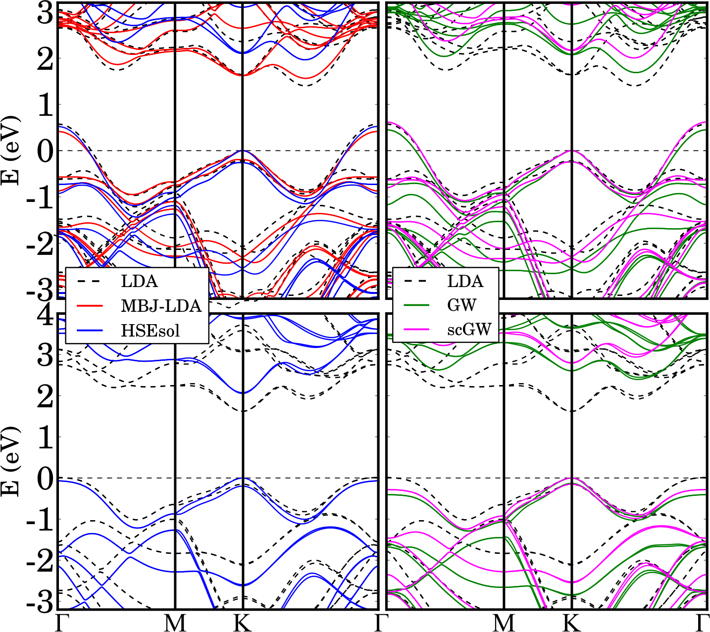
When comparing the numbers given in Table 6, LDA and PBEsol underestimate the transition (indirect gap of 0.85 eV) are found to be in agreement with previous calculations [142, 141]. Compared to LDA, the inclusion of local exchange as provided by the MBJ potential mainly affects the and energies resulting in a larger indirect gap of 1.15 eV. However, the band dispersion along towards is reduced resulting in almost energetically balanced CBEs at and , i. e., is only 60 meV. Therefore the difference between indirect and the direct gap is less pronounced than in LDA. Further improvement is achieved by taking into account non-local exchange using the HSEsol functional that increases the indirect as well as the direct gap. The difference in HSEsol is roughly 140 meV, significantly less compared to LDA ( 240 meV). Taking into account the dielectric screening in the approach strongly enhances the difference to 390 meV. This results in an indirect for bulk of 1.24 eV, in good agreement with experiment (1.2-1.3 eV) as well as previous calculations. [158, 140] The outstanding agreement of both, the indirect (1.24 eV) and direct (2.08eV) bulk gaps, with the values obtained by an all-electron code [158] verify the accuracy of the present PAW results.
A higher level of accuracy is reached by performing sc calculations. Compared to the band structure, the difference is again significantly reduced (to 160 meV), since is pushed up in energy almost back to the HSEsol position. The fundamental indirect sc gap is 1.39 eV and slightly overestimated compared to experiment, which is due neglecting the attractive electron-hole interactions via Vertex correction in . [88] In the – region, the sc band structure resembles the HSEsol, whereas we observe remarkable differences in the –– range. The and sc results are consistent to previous calculations [143] given in Tab. 6 within the uncertainties originating from computational aspects.
Single-layer is described as a semiconductor with a direct gap at on all levels of theory beyond standard DFT-LDA, provided that the crystal structure is fully relaxed as stressed in Sec. 2. Standard DFT (LDA and PBEsol) severely underestimates the direct gap of the single-layer structure. Besides that, LDA wrongly sets the VBM at at slightly higher energy than the VBE at . It is important to emphasize that the underestimated energy difference is observed if the single-layer slab is constructed from the optB86b-VdW relaxed bulk structure (in-plane lattice constant =3.164 Å), but not in case of the experimental bulk lattice constant =3.16 Å. Therefrom we conclude that the relative positions of the and energies are strongly dependent on the in-plane lattice constant. Hence is imperative the investigation of strain effects on the 1L- band structure presented later in this section.
Employing the HSEsol functional to 1L- shifts the conduction bands almost uniformly upwards in energy compared to DFT-LDA resulting in a rather constant , i. e., 360 meV and 300 meV, in HSEsol and LDA, respectively. Band dispersions in the valence band region are increased within the HSEsol description and the VBM splitting at is enhanced to 200 meV compared to the LDA value of 150 meV. The VBM at is stabilized by roughly 200 meV compared to in HSEsol calculations. Concerning approaches, the subtle changes of the band dispersions between and result in a significant change of the energy difference: stabilizes the CBM at by 130 meV, whereas sc enhances this energy difference by a factor of two. Note that the energy differences strongly depend on the total number of bands (NBANDS) included in the calculations (see Fig. 11) and the convergence with NBANDS itself is influenced by the amount of vacuum included in the single layer cell (20 Å in the present case). This means that using a larger amount of vacuum requires an increase of the NBANDS parameter as well. For this reason, the comparison between the present results and previously reported values, as summarized in Tab. 6, is difficult. The values listed in Tab. 6 refer to calculations with NBANDS=512. Increasing NBANDS from 512 to 1920 reduces the direct gap at by roughly 80 meV, the indirect gap by 60 meV, but the energy difference increases by 40 meV.
Analogous to bulk , including non-local exchange by HSEsol increases the gap (2.09 eV) considerably. The calculated quasiparticle gap amounts to 2.45 eV, which is smaller by 0.3-0.5 eV to reported values. [141, 140, 160] This difference is attributed to structural and computational details: A calculation performed with the experimental crystal structure and a reduced mesh of 882 yields 2.86 eV. Liang et al.reported a direct band gap of 1L- of 2.75 eV, [160] which was obtained by calculations taking into account a Coulomb interaction truncation to avoid spurious interlayer interaction between the periodically repeated monolayers, but using the generalized plasmon-pole model (GPP) for the dynamical screening and omitting SOC. The issues of the Coulomb interaction truncation, -point sampling, and vacuum layer thickness were also addressed by Hüser et al.[161], who argued that the band gap values converged with respect to -point sampling and slab distance are rougly 0.4 eV too small compared to the free standing monolayer (including Coulomb truncation). Once again this reflects the difficulty to achieve accurate results and explains the plethora of band gap data in literature.
Compared to the single-shot result for the direct gap, the sc further increases the gap to 2.72 eV in agreement with previously reported values as listed in Table 6. The slow convergence of the 1L- band gaps with the NBANDS parameter was only recently stressed [156] and might explain the larger values previously reported.
At this point it is important to recall that quasiparticle gaps are single-particle gaps. Their overestimation by roughly 0.5 eV compared to some experiment is explained by the missing electron-hole interactions (excitonic effects), which are strong in 2D materials due to confinement and lead to the formation of bound electron-hole pairs. These bound excitons reduce the direct band gap by their binding energy and define the optical gap, which is experimentally accessed by optical measurements such as photoluminescence or photoconductivity. Excitonic effects are addressed in the next section.
To conclude, it is evident based on the above discussion that the different levels of accuracy and/or complexity applied in the methods substantially alter the results. The non-local exchange and dynamical screening are inevitable for an accurate description of the electronic properties of . Based on our calculations of single-layer , a reasonable estimate for the direct band gap is 2.40.2eV and the spin-orbit splitting of the valence band edge at is 150-160 meV. The energy difference between the two valence band extrema in 1L- is much smaller than in bulk and very sensitive to the in-plane lattice constant. As put forward by Kuc and Heine[147], the estimations of the weak spin-orbit splitting of the conduction band edge is strongly dependent on the XC functional used in the DFT calculation and a better description by methods beyond ground state DFT is required. From our calculations, we deduce a conduction band splitting of 10 meV, which however falls within the estimated uncertainty range.
A final remark concerns the starting point of the calculations. One should keep in mind that the result can be influenced by the wave functions (orbitals) used for calculating and as pointed out in Ref. [162]. Thus, in the complexity of the method one can go a step forward by applying a full self-consistent procedure in the Green’s function and the screened interaction , consisting in the iterative solution of the Dyson equation. However, the extraordinarily cumbersome calculations required for this procedure restrict the application of this approach to small systems, such as binary molecules as N2 or CO [162]. Up to now this scheme has not been applied to single-layer and we think that its implementation for layered materials is still far.
4.4 Strain effects in single-layer
The ideal scenario of free-standing 2D layers as considered in most theoretical simulations is hardly fulfilled in reality. In the course of experiments or device fabrication with 2D materials, it is important to consider strain resulting e.g. from the lattice constant mismatch between the substrate and the 2D layer. Equally important in this context is the interaction of the 2D material with the substrate as shown in Ref. [148]. Therein, the ARPES scans of exfoliated single-layer compared to those of chemical vapor deposition grown single-layer on silicon revealed that the presence of substrate alone is sufficient to modify the band structure. In particular, the -substrate interactions are responsible for the pronounced flattening of the VBM at of on silicon.
In addition, recent experiments have demonstrated that application of tensile strain changes the gap from direct to indirect [30]. In particular, the flake deposited on a flexible substrate which is subsequently deformed in a controllable manner, experiences uniaxial tensile strain up to 2.2 %. The photoluminescence spectra of these samples show a clear transformation of the band character, and an associated reduction of the integrated intensity of the optical signal.
The sensitivity of TMDs band structure on the lattice constant opens the possibility to modify the band gap and thus the optical properties in a controlled way by external strain. This issue has been theoretically addressed either through LDA/GGA calculations [163, 27, 28, 31], or the method [144]. The effect of hydrostatic pressure on the vibrational, electronic, and optical properties of bulk, multi-, and single layer was investigated by Nayak et al.[33, 34] by combining various experiments (high resolution transmission electron microscopy, electrical resistance measurements, laser Raman spectroscopy, synchrotron X-ray diffraction experiments under high-pressure) with DFT calculations. Interestingly, while the direct bulk band gap decreases with increasing pressure, the direct band gap of 1L- increases by 11.7% up to 12 GPa before it is reduced. Thus the pressure induced electronic transition from the semiconducting to a semimetallic state occurs at much larger pressures in the latter. [34]
Being aware of the importance of substrate interactions, we investigated the strain effects on the electronic properties of 1L- within the approach and the model of free-standing 2D layers. Biaxial tensile strain has been realized by increasing the in-plane lattice constant of 1L-. The band structures of the strained materials were calculated with relaxed atomic positions and are shown in Fig. 15. The direct gap and interband transitions as a function of strain deduced from these band structures are collected in Tab. 7.
| strain (%) | +SOC | sc+SOC | ||||
|---|---|---|---|---|---|---|
| (eV) | (eV) | (eV) | ||||
| 0 | 2.51 | 2.71 | 0.08 | 2.76 | 2.85 | 0.39 |
| 1 | 2.37 | 2.44 | 0.24 | 2.61 | 2.58 | 0.55 |
| 2 | 2.23 | 2.18 | 0.41 | 2.47 | 2.31 | 0.72 |
| 3 | 2.11 | 1.93 | 0.55 | 2.34 | 2.06 | 0.86 |
| 4 | 1.98 | 1.69 | 0.69 | 2.21 | 1.82 | 0.99 |
With increasing in-plane lattice constant (biaxial tensile strain) the bond distances within the plane of the Mo-S-Mo sheets are changed, but also in the perpendicular direction through the relaxation along . According to Tab. 5, the valence states at (VBM) are mainly composed of S- and Mo- orbitals, whereas the valence states at have predominantly Mo character. Concerning the CBM at , the states are mainly Mo orbitals and the conduction band states around have predominantly Mo character. By changing the S-Mo-S bond lengths and angles due to tensile strain, the overlap of the Mo with the S is reduced, whereas the coupling between the Mo and S is increased.[32] As a consequence, the energy raises with respect to and the energy decreases compared to . Concomitantly, the gap decreases, but not as fast as the gap, which results in a transition to an indirect 1L- as illustrated in Fig. 16. Also evident in Fig. 16 is the linear dependence of the band gaps on biaxial tensile strain. +SOC suggests a transition strain of 1.6% (i. e., 3.21 Å), which is in good agreement with the value obtained by recent calculations (1.5%) [144]. Thus iterating the QP energies and one-electron wave functions in only, seems to change the linear decrease of the band gaps only marginally. The sc approach though, increases the direct gap rather constantly (by 0.2 eV) and significantly affects the band dispersions. The former results in a rigid shift of the direct gap dependence with strain, whereas the latter changes the and energy differences (compare data summarized in Tab. 7). Consequently, a much lower strain of 0.7% (i. e., 3.18 Å) for the direct-to-indirect transition in 1L- is obtained.
At this point, the present results are also compared to conclusions drawn from previous DFT-PBE calculations. Scalise et al.[27] proposed a stain-induced semiconductor to metal transition in 1L- on the basis of DFT-PBE calculations omitting SOC. When the slope of the linear fit to their band gap data as a function of biaxial tensile strain (Fig. 2(b) in Ref. [27]) is compared to that deduced from the present results, the obtained difference is roughly 30%., i. e., the DFT-PBE slope is 30% smaller. However, in both cases the closure of the indirect band gap with increasing tensile strain is estimated at (101)% tensile strain suggesting that the trend of the electronic properties as a function of strain is well reproduced by standard-DFT.
To compare with recent photoluminescence data [30], we also calculated the band structure of 1L- as a function of uniaxial tensile strain along the [100] direction with the approach.These results are summarized in Tab. 8. Since the electron-hole interaction is not included in the calculations at this stage, the experimental data have been rigidly shifted in energy for better comparison. Thereby it is assumed that the band gap renormalization due to excitonic effects does not change for small strains as applied in this case.
| strain (%) | +SOC | sc+SOC | ||||
|---|---|---|---|---|---|---|
| (eV) | (eV) | (eV) | ||||
| 0 | 2.51 | 2.71 | 0.08 | 2.85 | 2.76 | 0.39 |
| 1 | 2.43 | 2.56 | 0.19 | 2.58 | 2.56 | 0.53 |
| 2 | 2.37 | 2.44 | 0.27 | 2.47 | 2.49 | 0.60 |
| 3 | 2.29 | 2.31 | 0.36 | 2.33 | 2.42 | 0.69 |
| 4 | 2.21 | 2.17 | 0.46 | 2.20 | 2.35 | 0.77 |
The effect of the uniaxial strain on the band structure as shown in Fig. 15 is similar to that of biaxial strain. Again the energy decreases, whereas the energy increases with increasing uniaxial tensile strain giving rise to the direct-indirect gap transition, when becomes the VBM. Compared to biaxial strain, the slope of the linear dependence of the direct and indirect energy gaps is significantly smaller in the uniaxial case, i. e., roughly by a factor of two. As a consequence, the transition between direct and indirect single-layer occurs at a larger strain of 3.3% (equivalent to =3.26Å), which is roughly twice as high as in the biaxial case. Since the strain induced transition to an indirect gap significantly reduces the photoluminescence yield, understanding of the strain effects on the opto-electronic properties of single-layer is particularly relevant for technological applications.
4.5 Tight-binding modelling of single-layer MoS2
Tight-binding calculations can give further insight on the electronic properties of single-layer . The tight-binding method expands the wave functions in terms of an atomic orbital basis, thus giving a simple and intuitive physical picture of the electronic bands. The atomic orbital weight of each band state is directly accessible and changes in the band structure can be attributed to the change of a single tight-binding parameter.
Fig. 12 shows the change of the conduction and valence bands with variation of the atomic positions. However, it does not tell which orbitals are responsible for such variations. The parametrization given in Ref. [152] was used, but for clarity, we only consider -orbitals for Mo and -orbitals for S. Interatomic interactions up to the second nearest neighbors were taken into account. Figure 17 illustrates the band structure altering the hopping parameter while keeping fixed the remaining parameters. The subindices denote the kind of orbitals ( or ) and the symmetry of the bond, ,, and (see details in [164, 165]). The size of the red circles indicates the weight of the orbital and that of the blue circles the weight of the orbitals. We have increased each parameter %.

Focusing on nearest neighbor interaction between Mo-S, the parameters and carry the effect of a vertical displacement of the S atoms. In the ab initio calculations shown in Fig. 12 we have seen the total effect of the displacement on the band structure, but with the tight-binding formalism we can assign interactions to bands. The change in modifies the relative positions of the two local minima of the conduction band, and , producing almost a rigid shift of the valence band. In the case of the hopping parameter , the effect is rather different, giving a rigid shift of the conduction band at and . For the valence band, the dispersion at is strongly shifted to higher energies for % and to lower energies for % . The combination of these two weights is equivalent to displacing vertically the S atoms. In the case of the hopping parameters related with the orbitals of Mo atoms, the results are more complex. This can be seen for the cases of and in Fig. 17. Only for the case a minor influence on the band structure is obtained. The latter three parameters are also important in the change of the lattice parameter. The analysis in terms of the tight-binding model establishes the rather complex nature of covalent bonding formed by orbitals in TMDs. Note that a proper description of the conduction band would require a tight-binding model with more parameters to capture the interaction with farer neighbors and to enlarge the basis of atomic orbitals [166].
4.6 Effective charge carrier masses
Electron and hole carrier mobility is inversely proportional to their effective masses. The strain effects on effective mass are an important issue from the technological point of view. The effective electron and hole masses of bulk as a function of strain were studied on the DFT-HSE level by Peelaers and Van de Walle [123] and on DFT-LDA level by Scalise et al..[28] For the sake of completeness, the values for the bulk effective masses given in Ref. [123] are briefly summarized here. As pointed out in Ref. [143] and evident from Tab. III of Ref. [123], the valleys as well as edges at exhibit rather isotropic effective masses concerning both longitudinal and transversal directions. This justifies averaging over both directions as suggested in Ref. [141]. However, the longitudinal and transversal masses are quite different at the point (the same as in Ref. [123] and in Ref. [143]) and the point, which are the CBM and VBM in bulk , respectively. The value given in Ref. [123] for the transversal hole mass (i. e., [] in Ref. [123]) is 0.62, where is the electron rest mass. This number is in good agreement with the present result of 0.64, evaluated by a parabolic fit of the Wannier interpolated +SOC band structure, calculated with the experimental structure data according to in the direction (equal to ). For the optB86b-VdW relaxed bulk, we obtain 0.69 and 0.70 on the +SOC and sc+SOC level, respectively, indicating that the effective masses are well described on the +SOC level. The longitudinal hole mass given in Ref. [123] is 0.80 reflecting the anisotropy between transveral and longitudinal hole masses. The corresponding estimate from the +SOC band structure of the optB86b-VdW relaxed bulk is 1.05 and 1.03 for the experimental bulk structure. This 20% overestimation can be explained by the neglect of the spin-orbit interaction in the DFT-HSE calculations of Ref. [123].
The value given in Ref. [123] for the transversal electron mass (i. e., [] in Ref. [123]) is 0.53 that is close to the present calculations, which yield 0.58 at (through fitting of along or ). When evaluating the effective masses for both, electron and hole, at the point, their longitudinal and transversal component are strongly isotropic. On the +SOC level, an average hole mass of 0.40 and an average electron mass of 0.63 is obtained. Performing +SOC (sc+SOC) calculations with the optB86b-VdW optimized bulk structure yields = 0.39 ( = 0.40) and = 0.52 ( = 0.52), for the average hole and electron masses, respectively. For comparison, the corresponding values reported in Ref. [123] are 0.45 and 0.46 for and , respectively. Despite the different theoretical approaches, i. e., DFT with the HSE functional omitting spin-orbit coupling in Ref. [123] compared to calculations including SOC in the present work, the overall agreement between the results is good.
In the following, we focus on single-layer and present the effective electron and hole masses at the point for the longitudinal and transversal directions in Tab. 9. For comparison with available literature data, the average of the longitudinal and transversal component of the electron () as well as hole mass () are included too. Note that both, and sc calculations were performed with the optB86b-VdW optimized in-plane lattice constant and LDA-relaxed atomic positions. The values corresponding to the single-layer constructed from the experimental bulk structure are given for comparison in brackets in Tab. 9. As emphasized by Shi et al. [144], the effective masses are sensitive to strain (i. e., the in-plane lattice constant), spin-orbit interaction, the accuracy as well as the convergence criteria of the calculations, in particular the point sampling. It is difficult to disentangle these dependencies and the values summarized in Tab. 9 exhibit some spread. However they are consistent within the order of magnitude. The average values obtained in the present work for the effective electron mass range from 0.35-0.40, whereas average effective hole masses between 0.43 and 0.49 have been estimated.
In contrast to the electron masses, the anisotropy between longitudinal and transversal hole masses is strongly pronounced, thus yielding a larger uncertainty range for the average value. This may be explained by the significance of spin-orbit interactions: SOC affects the valence band dispersion at more strongly than the CBM [144]. A common observation is, that the electron mass is slightly smaller than the effective hole mass. As shown in the previous section, tensile strain shifts the valence band maximum to the point. At this point the band dispersion is significantly smaller than at the point resulting in much larger effective hole masses (2-3 estimated at 2% biaxial tensile strain) and therefore decreased hole mobilities.
| Single-layer | electron | hole | ||||
|---|---|---|---|---|---|---|
| () | () | () | () | |||
| +SOC | 0.33 | 0.36 | 0.35 | 0.40 | 0.50 | 0.45 |
| [0.36] | [0.36] | [0.36] | [0.35] | [0.50] | [0.43] | |
| +SOC [141] | [0.60] | [0.54] | ||||
| HSE [123] | [0.37] | [0.38] | [0.38] | [0.44] | [0.48] | [0.46] |
| +SOC [156] | 0.37 | 0.21 | ||||
| sc+SOC | 0.39 | 0.42 | 0.40 | 0.42 | 0.56 | 0.49 |
| [0.33] | [0.36] | [0.35] | [0.38] | [0.50] | [0.44] | |
| sc+SOC [143] | [0.34] | [0.35] | [0.35] | [0.46] | [0.43] | [0.44] |
| sc [144] | 0.36 | 0.39 | ||||
| sc [144] | [0.32] | [0.37] | ||||
5 Optical properties
In semiconductors like , electron-hole pairs interact via Coulomb attraction, forming excitons. Excitonic effects determine the optical properties of [167, 168, 169, 11, 10]. For example, experiments like photoluminescence [25, 170] and second harmonic generation [42, 43] are strongly influenced by excitonic effects. The most common excitonic effects are a red-shift in the optical gap (with respect to the quasiparticle gap) and, in some cases, a radical change in the optical spectra shape with respect to the independent particle spectra. This is in particularly the case when bound excitons (absorption peaks below the onset of the continuum) are formed. It has been shown before for hexagonal boron nitride (a prototypical wide-band gap layered material), that the anisotropic dielectric constant and the layered, quasi 2D confinement of excitons, leads to very strongly bound excitons[171, 149, 172]. Also in , there is a series of strongly bound excitons [140, 173, 145, 156](albeit with comparatively lower binding energies). Their binding energy depends on the number of layers (and the inter-layer distance in the case of a periodic supercell calculation for single-layers). These excitons determine the shape of the optical absorption spectra as will be explained in this section.
We analyze the optical properties of multi-layers in the framework of the Bethe-Salpeter equation. In addition, we compare single-layer optical properties with other transition metal dichalcogenides. Finally, we discuss results obtained applying empirical model Hamiltonians [174].
5.1 Bethe-Salpeter equation formalism
The Bethe-Salpeter equation (BSE) formalism gives an accurate description of the electron-hole interaction [175]. BSE is based on many-body perturbation theory [176]. Starting from the eigenvalues and wave functions of the system, obtained by ab initio methods, BSE gives the dielectric function and the excitonic binding energy without introducing any additional parameter [177, 178, 176, 175, 179]. BSE can be written as:
| (15) |
The electronic excitations are expressed in the basis of electron-hole pairs, . We assume vertical excitations at , from a valence-band state with quasiparticle energy , to a conduction-band state with energy . denote the expansion coefficients of the excitons and is the exciton energy. The interaction kernel describes the screened Coulomb and the exchange interaction between electrons and holes, which includes local field effects [175, 179]. In absence of electron-hole interaction . In this review, we consider only interband transitions. This is consistent with the experimental data, where the energy of optical excitations is always above the band gap value. Another important physical aspect is the omission of phonon-mediated transitions. They are important in indirect semiconductors, especially in the study of photoluminescence [180]. We focus mainly on the optical absorption spectra, where the weight of direct transitions is much higher than indirect transitions.
The exciton wave function, expressed in the basis of the electron-hole pairs
| (16) |
is a function of six coordinates, where and are the spatial coordinates of electron and hole. are the Kohm-Sham orbitals. We can define useful magnitudes from the exciton wave function. The weight of a transition is defined as the sum over all
| (17) |
Analogously, we define the weight of each , by summing over all transitions:
| (18) |
The amplitude of electron-hole pairs that compose each exciton, as a function of the transition energy is
| (19) |
Finally, the optical absorption spectrum is the imaginary part of the dielectric function, , written as
| (20) |
where are the dipole matrix elements of the transitions . The vector represents the light polarization. We restrict to light linearly polarized in the basal plane. The polarization perpendicular to the basal plane of MoS2 has a negligible contribution to absorption for energies close to the band gap.
Realistic results are only possible by performing an adequate convergence. In BSE calculations, we have to check carefully the number of valence and conduction bands, as well the -point mesh. Coarse -grids tend to overestimate the exciton binding energy. The building blocks of the BSE kernel, , are the screened Coulomb and the exchange interaction. Therefore, the dielectric function which enters in the Coulomb interaction has also to be converged with the number of bands and the -point grid (see Refs. [179, 181] for details).
The supercell geometry is also an important factor in BSE calculations. The long-range Coulomb interaction between replicas decreases slowly with distance. Consequently, GW and BSE corrections converge also slowly with the separation between replicas [149, 182]. In general, these corrections have opposite sign and partially cancel each other, and the total correction of the band gap is close to the experimental value. However, exact determination of the exciton binding energy requires overcoming this problem. An efficient technique is truncating the Coulomb potential (or Coulomb cut-off), simulating an infinite distance between replicas [183]. In single-layer , both GW band gap and exciton binding energy increases notably altough not their difference. A drawback of the Coulomb cut-off technique is the slower convergence with respect to the -point grid [161].

Figure 18(a) shows a typical BSE calculation for single-layer . Absoprtion is depicted with and without excitonic effects (solid and dashed black curves). Electron-hole interaction down-shifts the absorption threshold and increases the absorption coefficient. Amplitude functions and show the typical profile of an exciton built from a transition between nearly parabolic bands. Contribution decays for increasing energy, with the maximum close to the band edges. Panel (b) of Figure 18 represents the weight of the exciton (for exciton we obtain a similar result). The contribution is localized at and the -grid must be fine enough to describe accurately excitons and [145, 156]. The distribution of the weight reflects the importance of a proper convergence of the -grid to obtain realistic calculations.
In the following, we discuss the calculations of Ref. [145]. The -grids are (for single- and double-layer), and for bulk. We have included the bands in the energy window from -3 to 3 eV.
Figure 19 shows the optical absorption for single-layer, double-layer and bulk (solid lines). For comparison, we have included the independent-particle absorption spectra, without the electron-hole interaction, obtained in the random-phase approximation (RPA, dashed lines). The starting point of BSE is the GW eigenvalues and the LDA wave functions. We have drawn the experimental optical absorption (dots). We have rigidly shifted the theoretical spectra to match with the experimental points. The discrepancy is around 0.2 eV, within the error margin of GW and BSE calculations. Nonetheless, BSE describes well the main trends of the spectra. We remark the agreement in the absorption threshold, where BSE spectra reproduce accurately the spin-orbit splitting. The theoretical absorption at high energies also matches with the experiments. These high-energy peaks come from transitions located around the point.
We can also make a comparative analysis of single-layer, double-layer and bulk . The spectra have the same line-shape at the absorption threshold, two peaks that correspond to excitons and , followed by a plateau. The differences arise from the exciton binding energy, which decreases with the number of layers. The reason of such decreasing is related to a larger dielectric screening in double-layer and bulk. The high-energy exciton exhibits a sharp peak in the case of single-layer MoS2, and it becomes difficult to distinguish in double-layer and bulk. Experimental observation confirms the latter result, in which we observe a broad absorption for bulk MoS2, in contrast to the relatively narrow peak of single-layer . Putting together the theoretical and experimental data we can deduce that the interlayer interaction affects mainly exciton and . This conclusion agrees with the study of MoS2/WS2 heterostructures of Ref. [173]: the optical spectra of MoS2/WS2 is the addition of the spectra of independent single-layers of MoS2 and WS2, and not the combination of spectra modified by a strong interlayer coupling. Inspecting the exciton wave functions we can get a better insight into the interlayer coupling.
The intensity of the excitonic peaks is directly related to the spatial localization of the wave function. Figure 20 shows the exciton wave functions for the excitons (a) and (b) for the case of single-layer . We have placed the hole at the Mo atom. This makes sense as the valence band states at are composed primarily by Mo -orbitals (see Table 5). The exciton is extended more than 50 Å, in consonance with the localization at the momentum space (see Fig. 18). Exciton has an identical wave function (not shown here). On the contrary, the high-energy exciton is localized in a few unit cells, in less that 30 Å. The exciton is built from a contribution of a larger set of points than in the case of . We will discuss the features of this exciton below.
By looking at the exciton wave function in a plane parallel to the vertical axis we can learn more details about the interlayer coupling. Figures 20(c) and (d) show the lateral view of the exciton in single-layer and bulk, respectively. The exciton density lies mainly on the Mo atoms for the single-layer and only a tiny fraction is outside the layer. Bulk does not exhibit big differences with respect to the single-layer. Therefore, excitons and remain in one layer, without coupling between layers, and optical transitions take place at the same layer. In other layered materials like hexagonal boron nitride, we find that excitons can spread over several layers [184].

Another distinctive optical property of single-layer is the exciton , visualized by a sharp peak at high energy (2.75 eV). Is this peak built from a single exciton or do we see the collective effect of many excitons? Figure 21 (a) shows the excitonic peak , together with each contribution (vertical lines). On the right side we have drawn the profile of the corresponding exciton wave function. Figure 21 (b) depicts the weigth of the first vertical line (in red). The characteristics of this exciton are radically different from the case of and excitons. First, the exciton is localized around in the space, forming a kind of hexagonal wheel. Second, defining the binding energy is ambiguous. We know that for bound excitons, like and , the binding energy is defined as the difference between exciton energy and the band gap energy. The transition energies of the exciton fall within the continuous of states, making difficult to define such binding energy. Third, the sharp peak is the collective contribution of several excitons with similar energy and wave function, as we can see from the wave functions of Fig. 21 (b). The parallel transitions lead to a singularity in the density of states, and often the term Van-Hove exciton is used to denominate such peak [185, 186, 187].
Recently, several experiments have found fingerprints of the Van-Hove exciton, e.g., two-photon spectroscopy [43], photocurrent spectroscopy [188], and light scattering spectra [189]. Some properties of the Van Hove exciton, under discussion nowadays, are the large electric field required to dissociate the exciton, and the spontaneous decay of Van Hove excitons into a free electron-hole pair.
Additionally, single-layer exhibits a Rydberg-like exciton series in the optical spectra [156]. To capture these excited states the convergence of the -grid requires up to . In comparison with the Rydberg series for a 2D hydrogen model, the excitation spectrum of single-layer is completely different (see in supplementary material of Ref. [156]). The reason for this difference is the spatial variation of the dielectric function in . The Rydberg-like series and its particular behaviour has been also observed in single-layer WS2 [190].
5.2 Optical spectra of other transition metal dichalcogenides
The rest of semiconductor transition metal dichalcogenides, MoSe2, WS2, and WSe2, shares the interesting optical properties of . They have similar lattice parameters, band gap and spin-orbit splitting [191, 190, 39, 192, 193]. However, band gaps are different enough to generate band mismatch in heterostructures. We can combine TMDs in vertical heterostructures for quantum well growth [49, 173, 194], with the purpose of selective confinement of photogenerated excitons.
| WS2 | WSe2 | MoSe2 | |
|---|---|---|---|
| (Ang.) | 3.127 | 3.250 | 3.253 |
| (eV) | 1.739 | 1.458 | 1.516 |
| (meV) | 406.8 | 457.2 | 185.6 |
Figure 22 shows the BSE spectra of single-layer MoSe2, WS2, and WSe2 (solid lines) and the RPA spectra (dashed lines). We have included experimental data for WS2, and WSe2. On the right side we present a lateral view of the exciton wave functions. Starting points are the LDA calculations, including spin-orbit. We have used a -grid and we have included four valence and conduction bands. The static dielectric function is obtained with 60 bands. More accurate spectra require using self-consistent GW quasiparticle eigenvalues, as shown in Section 4. For introductory purposes, using LDA as starting point allows to describe the main physics of the optical properties of TMDs.
All the spectra exhibit two well differentiated excitons, and , which come from transitions centered at the point, analogously to single-layer . The spin-orbit splitting determines the separation between the peaks and . The theoretical splitting agrees very well with the experiments. Exciton is uniquely composed of the top of the valence band and the bottom of the conduction band. Accordingly, exciton is mostly composed by the second valence band () and the conduction band with opposite spin. In comparison with the exciton of single-layer , we observe a similar spreading of the wave functions for the other TMDs. Evidently, the spin-orbit splitting is much higher in compounds which include tungsten. In valley-physics, this has important consequences. The tuning of the excitation energy is crucial to obtain an excitonic population with certain polarization. Tuning in WS2 and WSe2 will in principle be easier due to the energy separation and the generation of a valley polarization will be more efficient. We will comment on this again in subsection 5.5, devoted to valley physics.
The high-energy excitons (from to ) show a strong spatial confinement, analogously to . However, they split in several and well differentiated peaks. Spin-orbit also splits the bands around , and this results in the splitting of the excitons. The experimental spectra of WSe2 agree with the calculation in the relative separation between the and peaks. This latter compound presents the strongest spin-orbit coupling effects, either for the bound excitons and , or the Van-Hove exctions s. In summary, selenium-based TMDs have an -peak separation close to 0.5 eV and sulphur-based TMDs have a difference below 0.2 eV.
5.3 Empirical models for excitons in
Analytical approaches are very useful in the study of excitons in single-layer and they can be easily expanded to explore excitonic complexes such as trions and biexcitons [40]. These approaches are also suitable to obtain the Rydberg excitonic series [190].
The tight-binding ansatz of the electronic wave function takes the orbital composition of the valence and conduction band states obtained from DFT results. Using the density matrix formalism, one obtains the analytical solution of the band structure close to the points and [174].
where is the valley and denotes band and spin. Momentum dependence is given by
The Taylor expansion simplifies the eigenvalue momentum dependence to a parabolic band structure
and the solution of the model Hamiltonian gives the eigenvectors, from which one can obtain the carrier-light matrix elements. Transitions at and are between Mo- orbitals of the valence band and S- orbitals of the conduction band. These transitions can be optically excited by circularly polarized light. The right-handed circularly polarized light will excite states at and the left-handed light at , allowing a valley selection. This is the cornerstone of valley physics, which will be presented in subsection 5.5. Figure 23 shows the results of Ref. [174] for the matrix elements and the absorption spectra for negative (a,c) and positive (b,d) light polarization. Fig. 23(e) shows our own calculations of the optical matrix elements for linear polarization. In the latter case we excite the valleys and with the same probability. Agreement between DFT and the model Hamiltonian is excellent and justifies the use of the analytical approach.
Excitonic effects are included introducing the Coulomb interaction into the model Hamiltonian [174]. In the framework of the semiconductor Bloch equation, from microscopic polarization, one can obtain an analytical expression of the absorption coefficient (for a complete derivation, see Ref. [196]). In addition, the effects of the substrate on the exciton binding energy can be quantified by a proper choice of the dielectric constant.
The application of the model shows a binding energy of the exciton for free-standing single-layer of 860 meV. The binding energy decreases to 455 meV on top of a silicon oxide substrate. Among limitations of this analytical approch are the calculation of the relative intensity of the and peaks, which can be attributed to higher-order effects beyond the Hartree-Fock approximation. The prediciton of the high-energy excitons will also require a much more complicated reformulation of the model.

5.4 Experimental determination of the band gap and exciton binding energy in MoSe2
The experimental determination of electronic band gap and exciton binding energy requires at least two techniques for determining univoquely these magnitudes. We have seen that the electronic band gap is related to the single-particle excitation. In addition, the binding energy is the difference between the electronic and the optical band gap. In Ref. [197], Ugeda et. al. have used a combination of experiments and theory to give an accurate value for the binding energy of single-layer MoSe2. The measurements by scanning tunneling spectroscopy (STS) have measured the electronic gap, and photoluminescence (PL) has defined the optical gap. The reported values are eV (electronic band gap) and eV, what gives a binding energy of . Experimental findings are well supported by GW and BSE calculations, taking into account the incidence of the substrate (bilayer graphene). As mentioned, the substrate increases the dielectric constant and reduces the electronic and optical band gaps. However, a full GW and BSE calculation of the system MoSe2 plus substrate would be computationally very complex. Alternatively, authors have made apart the calculation of the substrate dielectric screening. The MoSe2 contribution is obtained in the random phase approximation, including local fields. Afterwards, the MoSe2 and substrate contributions are merged in the Bethe-Salpeter equation. The binding energy reduces from a value of 0.65 eV to 0.52 eV, with an uncertainty of 0.10 eV, in fair agreement with experimental values. Therefore, a wise treatment of substrate influence on electronic and optical properties appears as an important aspect in calculations aiming of having predictive character.
5.5 Spin-orbit interaction and valley physics in MoS2
The lack of inversion symmetry and the strong spin-orbit interaction in single-layer lead to what is called valley-physics. The valley index denotes the momentum of the valence band state, or , and the spin (up or down). As shown above, excitons and can be generated exclusively from the valley or by selecting the appropiate light polarization. Among the potential uses and research related with this new concept are information transport by means of a new carrier, defined in terms of the valley index, or the generation of a valley-Hall effect [38, 36, 37, 198].

In the case of single-layer , spin-orbit coupling splits the valence band maximum at and by meV. Moreover, the point group symmetry does not have inversion symmetry. Under these conditions, Kramer’s degeneracy states that . In the case of the valence band states at , we find the relation . The spin of the valence band states and flips under change of inequivalent points. In other words, valence band edge valley and spin are coupled. Figure 24(a) illustrates the spin composition of the valence band edges at and . The spin-orbit splitting is negligible (a few ) for conduction states and we can consider a two-fold degenerate state. Following Ref. [35], we can assign the following total angular momenta, , in the -direction to the conduction and valence band states. The conduction band state at is energy degenerate with and . In the case of valence band states, and have and respectively, split in energy by meV. The values for the total angular momentum of the valence and conduction states at are obtained by multiplying the ones at by .
Exposing the crystal to circularly polarized light of momentum will promote a valence electron with momentum to the conduction state of , or from the valence state to the conduction state , both transitions taking place in the valley . These transitions are consequently forbidden at valley . By tuning the excitation energy one can precisely select which couple of valence-conduction band states are participating and from which valley. Thus, light with the energy of the band gap and momentum will only promote valence electrons with . In this way, one can create a stable population of electron-hole pairs with defined valley index. In other words, a “valley polarization” is generated. This has been demonstrated theoretically and experimentally in Refs. [38, 36, 35]. The persistence of this valley polarization is related to the conservation of spin. Hence, the flipping of valley index implies a spin flip, which is only possible by scattering with magnetic impurities or by means of relaxation via intra- and inter-valley scattering [35, 199].
Nowadays, the selective generation of valley polarizations is presented as a way to develop the so-called valleytronics and the stability of the valley polarization is being investigated. Techniques such as ultra-fast spectroscopy make it possible to trace the time evolution of valley polarization. Although theory predicts a long lifetime for the valley polarization, recent studies observe a non-negligible decoherence [200], which points towards other reasons than magnetic impurities as the origin of the spin-flip. Experimental studies have been undertaken to identify the reasons of decoherence of valley polarizations [201, 170, 202, 203, 199]. The analysis of the time-dependent optical response of single-layer supported in several substrates or suspended in vacuum can give a hint [170] of how the environment can alter the electronic structure and hence the valley polarization. Other causes of decoherence can be the interplay between intra-valley and inter-valley scattering. Here the detuning of the valley polarization can take place via intermediate transitions through the point [199]. The proliferation of experimental results using time-dependent spectroscopy is increasing our knowledge of the electronic and optical properties of and other two-dimensional materials.
6 Conclusions
This review has summarized the theoretical and computational description of the fundamental spectroscopic properties of in its single-layer, few-layer, and bulk form. We have focussed on but many of the findings are similarly valid for the other semiconducting transition-metal dichalcogenides (TMDs) of 2H polytype. We have summarized the numerous published investigations that report partly controversial findings. We have analysed the possible reasons for the discrepancies by performing comprehensive density functional theory calculations on different levels of approximation. For the geometry, we have investigated the inclusion of Van der Waals interactions. For the quasiparticle gap, we have compared the results obtained by DFT with different hybrid functionals with the result obtained by many-body perturbation theory. Excitonic effects in the optical properties are described with the Bethe-Salpeter approach. Thereby, our review provides a general idea on the most important computational issues that arise when studying TMDs. We hope that it gives stimulation to the scientific community to achieve accurate and converged results.
The structural and vibrational properties are well described by density functional theory approaches including Van der Waals interactions. Excellent results are obtained for the lattice parameters and the calculated phonon frequencies that agree well with different experimental data from Raman spectroscopy and neutron scattering. In this context, the open question about the anomalous Davydov splitting has been explained in terms of many neighbors interaction between Mo-S atoms of different layers. The anomalous trend of the mode as a function of layer number is a consequence of the renormalization of the atomic distances due to the free surface[62].
There is a variety of results in the literature for the band structures and band gaps based on different levels of computational approach. The spread of results is connected to the inherent problem of local and semilocal exchange correlation functionals to yield accurate band gaps and can be overcome by including nonlocal exchange (hybrid functionals) or using the approximation. The latter is commonly applied in a one-shot manner () on top of DFT wave functions. Different schemes of self-consistency lead to a large spread in the quasiparticle gaps. Reliable band structures and relative positions between the two lowest conduction band extrema and , but slightly overestimated band gaps, are obtained by self-consistent quasiparticle calculations provided that one starts from a fully optimized crystal structure. Particularly important in the case of single-layer is the convergence of the calculations with respect to the -point grid, the number of virtual states, and the vacuum layer in the slab approach.
As for most other layerd materials, excitonic effects are very pronounced in the optical properties of . The absorption spectra of mono-, bilayer, and bulk display three pronounced peaks. The excitons are calculated with the Bethe-Salpeter equation based on the full spinorial wave functions in order to include the effects of spin-orbit interaction. In all single-layer, double-layer and bulk , there is a pronounced splitting between A and B excitons which can be traced back to the splitting of the valence band maximum at the high-symmetry point . For single-layer , the splitting is due to the strong spin-orbit splitting of the valence band maximum at , for for double-layer and bulk , the splitting is due to the interlayer interaction. Interestingly, the brightest exciton of single-layer is not found at the absorption threshold, but at higher energies (around 3 eV). This exciton, also called “Van Hove exciton” stems from a large joint density of states due to parallel conduction and valence bands around . It plays an important role in the resonant Raman spectroscopy of various semiconducing transition-metal dichalcogenides.
7 Acknowledgements
A. M.-S. and L.W. acknowledge support by the National Research Fund, Luxembourg (Projects C14/MS/773152/FAST-2DMAT and INTER/ANR/13/20/NANOTMD). Calculations were performed on the Vienna Scientific Cluster (VSC) and on the IDRIS supercomputing center, Orsay (Proj. No. 091827). We acknowledge stimulating discussions with D. Sangalli and A. Marini. We thank E. Kalesaki, S. Reichardt and H.P.C. Miranda for critically reading the manuscript.
and E. Kalesaki for critically reading the manuscript.
References
- [1] K. S. Novoselov, D. Jiang, F. Schedin, T. J. Booth, V. V. Khotkevich, S. V. Morozov, and A. K. Geim. Proceedings of the National Academy of Sciences of the United States of America 102, 30, 10451 (2005).
- [2] J. Wilson and A. Yoffe. Advances in Physics 18, 73, 193 (1969).
- [3] S. Jiang, M. Q. Arguilla, N. D. Cultrara, and J. E. Goldberger. Accounts of Chemical Research 48, 1, 144 (2015). PMID: 25490074.
- [4] K. S. Novoselov, A. K. Geim, S. V. Morozov, D. Jiang, Y. Zhang, S. V. Dubonos, I. V. Grigorieva, and A. A. Firsov. Science 306, 5696, 666 (2004).
- [5] A. K. Geim. Science 324, 5934, 1530 (2009).
- [6] M. I. Katsnelson, K. S. Novoselov, and A. K. Geim. Nat Phys 2, 9, 620 (2006).
- [7] M. I. Katsnelson. Graphene: Carbon in Two Dimensions. Cambridge University Press (2012).
- [8] D. Lembke, S. Bertolazzi, and A. Kis. Accounts of Chemical Research 48, 1, 100 (2015). PMID: 25555202.
- [9] RadisavljevicB., RadenovicA., BrivioJ., GiacomettiV., and KisA. Nat Nano 6, 3, 147 (2011).
- [10] K. F. Mak, C. Lee, J. Hone, J. Shan, and T. F. Heinz. Phys. Rev. Lett. 105, 136805 (2010).
- [11] A. Splendiani, L. Sun, Y. Zhang, T. Li, J. Kim, C.-Y. Chim, G. Galli, and F. Wang. Nano Letters 10, 4, 1271 (2010). PMID: 20229981.
- [12] D. Lembke and A. Kis. ACS Nano 6, 11, 10070 (2012).
- [13] B. W. H. Baugher, H. O. H. Churchill, Y. Yang, and P. Jarillo-Herrero. Nano Letters 13, 9, 4212 (2013).
- [14] B. Radisavljevic, M. B. Whitwick, and A. Kis. ACS Nano 5, 12, 9934 (2011).
- [15] Y. Zhang, J. Ye, Y. Matsuhashi, and Y. Iwasa. Nano Letters 12, 3, 1136 (2012).
- [16] O. Lopez-Sanchez, D. Lembke, M. Kayci, A. Radenovic, and A. Kis. Nat Nano 8, 7, 497 (2013).
- [17] Y. Zhang, H. Li, L. Wang, H. Wang, X. Xie, S.-L. Zhang, R. Liu, and Z.-J. Qiu. Sci. Rep. 5, 7938, 07938 (2015).
- [18] M. Fontana, T. Deppe, A. K. Boyd, M. Rinzan, A. Y. Liu, M. Paranjape, and P. Barbara. Sci. Rep. 3, (2013).
- [19] M. M. Furchi, A. Pospischil, F. Libisch, J. Burgdörfer, and T. Mueller. Nano Letters 14, 8, 4785 (2014). PMID: 25057817.
- [20] A. Pospischil, M. M. Furchi, and T. Mueller. Nature Nanotechnology 9, 4, 257–261 (2014).
- [21] H. R. Gutiérrez, N. Perea-López, A. L. Elías, A. Berkdemir, B. Wang, R. Lv, F. López-Urías, V. H. Crespi, H. Terrones, and M. Terrones. Nano Letters 13, 8, 3447 (2013).
- [22] H. Li, Z. Yin, Q. He, H. Li, X. Huang, G. Lu, D. W. H. Fam, A. I. Y. Tok, Q. Zhang, and H. Zhang. Small 8, 1, 63 (2012).
- [23] A. Castellanos-Gomez, M. Barkelid, A. Goossens, V. E. Calado, H. S. van der Zant, and G. A. Steele. Nano letters 12, 6, 3187 (2012).
- [24] J. N. Coleman, M. Lotya, A. O’Neill, S. D. Bergin, P. J. King, U. Khan, K. Young, A. Gaucher, S. De, R. J. Smith, I. V. Shvets, S. K. Arora, G. Stanton, H.-Y. Kim, K. Lee, G. T. Kim, G. S. Duesberg, T. Hallam, J. J. Boland, J. J. Wang, J. F. Donegan, J. C. Grunlan, G. Moriarty, A. Shmeliov, R. J. Nicholls, J. M. Perkins, E. M. Grieveson, K. Theuwissen, D. W. McComb, P. D. Nellist, and V. Nicolosi. Science 331, 6017, 568 (2011).
- [25] T. Korn, S. Heydrich, M. Hirmer, J. Schmutzler, and C. Schuller. Applied Physics Letters 99, 10, 102109 (2011).
- [26] R. S. Sundaram, M. Engel, A. Lombardo, R. Krupke, A. C. Ferrari, P. Avouris, and M. Steiner. Nano Letters 13, 4, 1416 (2013).
- [27] E. Scalise, M. Houssa, G. Pourtois, V. Afanas’ev, and A. Stesmans. Nano Research 5, 1, 43 (2012).
- [28] E. Scalise, M. Houssa, G. Pourtois, V. Afanas’ev, and A. Stesmans. Physica E: Low-dimensional Systems and Nanostructures 56, 0, 416 (2014).
- [29] K. He, C. Poole, K. F. Mak, and J. Shan. Nano Letters 13, 6, 2931 (2013).
- [30] H. J. Conley, B. Wang, J. I. Ziegler, R. F. Haglund, S. T. Pantelides, and K. I. Bolotin. Nano Letters 13, 8, 3626 (2013).
- [31] L. Dong, R. Namburu, T. O’Regan, M. Dubey, and A. Dongare. Journal of Materials Science 49, 19, 6762 (2014).
- [32] D. M. Guzman and A. Strachan. Journal of Applied Physics 115, 24, 243701 (2014).
- [33] A. P. Nayak, S. Bhattacharyya, J. Zhu, J. Liu, X. Wu, T. Pandey, C. Jin, A. K. Singh, D. Akinwande, and J.-F. Lin. Nature Communications 5, 3731 (2014).
- [34] A. P. Nayak, T. Pandey, D. Voiry, J. Liu, S. T. Moran, A. Sharma, C. Tan, C.-H. Chen, L.-J. Li, M. Chhowalla, J.-F. Lin, A. K. Singh, and D. Akinwande. Nano Letters 15, 1, 346 (2015). PMID: 25486455.
- [35] D. Xiao, G.-B. Liu, W. Feng, X. Xu, and W. Yao. Phys. Rev. Lett. 108, 196802 (2012).
- [36] K. F. Mak, K. He, J. Shan, and T. F. Heinz. Nat Nano 7, 8, 494 (2012).
- [37] H. Zeng, J. Dai, W. Yao, D. Xiao, and X. Cui. Nat Nano 7, 8, 490 (2012).
- [38] T. Cao, G. Wang, W. Han, H. Ye, C. Zhu, J. Shi, Q. Niu, P. Tan, E. Wang, B. Liu, and J. Feng. Nat Commun 3, 887 (2012).
- [39] N. Kumar, J. He, D. He, Y. Wang, and H. Zhao. Nanoscale pages – (2014).
- [40] K. F. Mak, K. He, C. Lee, G. H. Lee, J. Hone, T. F. Heinz, and J. Shan. Nat Mater 12, 3, 207 (2013).
- [41] G. Plechinger, P. Nagler, J. Kraus, N. Paradiso, C. Strunk, C. Schüller, and T. Korn. physica status solidi (RRL) – Rapid Research Letters 9, 8, 457 (2015).
- [42] N. Kumar, S. Najmaei, Q. Cui, F. Ceballos, P. M. Ajayan, J. Lou, and H. Zhao. Phys. Rev. B 87, 161403 (2013).
- [43] L. M. Malard, T. V. Alencar, A. P. M. Barboza, K. F. Mak, and A. M. de Paula. Phys. Rev. B 87, 201401 (2013).
- [44] B. W. H. Baugher, H. O. H. Churchill, Y. Yang, and P. Jarillo-Herrero. Nature Nanotechnology 9, 4, 262–267 (2014).
- [45] J. S. Ross, P. Klement, A. M. Jones, N. J. Ghimire, J. Yan, D. G. Mandrus, T. Taniguchi, K. Watanabe, K. Kitamura, W. Yao, D. H. Cobden, and X. Xu. Nature Nanotechnology 9, 4, 268–272 (2014).
- [46] A. K. Geim and I. V. Grigorieva. Nature 499, 7459, 419 (2013).
- [47] C. Huang, S. Wu, A. M. Sanchez, J. J. P. Peters, R. Beanland, J. S. Ross, P. Rivera, W. Yao, D. H. Cobden, and X. Xu. Nat. Mater. 13, 1096 (2014).
- [48] Y. Gong, J. Lin, X. Wang, G. Shi, S. Lei, Z. Lin, X. Zou, G. Ye, R. Vajtai, B. I. Yakobson, H. Terrones, M. Terrones, B. Tay, J. Lou, S. T. Pantelides, Z. Liu, W. Zhou, and P. M. Ajayan. Nat. Mater. 13, 1135 (2014).
- [49] L. Britnell, R. M. Ribeiro, A. Eckmann, R. Jalil, B. D. Belle, A. Mishchenko, Y.-J. Kim, R. V. Gorbachev, T. Georgiou, S. V. Morozov, A. N. Grigorenko, A. K. Geim, C. Casiraghi, A. H. C. Neto, and K. S. Novoselov. Science 340, 6138, 1311 (2013).
- [50] J. He, K. Hummer, and C. Franchini. Phys. Rev. B 89, 075409 (2014).
- [51] L. Debbichi, O. Eriksson, and S. Lebègue. Phys. Rev. B 89, 205311 (2014).
- [52] K. Liu, L. Zhang, T. Cao, C. Jin, D. Qiu, Q. Zhou, A. Zettl, P. Yang, S. G. Louie, and F. Wang. Nat. Commun. 5, 4966 (2014).
- [53] J. L. Verble and T. J. Wieting. Phys. Rev. Lett. 25, 362 (1970).
- [54] T. J. Wieting and J. L. Verble. Phys. Rev. B 3, 4286 (1971).
- [55] N. Wakabayashi, H. G. Smith, and R. M. Nicklow. Phys. Rev. B 12, 659 (1975).
- [56] P. A. Bertrand. Phys. Rev. B 44, 5745 (1991).
- [57] C. Lee, H. Yan, L. E. Brus, T. F. Heinz, J. Hone, and S. Ryu. Acs Nano 4, 5, 2695 (2010).
- [58] B. Windom, W. Sawyer, and D. Hahn. Tribology Letters 42, 3, 301 (2011).
- [59] H. Li, Q. Zhang, C. C. R. Yap, B. K. Tay, T. H. T. Edwin, A. Olivier, and D. Baillargeat. Advanced Functional Materials 22, 7, 1385 (2012).
- [60] G. Plechinger, S. Heydrich, J. Eroms, D. Weiss, C. Schuller, and T. Korn. Applied Physics Letters 101, 10, 101906 (2012).
- [61] M. Boukhicha, M. Calandra, M.-A. Measson, O. Lancry, and A. Shukla. Phys. Rev. B 87, 195316 (2013).
- [62] X. Luo, Y. Zhao, J. Zhang, Q. Xiong, and S. Y. Quek. Phys. Rev. B 88, 075320 (2013).
- [63] Y. Zhao, X. Luo, H. Li, J. Zhang, P. T. Araujo, C. K. Gan, J. Wu, H. Zhang, S. Y. Quek, M. S. Dresselhaus, and Q. Xiong. Nano Letters 13, 3, 1007 (2013).
- [64] X. Zhang, W. P. Han, J. B. Wu, S. Milana, Y. Lu, Q. Q. Li, A. C. Ferrari, and P. H. Tan. Physical Review B 87, 11, 115413 (2013).
- [65] X. Zhang, X.-F. Qiao, W. Shi, J.-B. Wu, D.-S. Jiang, and P.-H. Tan. Chem. Soc. Rev. 44, 2757 (2015).
- [66] C. Ataca, H. Sahin, E. Akturk, and S. Ciraci. Journal of Physical Chemistry C 115, 10, 3934 (2011).
- [67] A. Molina-Sánchez and L. Wirtz. Phys. Rev. B 84, 155413 (2011).
- [68] H. Terrones, E. D. Corro, S. Feng, J. M. Poumirol, D. Rhodes, D. Smirnov, N. R. Pradhan, Z. Lin, M. A. T. Nguyen, A. L. Elias, T. E. Mallouk, L. Balicas, M. A. Pimenta, and M. Terrones. Sci. Rep. 4, 4215 (2014).
- [69] C. Rice, R. J. Young, R. Zan, U. Bangert, D. Wolverson, T. Georgiou, R. Jalil, and K. S. Novoselov. Physical Review B 87, 8, 081307 (2013).
- [70] R. Dickinson and L. Pauling. J. Am. Chem. Soc. 45, 1466 (1923).
- [71] B. Schönfeld, J. J. Huang, and S. C. Moss. Acta Cryst. B 39, 404 (1983).
- [72] A. A. Al-Hilli and B. L. Evans. J. Cryst. Growth 15, 93 (1972).
- [73] V. Petkov, S. J. L. Billinge, P. Larson, S. D. Mahanti, T. Vogt, K. K. Rangan, and M. G. Kanatzidis. Phys. Rev. B 65, 092105 (2002).
- [74] J. He, K. Hummer, and C. Franchini. submitted (2013).
- [75] L. Wirtz and A. Rubio. Solid State Communications 131, 3–4, 141 (2004).
- [76] G. Kern, G. Kresse, and J. Hafner. Phys. Rev. B 59, 8551 (1999).
- [77] J. Serrano, A. Bosak, R. Arenal, M. Krisch, K. Watanabe, T. Taniguchi, H. Kanda, A. Rubio, and L. Wirtz. Phys. Rev. Lett. 98, 095503 (2007).
- [78] A. Allard and L. Wirtz. Nano Letters 10, 11, 4335 (2010).
- [79] F. Fromm, M. H. Oliveira Jr, A. Molina-Sánchez, M. Hundhausen, J. M. J. Lopes, H. Riechert, L. Wirtz, and T. Seyller. New Journal of Physics 15, 4, 043031 (2013).
- [80] M. Endlich, A. Molina-Sánchez, L. Wirtz, and J. Kröger. Phys. Rev. B 88, 205403 (2013).
- [81] G. Kresse and J. Furthmüller. Comp. Mat. Science 6, 15 (1996).
- [82] G. Kresse and J. Furthmüller. Phys. Rev. B 54, 11169 (1996).
- [83] P. E. Blöchl. Phys. Rev. B 50, 17953 (1994).
- [84] G. Kresse and D. Joubert. Phys. Rev. B 59, 1758 (1999).
- [85] Y.-S. Kim, K. Hummer, and G. Kresse. Phys. Rev. B 80, 035203 (2009).
- [86] M. Shishkin and G. Kresse. Phys. Rev. B 74, 035101 (2006).
- [87] M. Shishkin and G. Kresse. Phys. Rev. B 75, 235102 (2007).
- [88] M. Shishkin, M. Marsman, and G. Kresse. Phys. Rev. Lett. 99, 246403 (2007).
- [89] D. M. Ceperley and B. J. Alder. Phys. Rev. Lett. 45, 566 (1980).
- [90] J. P. Perdew, A. Ruzsinszky, G. I. Csonka, O. A. Vydrov, G. E. Scuseria, L. A. Constantin, X. Zhou, and K. Burke. Phys. Rev. Lett. 100, 136406 (2008).
- [91] J. c. v. Klimeš, D. R. Bowler, and A. Michaelides. Phys. Rev. B 83, 195131 (2011).
- [92] M. Dion, H. Rydberg, E. Schrd̈er, D. C. Langreth, and B. I. Lundqvist. Phys. Rev. Lett. 92, 246401 (2004).
- [93] F. D. Murnaghan. Proc. Natl. Acad. Sci. USA 30, 244 (1944).
- [94] A. C. Ferrari, J. C. Meyer, V. Scardaci, C. Casiraghi, M. Lazzeri, F. Mauri, S. Piscanec, D. Jiang, K. S. Novoselov, S. Roth, and A. K. Geim. Phys. Rev. Lett. 97, 187401 (2006).
- [95] D. Graf, F. Molitor, K. Ensslin, C. Stampfer, A. Jungen, C. Hierold, and L. Wirtz. Nano Letters 7, 2, 238 (2007). PMID: 17297984.
- [96] S. Berciaud, S. Ryu, L. E. Brus, and T. F. Heinz. Nano Letters 9, 1, 346 (2009). PMID: 19099462.
- [97] F. Forster, A. Molina-Sanchez, S. Engels, A. Epping, K. Watanabe, T. Taniguchi, L. Wirtz, and C. Stampfer. Phys. Rev. B 88, 085419 (2013).
- [98] E. Starodub, A. Bostwick, L. Moreschini, S. Nie, F. E. Gabaly, K. F. McCarty, and E. Rotenberg. Phys. Rev. B 83, 125428 (2011).
- [99] C. Thomsen and S. Reich. Phys. Rev. Lett. 85, 5214 (2000).
- [100] P. H. Tan, W. P. Han, W. J. Zhao, Z. H. Wu, K. Chang, H. Wang, Y. F. Wang, N. Bonini, N. Marzari, N. Pugno, G. Savini, A. Lombardo, and A. C. Ferrari. Nat Mater 11, 4, 294 (2012).
- [101] A. Berkdemir, H. R. Gutierrez, A. R. Botello-Mendez, N. Perea-Lopez, A. L. Elias, C.-I. Chia, B. Wang, V. H. Crespi, F. Lopez-Urias, J.-C. Charlier, H. Terrones, and M. Terrones. Sci. Rep. 3, (2013).
- [102] P. Brüesch. Phonons: Theory and Experiments I. Springer (1982).
- [103] S. Baroni, S. de Gironcoli, A. Dal Corso, and P. Giannozzi. Rev. Mod. Phys. 73, 515 (2001).
- [104] X. Gonze and C. Lee. Phys. Rev. B 55, 10355 (1997).
- [105] J.-W. Jiang, H. S. Park, and T. Rabczuk. Journal of Applied Physics 114, 6, 064307 (2013).
- [106] T. Livneh and E. Sterer. Phys. Rev. B 81, 195209 (2010).
- [107] T. Livneh and J. E. Spanier. arXiv preprint arXiv:1408.6748 (2014).
- [108] R. Saito, G. Dresselhaus, and M. S. Dresselhaus. Physical Properties of Carbon Nanotubes. Imperial College Press (1998).
- [109] J. Chen and C. Wang. Solid State Communications 14, 9, 857 (1974).
- [110] A. Stacy and D. Hodul. Journal of Physics and Chemistry of Solids 46, 4, 405 (1985).
- [111] J. Ribeiro-Soares, R. M. Almeida, E. B. Barros, P. T. Araujo, M. S. Dresselhaus, L. G. Cançado, and A. Jorio. Phys. Rev. B 90, 115438 (2014).
- [112] A. Davydov. Theory of Molecular Excitons. MacGraw-Hill (1969).
- [113] P. Dawson. Journal of Physics and Chemistry of Solids 36, 12, 1401 (1975).
- [114] N. Kuroda and Y. Nishina. Phys. Rev. B 19, 1312 (1979).
- [115] P. N. Ghosh. Solid State Communications 19, 7, 639 (1976).
- [116] P. N. Ghosh and C. R. Maiti. Phys. Rev. B 28, 2237 (1983).
- [117] J. D. Gale. J. Chem. Soc., Faraday Trans. 93, 629 (1997).
- [118] J. D. Gale and A. L. Rohl. Molecular Simulation 29, 5, 291 (2003).
- [119] K. H. Michel and B. Verberck. Phys. Rev. B 85, 094303 (2012).
- [120] L. F. Mattheiss. Phys. Rev. Lett. 30, 784 (1973).
- [121] L. F. Mattheiss. Phys. Rev. B 8, 3719 (1973).
- [122] T. Böker, R. Severin, A. Müller, C. Janowitz, R. Manzke, D. Voß, P. Krüger, A. Mazur, and J. Pollmann. Phys. Rev. B 64, 235305 (2001).
- [123] H. Peelaers and C. G. Van de Walle. Phys. Rev. B 86, 241401 (2012).
- [124] S. Lebègue and O. Eriksson. Phys. Rev. B 79, 115409 (2009).
- [125] R. O. Jones and O. Gunnarsson. Rev. Mod. Phys. 61, 689 (1989).
- [126] A. D. Becke and E. R. Johnson. J. Chem. Phys. 124, 221101 (2006).
- [127] F. Tran and P. Blaha. Phys. Rev. Lett. 102, 226401 (2010).
- [128] Y.-S. Kim, M. Marsman, G. Kresse, F. Tran, and P. Blaha. Phys. Rev. B 82, 205212 (2010).
- [129] A. D. Becke and M. R. Roussel. Phys. Rev. A 39, 3761 (1989).
- [130] J. Heyd, G. E. Scuseria, and M. Ernzerhof. J. Chem. Phys. 118, 8207 (2003).
- [131] J. Paier, R. Hirschl, M. Marsman, and G. Kresse. J. Chem. Phys. 122, 234102 (2005).
- [132] A. V. Krukau, O. A. Vydrov, A. F. Izmaylov, and G. E. Scuseria. J. Chem. Phys. 125, 224106 (2006).
- [133] L. Schimka, J. Harl, and G. Kresse. J. Chem. Phys. 134, 024116 (2011).
- [134] B. G. Janesko, T. M. Henderson, and G. E. Scuseria. Phys. Chem. Chem. Phys. 11, 443 (2009).
- [135] J. Paier, M. Marsman, K. Hummer, G. Kresse, I. C. Gerber, and J. G. Ángán. J. Chem. Phys. 124, 154709 (2006).
- [136] J. Paier, M. Marsman, K. Hummer, G. Kresse, I. C. Gerber, and J. G. Ángán. J. Chem. Phys. 125, 249901 (2006).
- [137] K. Hummer, A. Grüneis, and G. Kresse. Phys. Rev. B 75, 195211 (2007).
- [138] G. I. Csonka, J. P. Perdew, A. Ruzsinszky, P. H. T. Philipsen, S. Lebègue, J. Paier, O. A. Vydrov, and J. G. Ángyán. Phys. Rev. B 79, 155107 (2009).
- [139] To avoid confusion concerning the terminology of HSE functional, we would like to point out that the original HSE03 functional uses two different range-separation (screening) parameters for the HF part and for the DFT part, respectively. In contrast, the improved HSE06 [A. V. Krukau et al., J. Chem. Phys. 125, 224106 (2006)] consistently employs a single parameter =0.11 a.u.-1 (Å-1) for both parts and was used in all presented calculations.
- [140] H.-P. Komsa and A. V. Krasheninnikov. Phys. Rev. B 86, 241201 (2012).
- [141] A. Ramasubramaniam. Phys. Rev. B 86, 115409 (2012).
- [142] W. S. Yun, S. W. Han, S. C. Hong, I. G. Kim, and J. D. Lee. Phys. Rev. B 85, 033305 (2012).
- [143] T. Cheiwchanchamnangij and W. R. L. Lambrecht. Phys. Rev. B 85, 205302 (2012).
- [144] H. Shi, H. Pan, Y.-W. Zhang, and B. I. Yakobson. Phys. Rev. B 87, 15, 155304 (2013).
- [145] A. Molina-Sánchez, D. Sangalli, K. Hummer, A. Marini, and L. Wirtz. Phys. Rev. B 88, 045412 (2013).
- [146] Z. Y. Zhu, Y. C. Cheng, and U. Schwingenschlögl. Phys. Rev. B 84, 153402 (2011).
- [147] A. Kuc and T. Heine. Chem. Soc. Rev. 44, 2603 (2015).
- [148] W. Jin, P.-C. Yeh, N. Zaki, D. Zhang, J. T. Sadowski, A. Al-Mahboob, A. M. van der Zande, D. A. Chenet, J. I. Dadap, I. P. Herman, P. Sutter, J. Hone, and R. M. Osgood. Phys. Rev. Lett. 111, 106801 (2013).
- [149] L. Wirtz, A. Marini, and A. Rubio. Phys. Rev. Lett. 96, 126104 (2006).
- [150] G.-B. Liu, W.-Y. Shan, Y. Yao, W. Yao, and D. Xiao. Phys. Rev. B 88, 8, 085433 (2013).
- [151] G.-B. Liu, D. Xiao, Y. Yao, X. Xu, and W. Yao. Chem. Soc. Rev. 44, 2643 (2015).
- [152] E. Cappelluti, R. Roldán, J. A. Silva-Guillén, P. Ordejón, and F. Guinea. Phys. Rev. B 88, 075409 (2013).
- [153] D. Sangalli, A. Marini, and A. Debernardi. Phys. Rev. B 86, 125139 (2012).
- [154] A. A. Mostofi, J. R. Yates, Y. S. Lee, I. Souza, D. Vanderbilt, and N. Marzari. Comput. Phys. Commun. 178, 685 (2008).
- [155] C. Franchini, R. Kováčik, M. Marsman, S. S. Murthy, J. He, C. Ederer, and G. Kresse. J. of Phys.: Cond. Mat. 24, 235602 (2012).
- [156] D. Y. Qiu, F. H. da Jornada, and S. G. Louie. Phys. Rev. Lett. 111, 216805 (2013).
- [157] K. D. Bronsema, J. L. D. Boer, and F. Jellinek. Z. anorg. allg. Chem. 540/541, 15 (1986).
- [158] H. Jiang. J. Phys. Chem. C 116, 7664 (2012).
- [159] G. L. Frey, S. Elani, M. Homyonfer, Y. Feldman, and R. Tenne. Phys. Rev. B 57, 6666 (1998).
- [160] Y. Liang, S. Huang, R. Soklaski, and L. Yang. Applied Physics Letters 103, 042106 (2013).
- [161] F. Hüser, T. Olsen, and K. S. Thygesen. Phys. Rev. B 88, 245309 (2013).
- [162] F. Caruso, P. Rinke, X. Ren, M. Scheffler, and A. Rubio. Phys. Rev. B 86, 081102 (2012).
- [163] J. K. Ellis, M. J. Lucero, and G. E. Scuseria. Applied Physics Letters 99, 26, 261908 (2011).
- [164] J. C. Slater and G. F. Koster. Phys. Rev. 94, 1498 (1954).
- [165] R. Enderlein and N. J. M. Horing. Fundamentals of Semiconductor Physics and Devices. World Scientific Pub Co Inc (1997).
- [166] F. Zahid, L. Liu, Y. Zhu, J. Wang, and H. Guo. AIP Advances 3, 5, 052111 (2013).
- [167] R. A. Neville and B. L. Evans. physica status solidi (b) 73, 2, 597 (1976).
- [168] R. Coehoorn, C. Haas, and R. A. de Groot. Phys. Rev. B 35, 6203 (1987).
- [169] R. Coehoorn, C. Haas, J. Dijkstra, C. J. F. Flipse, R. A. de Groot, and A. Wold. Phys. Rev. B 35, 6195 (1987).
- [170] H. Shi, R. Yan, S. Bertolazzi, J. Brivio, B. Gao, A. Kis, D. Jena, H. G. Xing, and L. Huang. ACS Nano 7, 2, 1072 (2013).
- [171] B. Arnaud, S. Lebègue, P. Rabiller, and M. Alouani. Phys. Rev. Lett. 96, 026402 (2006).
- [172] L. Wirtz, A. Marini, M. Grüning, C. Attaccalite, G. Kresse, and A. Rubio. Phys. Rev. Lett. 100, 189701 (2008).
- [173] H.-P. Komsa and A. V. Krasheninnikov. Phys. Rev. B 88, 085318 (2013).
- [174] G. Berghäuser and E. Malic. Phys. Rev. B 89, 125309 (2014).
- [175] G. Onida, L. Reining, and A. Rubio. Rev. Mod. Phys. 74, 601 (2002).
- [176] M. Rohlfing and S. G. Louie. Phys. Rev. B 62, 4927 (2000).
- [177] G. Strinati. Phys. Rev. Lett. 49, 1519 (1982).
- [178] G. Strinati. Phys. Rev. B 29, 5718 (1984).
- [179] A. Marini, C. Hogan, M. Grüning, and D. Varsano. Computer Physics Communications 180, 8, 1392 (2009).
- [180] A. Marini. Phys. Rev. Lett. 101, 106405 (2008).
- [181] J. Deslippe, G. Samsonidze, D. A. Strubbe, M. Jain, M. L. Cohen, and S. G. Louie. Computer Physics Communications 183, 6, 1269 (2012).
- [182] F. Hüser, T. Olsen, and K. S. Thygesen. Phys. Rev. B 88, 245309 (2013).
- [183] C. A. Rozzi, D. Varsano, A. Marini, E. K. U. Gross, and A. Rubio. Phys. Rev. B 73, 205119 (2006).
- [184] S. Galambosi, L. Wirtz, J. A. Soininen, J. Serrano, A. Marini, K. Watanabe, T. Taniguchi, S. Huotari, A. Rubio, and K. Hämäläinen. Phys. Rev. B 83, 081413 (2011).
- [185] L. Van Hove. Phys. Rev. 89, 1189 (1953).
- [186] P. Y. Yu and M. Cardona. Fundamentals of Semiconductors. Springer (1999).
- [187] A. Riefer, F. Fuchs, C. Rödl, A. Schleife, F. Bechstedt, and R. Goldhahn. Phys. Rev. B 84, 075218 (2011).
- [188] A. R. Klots, A. K. M. Newaz, B. Wang, D. Prasai, H. Krzyzanowska, J. Lin, D. Caudel, N. J. Ghimire, J. Yan, B. L. Ivanov, K. A. Velizhanin, A. Burger, D. G. Mandrus, N. H. Tolk, S. T. Pantelides, and K. I. Bolotin. Sci. Rep. 4, (2014).
- [189] J. Mertens, Y. Shi, A. Molina-Sánchez, L. Wirtz, H. Y. Yang, and J. J. Baumberg. Applied Physics Letters 104, 19, 191105 (2014).
- [190] A. Chernikov, T. C. Berkelbach, H. M. Hill, A. Rigosi, Y. Li, O. B. Aslan, D. R. Reichman, M. S. Hybertsen, and T. F. Heinz. Phys. Rev. Lett. 113, 076802 (2014).
- [191] S. Antoci, P. Camagni, A. Manara, and A. Stella. Journal of Physics and Chemistry of Solids 33, 6, 1177 (1972).
- [192] A. Ramirez-Torres, V. Turkowski, and T. S. Rahman. Phys. Rev. B 90, 085419 (2014).
- [193] H. Yuan, X. Wang, B. Lian, H. Zhang, X. Fang, B. Shen, G. Xu, Y. Xu, S.-C. Zhang, H. Y. Hwang, and Y. Cui. Nat Nano advance online publication, (2014).
- [194] M.-H. Chiu, M.-Y. Li, W. Zhang, W.-T. Hsu, W.-H. Chang, M. Terrones, H. Terrones, and L.-J. Li. ACS Nano 8, 9, 9649 (2014). PMID: 25196077.
- [195] D. Kozawa, R. Kumar, A. Carvalho, K. Kumar Amara, W. Zhao, S. Wang, M. Toh, R. M. Ribeiro, A. H. Castro Neto, K. Matsuda, and G. Eda. Nat Commun 5, (2014).
- [196] H. Koch, S. W. ; Haug. Quantum Theory of the Optical and Electronic Properties of Semiconductors. World Scientific (2004).
- [197] M. M. Ugeda, A. J. Bradley, S.-F. Shi, F. H. da Jornada, Y. Zhang, D. Y. Qiu, W. Ruan, S.-K. Mo, Z. Hussain, Z.-X. Shen, F. Wang, S. G. Louie, and M. F. Crommie. Nat Mater advance online publication, (2014).
- [198] K. F. Mak, K. L. McGill, J. Park, and P. L. McEuen. Science 344, 6191, 1489 (2014).
- [199] C. Mai, A. Barrette, Y. Yu, Y. G. Semenov, K. W. Kim, L. Cao, and K. Gundogdu. Nano Letters 14, 1, 202 (2014).
- [200] A. M. Jones, H. Yu, N. J. Ghimire, S. Wu, G. Aivazian, J. S. Ross, B. Zhao, J. Yan, D. G. Mandrus, D. Xiao, W. Yao, and X. Xu. Nat Nano 8, 9, 634 (2013).
- [201] Q. Wang, S. Ge, X. Li, J. Qiu, Y. Ji, J. Feng, and D. Sun. ACS Nano 7, 12, 11087 (2013).
- [202] Q. Cui, F. Ceballos, N. Kumar, and H. Zhao. ACS Nano 8, 3, 2970 (2014).
- [203] D. Lagarde, L. Bouet, X. Marie, C. R. Zhu, B. L. Liu, T. Amand, P. H. Tan, and B. Urbaszek. Phys. Rev. Lett. 112, 047401 (2014).