Scanning SQUID susceptometers with sub-micron spatial resolution
Abstract
Superconducting QUantum Interference Device (SQUID) microscopy has excellent magnetic field sensitivity, but suffers from modest spatial resolution when compared with other scanning probes. This spatial resolution is determined by both the size of the field sensitive area and the spacing between this area and the sample surface. In this paper we describe scanning SQUID susceptometers that achieve sub-micron spatial resolution while retaining a white noise floor flux sensitivity of . This high spatial resolution is accomplished by deep sub-micron feature sizes, well shielded pickup loops fabricated using a planarized process, and a deep etch step that minimizes the spacing between the sample surface and the SQUID pickup loop. We describe the design, modeling, fabrication, and testing of these sensors. Although sub-micron spatial resolution has been achieved previously in scanning SQUID sensors, our sensors not only achieve high spatial resolution, but also have integrated modulation coils for flux feedback, integrated field coils for susceptibility measurements, and batch processing. They are therefore a generally applicable tool for imaging sample magnetization, currents, and susceptibilities with higher spatial resolution than previous susceptometers.
Keywords:
SQUID, scanning, microscopypacs
85.25.Dq,07.55.-wI Introduction
A SQUID is a superconducting ring interrupted by one or two Josephson weak links. SQUID microscopy[1, 2, 3, 4, 5, 6] scans a SQUID to image the magnetic flux above sample surfaces. It has the advantages of high sensitivity, an easily calibrated, linear response to magnetic flux, and minimal interaction between the sensor and the sample. The spatial resolution of a scanning SQUID magnetometer is determined by the area of either the SQUID itself or of a pickup loop integrated into the SQUID, as well as the spacing between this area and the sample surface. The sensitivity of a SQUID magnetometer to a localized field source is also determined in part by these two factors.
There are two principle strategies for achieving high spatial resolution in SQUID microscopy. The first is to use small SQUIDs.[7, granata2016nano] Such small SQUIDs are made either by fabricating them from a single planar superconducting layer, with the Josephson junctions composed of narrow constrictions,[8, 9, 10] or by using the “SQUID on a tip” technology, in which a SQUID is fabricated by evaporating superconductors onto the end of a hollow pulled glass cylinder.[11, 12] This strategy has the advantages of simplicity and no spacing layers between the flux sensing area and the sample surface, but the disadvantages that 1) a feedback flux to the SQUID to operate at the most sensitive flux position and linearize the response would also apply a large field to the sample itself, and 2) to date these sensors do not make local susceptibility measurements.
The second strategy for producing high spatial resolution scanning SQUIDs, which is the one that we follow in the present work, is to integrate a small pickup loop into a more conventional SQUID.[2, 13, 14, 4, 15] This strategy allows incorporation of both a flux modulation coil into the body of the SQUID and a field coil near the pickup loop for making local susceptibility measurements.[16, 17] In this paper we describe SQUID susceptometers that achieve full-widths at half-maximum of 0.5 m in images of magnetic nanoparticles. This high spatial resolution is accomplished by deep sub-micron feature sizes, well shielded pickup loops fabricated using a planarized process, and a deep etch step that makes it possible for the surface of the SQUID sensor directly above the pickup loop to contact the sample surface. We describe the design, modeling, fabrication, and testing of these sensors.
II Layout and design
II.1 Layout

A schematic of our susceptometers is shown in Figure 1. The basic layout follows closely that of Huber et al. [18], which was in turn based on previous susceptometer designs.[19, 17] This layout has a gradiometric design, such that the resultant SQUIDs are insensitive to uniform magnetic fields. The modulation coils are integrated into the body of the SQUID, and single turn field coils surrounding each pickup loop apply magnetic fields to the sample for local, gradiometric susceptibility measurements. This layout has low sensitivity to uniform fields and small parasitic inductance in series with the junctions, although there is high parasitic capacitance in parallel with the junctions.

The layout for our susceptometers is shown in Figure 2. Each chip is 2 mm 2 mm in size. The same color scheme is used for the layers in Fig.’s 2, 3, 4, 5, 8 and 13. The layout for the susceptometers is rotated with respect to the earlier design [18] such that one of the pickup loops is close to a corner of the chip. This, combined with a deep etch step, allows close proximity of the pickup loop to the sample surface without further processing. The 500 m long leads from the junction area to the pickup loops are superconducting coaxial until the last 50 m. The current leads to the SQUID are superconducting coaxes, and the leads to the modulation coil and the field coil are shielded by superconducting ground planes.
An expanded view of the central region of the susceptometer is shown in Fig. 3. Fabrication (see Sec. III) begins by defining the Nb/Al2O3/Nb trilayer base electrode (BE) and counter-electrode (CE) (Fig. 3 (a)). In the junction regions are large area trilayer counter-electrodes acting as vias to the base electrode in series with the smaller area junctions. The first wiring level () carries current from the bonding pads, around the modulation coils, through the junctions and shunt resistors out to the pickup loops, and back as indicated by the white arrows in Fig. 3(b). Vias through the SiO2 layer (I2, Fig. 3(c)) make contact between and to form coaxial shielding for the pickup loop leads. The Au/Pd resistor layer (, Fig. 3(c)) forms shunt resistors in parallel with the junctions. “Band-aids” were added during the processing run, when it was discovered that there was poor conductance between and from underneath, to make low resistance contacts from the top (Fig. 3(d)). The second wiring level (Fig. 3(e)) acts to shield the pickup loop leads. also forms the modulation coils, which surround holes in that are 5 m in diameter, smaller than the 10m diameter modulation holes in the earlier design,[18] to reduce the total inductance.[20]


In SQUID microscopy there are tradeoffs between spatial resolution and sensitivity that depend in detail on the type of field source.[6] Therefore we designed and fabricated four different pickup loop/field coil pairs (Figure 4). We will concentrate in this paper on results from the 0.2 m inside diameter pickup loop devices shown in Fig. 4 (a). In Figure 4 RIE (reactive ion etch) is the 10m deep etch, the field coil is composed of the base electrode (), the pickup loop and the shield for the field coil are composed of the first wiring level (), and the upper shield for the pickup loop is composed of the second wiring level . Not visible is a lower shield composed of for the pickup loop. The 0.2 m inside diameter pickup loop is the smallest that can be fabricated given the constraints of 0.2 m linewidths and spacings in our lithography.

As mentioned above, the spatial resolution in SQUID microscopy is not only set by the size of the effective pickup loop area, but also by the spacing between this area and the field source. In our SQUID susceptometers, this spacing is the sum of two distances (see Figure 5): The first is the spacing between the top layer of the sensor and the pickup loop. The second is the spacing between the sample surface and the top surface of the sensor. In optimizing our geometry there is a trade-off between minimizing the first spacing, which requires a thin top pickup loop shield (), and minimizing the pickup from the leads, which requires a thick layer. We opted for a thickness of 0.2m, about twice the London penetration depth of Nb.
The spacing between the 10 m deep etch and the center of the 0.2 m inside diameter pickup loop is 3 m. In addition, the spacing between the 10m deep etch and the dicing channel of the chip is about 120 m. This means that without additional processing the angle between the susceptometer and the sample must be less than 5o for the etched edge to touch first. If this angle is less than 4o, the top edge of the W2 shield touches first. At any angle less than 4o, when the sensor is touching the sample the spacing between the sample surface and the top of the pickup loop is approximately 0.33 m, which is the sum of the W2 and I2 thicknesses. All of the imaging data presented in this paper was taken with a 0.2 m inside diameter pickup loop susceptometer with a deep etch, oriented relative to the sample at an angle less than 4o.
II.2 Design parameters
We used the rules established by Tesche and Clark [21] to choose our susceptometer parameters to minimize noise. We estimate[22, 23] the inductance of our devices as follows: the modulation coil region contributes about 35pH, the coaxial leads to the pickup loops about 5.6pH/mm x 0.8mm = 4.5 pH, the transition to the pickup loops about 10pH, and a typical 2 m diameter pickup loop another 1.5pH [24] - totaling about 50pH. This would imply an optimal critical current of A. We targeted our junction critical currents at 25A per junction. At our target critical current density of 1kA/cm2 the junction capacitance is about[25] 59 fF/m fF. However, there is also the parallel capacitance of the modulation coil area between the junctions. We estimate there to be about of such area. Taking the dielectric constant of SiO2 to be 4.75 and the oxide thickness to be 0.1 yields a parasitic capacitance of about 1 pF. Then the critical Stewart-McCumber [26, 27] shunt resistance would be . Our design values for the shunt resistors were 4 Ohms and 2 Ohms. The resulting devices had resistances of about 2 Ohms. An earlier run, which had design values for the shunt resistors of 8 Ohms, resulted in hysteretic SQUIDs. These SQUIDs displayed relaxation oscillations[28] when operated in series with an array amplifier with high input inductance.[29] The contribution to the total SQUID flux noise from thermal noise in the (2 Ohm) shunt resistors in our susceptometers as designed is predicted to be[21] at 4.2K.
II.3 Calculated magnetic response
II.3.1 Model
When the device dimensions are comparable to the London penetration depth (which we take to be 0.08 in Nb) it is important to take into account the Meissner screening of the full 3-dimensional device geometry. For this purpose we followed a prescription given by Brandt,[30] which we summarize here for completeness. The three-dimensional super-current density in a magnetic field is described by London’s second equation:
| (1) |
where is the London penetration depth. For a film of thickness comparable or thinner than in the plane we integrate over to obtain
| (2) |
where is the two-dimensional super-current density and is the Pearl length. Brandt defines a stream function such that
| (3) |
Then London’s second equation becomes
| (4) |
The stream function can be expressed as a density of current dipoles. Then the total -component of the field in the plane of a 2-d superconductor is written as
| (5) |
where is the externally applied field, and
| (6) |
with . Writing Eq. 5 and 6 as discrete sums:
| (7) |
where is a weighting factor with the dimensions of an area, and
| (8) |
is highly divergent for small values of . Brandt notes that the total flux through the plane from any dipole source is zero in the absence of an externally applied field. Then for any in the superconductor
| (9) |
The discrete sum in Eq. 9 is over the area inside the superconductor and the integral is over the area () outside the superconductor. But the integral can be written as
| (10) |
where the last integral is over the angle between a fixed axis and a vector between the point and a point on the periphery, and is the length of this vector. Returning to discrete sum notation,
| (11) |
Eliminating from equation’s 4 and 7 results in
| (12) |
Inverting Eq. 12 results in the solution for the stream function:
| (13) |
with
| (14) |
We first calculate the matrix given the geometry and Pearl length from Eq.’s 10, 11, and 14 (in that order), calculate the stream function from Eq. 13, and then calculate the total field anywhere in the same plane for a given source field from Eq. 7. The three components of the field for any position with are given by
| (15) | |||||
Following Brandt we replace a detailed (and time consuming) calculation of from Eq. 10 with the analytical expression for a rectangular area , which encloses the superconducting shapes of interest:
| (16) |
with .
We used Delaunay triangulation [delaunay1934sphere] to tile our surfaces, with a simplified version of the prescription by Bobenko and Springborn[bobenko2006adl] to construct the Laplacian operator:
| (17) |
where the sum is over the nearest neighbors of the vertex, and , with the enclosing area (see Eq. 16) and the number of vertices in the triangulation. Eq. 17 holds exactly for a square lattice, and also works well for a triangular lattice with sufficiently dense vertices.
Finally, Brandt provides a prescription for including externally applied currents. Assume for the moment that there is a delta function current at the inner edge of a superconducting shape with a hole in it. This is equivalent to applying an effective field
| (18) |
The supercurrents generated in response to this field are described by the stream function
| (19) | |||||
The fields generated by the current are then calculated from Eq. 7 as before.
Our devices consist of multiple levels of superconducting films. In our calculations we treated each film as 2-dimensional, with its in-plane (xy) shape given by our design files, but its z-position given by the average of the top and bottom heights of the film. In principle, the response of multiple films can be handled iteratively- using the sum of the responses of all of the films to the source field, and using this sum (plus the source) as the source for the next iteration. However, these calculations are quite time consuming, and the iterative technique does not converge quickly. In practice, to calculate the response to magnetic fields of our susceptometers we started with the superconducting film closest to the source, calculated its response to an externally applied field, used the source plus response field from this film as the source for the next film, etc. As we will see in Sec. IV, these calculations, except for the smallest pickup loop, tend to overestimate the mutual inductance between the field coil and the pickup loop in our geometry by about 20%. In our fits of the response of the susceptometers to various field sources, such an overestimation can result in fit heights that are lower than seems physically reasonable by a few tenths of a micron.
II.3.2 Calculations of magnetometry

To calculate the response of our sensors to various field sources we substituted an assumed field distribution into Eq. 13 to find stream functions for the various superconducting shapes, used the first of Eq.s 15 to calculate the total field (source plus response fields) at the level of the pickup loop, and numerically integrated over the geometric mean area of the pickup loop to obtain the flux.
An example is displayed in Figure 6, which shows the results of our calculations assuming a point source (monopole) vortex with total flux ( in Eq. 13), with the zero in located at the top of the W2 layer - corresponding to the W2 shield in direct contact with the sample surface. The solid lines in this figure outline the various layers in the pickup loop/field coil region. One can see from Fig. 6 (a) that the susceptometer response extends outside of the pickup loop region, due to flux spreading from the top of the W2 shield to the center of the pickup loop level. There are also “tails” to the field response due to flux penetration through and around the shield in the area of the pickup loop leads. The diamond and square symbols in Fig. 6 (b) are cross-sections along the dashed lines in Fig. 6 (a). These cross-sections, which represent the ultimate spatial resolution of this sensor in the presence of a superconducting vortex, have full widths at half-maximum of 0.75 m and 1 m for cross-sections perpendicular and parallel to the leads respectively.

II.3.3 Calculations of susceptibility
To calculate susceptibility, we use Eq. 19 to obtain the stream function of the field coil in the presence of an applied current. We then use the first of Eq.’s 15 to obtain effective fields to insert into Eq. 13 for the other superconducting shapes. The magnetic fields at various spacings, calculated using Eq.s 15, are displayed in Figure 7 for our smallest pickup loop susceptometers. One can see from the images of Fig. 7 (a)-(c) that the fields generated by the field coil are spread out by its finite width, and distorted by Meissner screening of the shield layers. The solid lines in Fig. 7(d)-(f) are cross-sections along the straight dashed lines in Fig. 7(a)-(c). For comparison, the dashed lines in Fig. 7(d)-(f) represent the calculated fields from a circular, narrow wire of radius carrying a total current :
| (20) | |||||
Here is the geometric mean of the inside () and outside () radii of the field coil: . The thin wire approximation is in reasonably good agreement with the full calculation, despite the distortions of the field caused by Meissner screening from the various superconducting films in our sensors.
The field coil fields can then be applied to a sample, the response fields calculated, and then integrated over the pickup loop to obtain a susceptibility. Results for a superconducting shape using this procedure will be presented in Sec. IV.2.
III Fabrication
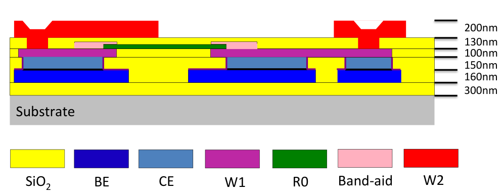
We used a three level of metal, niobium trilayer[31] process on 200 mm diameter silicon wafers to fabricate these devices. This process is an extension of the original approach used to fabricate sub-m Josephson junctions and SQUIDs using Nb-AlOx-Nb trilayers in combination with chemical mechanical polish planarization.[32] An ASML 248 nm stepper was used for the lithography of all but the pickup loop features (in W1). The pickup loop was fabricated using an ASML 193 nm scanner, which had a minimum feature size and spacing of 0.2m. A cross-sectional view illustrating this process is shown in Figure 8. All levels of metal except for the second wiring level were planarized by chemical-mechanical polishing (CMP). Briefly, the fabrication process was as follows: the silicon wafers were thermally oxidized to provide an insulating layer of 300 nm thick SiO2. A Nb/Al2O2/Nb trilayer was deposited by sputter deposition. The aluminum was thermally oxidized to provide a 1kA/cm2 critical current density for the Josephson junctions. The counter electrode of the trilayer was etched through the Al2O3 and approximately 50 nm into the Nb base electrode to form Josephson junctions and vias. A 40 nm thick layer of Nb2O5 was grown on the top surface of the trilayer, and then the base electrode was patterned by reactive ion etching. The pattern was filled with 150∘ C plasma-enhanced chemical vapor deposited (PECVD) silicon oxide and CMP’d back to the Josephson junction counter-electrode, removing the top layer of Nb2O5. The first wiring level of 100 nm of Nb was sputter deposited, patterned, filled with silicon oxide and planarized, a Au/Pd resistor layer (8 Ohms/square) was deposited and patterned by liftoff, a 100 nm thick 150oC oxide was deposited and patterned for vias, and a 200 nm thick Nb second wiring layer was sputter deposited and patterned by RIE to complete the devices. Several iterations of design, fabrication, and test were performed. In the final run, which we report on here, there was poor conductance between the first wiring and shunt levels. This required remedial “band-aid” structures of Nb to be added to make contact between the top of the first wiring level and the top of the shunt resistors. These band-aids provided extra topography, which tended to cause shorts through the intermediate insulating layer to the second wiring level, reducing our overall yield. Nevertheless, the process resulted in yields of 50% on the wafer that was most extensively tested (see Sec. IV.1). Finally a 10 m deep etch of the silicon wafers was performed, with care to keep within the thermal budget of the process. This allowed close alignment between the sample surface and the pickup loop without further processing of the SQUID sensors.
IV Device characteristics
IV.1 Electrical characteristics

Figure 9 displays typical electrical characteristics of our susceptometers, measured at 4.2 K. Fig. 9 (a) shows current-voltage characteristics for selected currents through the modulation coil. The modulation period is 0.15 mA, corresponding to a mutual inductance between the SQUID and modulation coil of 14 pH. The maximum in critical current was typically offset at random from zero flux, which we attribute to flux trapping. The maximum critical current of 45 A is close to the design value of 50 A (25A/junction). Of the 150 SQUIDs characterized on one of the 7 wafers completed, 65 were good, as judged by a measurable critical current and modulation by both field coils, representing a yield of 43%. The critical currents of the susceptometers were independent of the pickup loop radii with a maximum value of 39.7 8.5 A. The modulation depths were 0.510.01 for the 0.2, 0.6, and 2 m pickup loop SQUIDs, and about 0.35 for the 6 m SQUIDs. The average normal state resistances of the susceptometers were 1.1 0.3 . Table 1 lists the self-inductances for the SQUIDs, as a function of pickup loop inner diameter, inferred from the critical currents and modulation depths from standard SQUID theory,[33]. The inductance values for the three smallest pickup loop SQUIDs are comparable to our estimate of 50 pH from the design geometry, but the values for the 6 m pickup loop SQUIDs are surprisingly high. Two factors influence the contribution of the pickup loops to the total SQUID inductance. One is that the kinetic inductance becomes appreciable when the widths and thicknesses of the films making up the loops and leads become comparable to the penetration depth. The second factor is the length of unshielded leads. The 6 m diameter pickup loop susceptometer has about 10 m of unshielded leads, in comparison with the 2 m susceptometer, which has less than 2 microns of unshielded leads. However, this latter factor cannot explain the anomalously high inductances inferred for the 6 m susceptometers. The normal state resistances of our SQUIDs correspond to 2.2 Ohms/junction. Tesche and Clarke [21] estimate an optimized flux noise power floor from thermal sources of , which in our case suggests a flux noise of at 4.2K. Our measured white noise floors (see Figure 10) are typically about a factor of 6 higher than this estimate. The best measured flux noises are typically 2-3 times higher than the Tesche-Clark estimate, so these devices display white noise somewhat higher than anticipated.
In addition to the SQUID modulation, there are also strong step-like structures in the current-voltage characteristics of our devices that we attribute to electromagnetic resonances driven by Josephson oscillations.[34] The combination of these resonances with standard SQUID interference produces the complicated, but continuous and non-hysteretic current-voltage characteristics seen in Fig. 9. Such resonances can be reduced by incorporating a damping resistor across the coaxial leads to the pickup loops.[35]
| Pickup loop | Field coil | Shield | Analytical | Numerical | Measured | Measured | ||
|---|---|---|---|---|---|---|---|---|
| dm) | dm) | dm) | dm) | w(m) | M (/A) | M(/A) | M(/A) | L(pH) |
| 0.2 | 0.6 | 1 | 2 | 0.65 | 112.5 | 51 | 697 | 421 |
| 0.6 | 1 | 2 | 3 | 0.77 | 173 | 188 | 1664 | 43.21.6 |
| 2 | 3 | 5 | 7 | 1.22 | 555 | 728 | 59424 | 40.41.5 |
| 6 | 7 | 12 | 16 | 1.56 | 1470 | - | 159847 | 90.58 |
A good diagnostic test of our susceptometers is to measure the mutual inductances between the field coils and the pickup loops. For example, shorts between the “band-aids” and the second wiring level are difficult to detect in IV measurements, but become immediately apparent in field coil/pickup loop mutual inductance measurements. Table 1 displays various parameters for the 4 pickup loop/field coil pairs reported in this paper. Here and are the inner and outer diameters of the pickup loop and field coil, and is the width of the upper shield where the leads connect to the pickup loop. The column labeled “Analytical M” is the mutual inductance between the pickup loop and field coil calculated using the formula
| (21) |
where and are the effective diameters of the pickup loop and field coil respectively. The second term in brackets in Eq. 21 represents redirection of flux into the pickup loop from the shield. The analytical formula overestimates the redirection of flux into the pickup loop by the shield for the smallest pickup loop susceptometer. The “Numerical M” values, calculated as described in Sec. II.3.3, did not converge for the 6 m inside diameter pickup loop susceptometers because there were too few vertices in the Delauney triangulation. The “Analytical M” calculations are in reasonable agreement with experiment except for the smallest pickup loop susceptometers, while the “Numerical M” calculations are high by about 20% except for the smallest pickup loop susceptometers. The “Measured L” column represents self-inductance derived using standard SQUID theory[33] from measurements of the critical current and modulation depth.
The critical current of one of our 2m inside radius susceptometers was 44 mA. This corresponds to a critical current density of 2.75, in line with literature values[huebener1975critical], if we scale them down to our 1 m linewidth for this field coil. There was no detectable change in the noise of this susceptometer as a function of field coil current up to the critical current. Since the peak z-component of the magnetic field produced by this field coil is 0.2T/A, the largest field that can be applied by the 2m inside pickup loop radius susceptometer is about 9 mT. Our susceptometers are relatively insensitive to uniform magnetic fields: one of the 2 m inside diameter pickup loop susceptometers had an effective pickup area to a uniform field perpendicular to the device plane of 5.3 , and no detectable change in its white noise floor, albeit an increase by a factor of 2 in the noise at 20 Hz, in perpendicular fields up to 1.4 mT.
IV.2 Imaging tests

We have tested the response of our 0.2 m inside diameter pickup loop SQUID susceptometers to magnetic sources by imaging nanomagnets, superconducting vortices and lines of current, and tested our susceptibility response using a superconductor.
IV.2.1 Magnetometry
Figure 11 displays scanning magnetometry images of 3 nanomagnets with different orientations of their magnetic moment. Parameters for these nanomagnets are given in Table 2. Nanomagnet has the composition Ta(3)/Pt(5)/[Co(0.3)/Pt(1)]x5/Co(0.3)/Pt(4) (the numbers in parentheses are thicknesses in nm), and is magnetized primarily normal to the surface of the sample. Nanomagnets and are composed of CoFeB(4)/Pt(4) and are magnetized primarily in-plane. The solid lines in Fig. 11 (d)-(f) are cross-sections through the images in Fig. 11(a)-(c) as indicated by the dashed white lines.
The circles in Fig. 11 (d)-(f) represent fits to the model described in Section II.3.2, using
| (22) |
in Eq. 13 for a point dipole field source with moment , with the fitting parameters , , the number of Bohr magnetons in the nanomagnet, and the spacing between the nanoparticle and the surface of the W2 shield. The fit values for (see Table 2) are significantly below the values calculated from the measured saturation magnetization of blanket films and the known volume of the nanomagnets , indicating that the moments are not completely aligned. We did not magnetize these samples in a high magnetic field before mounting them in the SQUID microscope. These nanomagnets did, however, enable us to demonstrate the spatial resolution of our susceptometers.
The nanomagnet in Fig. 11a generates a peak flux of 0.1 through our 0.2 m inside radius susceptometer, and has a fit value for . Assuming a white noise floor of 2.7, this corresponds to a spin sensitivity of 2400 . It has become traditional to express the spin sensitivity of small SQUIDs using a simple model proposed by Ketchen,[14] in which one calculates the flux from a point dipole source through a narrow wire loop with an effective size. For example, the spin sensitivity of a square superconducting loop of side becomes[granata2016nano]
| (23) |
where is the magnetic flux noise power spectral density. This would correspond to a spin noise of 170 for our flux noise and smallest pickup loop dimensions, if we use the geometric mean diameter for the characteristic pickup loop size. The discrepancy between these two estimates indicates that care should be taken when using simple formulas for estimating spin sensitivities.
| Nanomagnet | Calc. | Fit | Fit h | ||||
|---|---|---|---|---|---|---|---|
| (nm) | (nm) | (nm) | (A/m) | m | |||
| a | 250 | 250 | 6.5 | -0.06+0.05-0.02 | |||
| b | 125 | 62 | 4 | 0.09+0.04-0.02 | |||
| c | 125 | 62 | 4 | 0.07+0.14-0.05 |
Figure 12 (a) is a magnetometry image, with a separation between SQUID and sample of about 0.1 m, of a superconducting vortex trapped in a 0.4 m thick Nb film at 4.2K. The solid line in Fig. 12 (b) is a cross-section along the dashed line in Fig. 12 (a). The circles in Fig. 12 (b) represent a fit of the model of Section II.3.2, with
| (24) |
in Eq. 13 and with a single fit parameter m - the spacing between the top of the shield layer and the surface of the sample.
Fig. 12 (c) is a cross-sectional image of a 0.8m wide current-carrying Pt thin film wire composed of a 3 segment loop, with two long segments in the -direction connected by a segment 200 m long in the -direction, imaged in contact. The solid line in Fig. 12 (d) is a cross-section along the dashed line in Fig. 12 (c). The circles in Fig. 12 (d) represent a calculation of Sec. II.3.2 for an infinitely narrow wire carrying current using the Biot-Savart law for the source field in Eq.13:
| (25) |
In this case it was assumed that the dipole and the surface were in contact. The experimental line-width in this case is slightly broader than the calculation, perhaps because of the finite width of the current carrying wire.

As mentioned above, some of the spacings derived from our fits are smaller than is physically reasonable. For example, the fit value of for nanomagnet is negative: implying that the dipole source is inside the susceptometer shield. Also, the fit heights for the vortex of Fig. 12 are smaller than one would expect, given that vortex fields should spread at the surface of a superconductor as if the monopole source is a penetration depth m below the surface of the superconductor. Nevertheless, the good agreement between the experimental and calculated cross-section line-shapes gives us confidence that we have a nearly quantitative understanding of the magnetic field response of our susceptometers.
IV.2.2 Susceptibility
Our smallest pickup loop devices have higher spatial resolution for susceptibility as well as for magnetometry. Examples are shown in Figure 13. Figure 13(a) displays susceptibility data of the pickup loop/field coil region of one of our 2 m inside radius pickup loop devices taken with our smallest pickup loop SQUID, at 4.2K, with 1 mA current through the sensor field coil, and with the sensor scanning in contact with the sample. Figure 13(b) displays the layout of the sample for comparison. The Nb film making up the pickup loop, which is 0.5 m wide, is not quite resolved in this image. Figure 13(c) shows a susceptibility image (taken under the same conditions as (a)) of a 6 m wide square Nb “pillar”. These pillars, composed of all of the layers in Fig. 8, are about 750 nm high. They are used as fill to make the chip flat on average over a scale of a few tens of microns to assist in the CMP steps. The step in susceptibility indicated by the dots in Fig. 13d has a 10% to 90% width of about 1 micron. The solid line in Fig. 13d is modeling as outlined in Sec. II.3.3, assuming a penetration depth for the pillar of 0.08 m, and with the spacing between the pillar and the surface of the susceptometer as a fitting parameter. The displayed best fit was for = 0.8 m. This value is larger than seems reasonable from other measurements and the sample-sensor geometry. In addition, the calculated cross-section is slightly broader, and with a more pronounced overshoot, than the experiment. These discrepancies may be related to the finite height of the Nb pillar. The full width of the 10% to 90% transition width was 1 m wide, significantly narrower than the 2 m full width at half maximum of the calculated field coil fields (see Fig. 7), making it appear that the spatial resolution in susceptibility is determined primarily by the pickup loop size, as opposed to the field coil size.

V Conclusions
In conclusion, we have used a tri-layer niobium, fully planarized process with 0.2 m linewidths and spacings, and a deep etch step, to fabricate scanning SQUID susceptometers with demonstrated sub-micron spatial resolution. These devices have pickup loops integrated into the body of the SQUID through well shielded, low inductance leads, integrated modulation coils for flux feedback, integrated field coils for spatially localized susceptibility measurements, and are fabricated using batch processing that produces tens of thousands of devices.
VI Acknowledgements
This work was supported by an NSF IMR-MIP Grant No. DMR-0957616. J.C.P. was supported by a Gabilan Stanford Graduate Fellowship and an NSF Graduate Research Fellowship, Grant No. DGE-114747. The nanomagnet sample fabrication at Cornell was supported by the NSF (DMR-1406333 and through the Cornell Center for Materials Research, DMR-1120296), and made use of the Cornell Nanoscale Facility which is supported by the NSF (ECCS-1542081). We would like to thank Micah J. Stoutimore for providing the Nb film used to study vortices.
References
- [1] F. P. Rogers, A device for experimental observation of flux vortices trapped in superconducting thin films, Master’s thesis, Massachusetts Institute of Technology, Cambridge, Massachusetts (1983).
- [2] L. N. Vu and D. J. Van Harlingen, Applied Superconductivity, IEEE Transactions on 3, 1918 (1993).
- [3] R. C. Black, A. Mathai, F. C. Wellstood, E. Dantsker, A. H. Miklich, D. T. Nemeth, J. J. Kingston, and J. Clarke, Applied Physics Letters 62, 2128 (1993).
- [4] J. R. Kirtley, M. B. Ketchen, K. G. Stawiasz, J. Z. Sun, W. J. Gallagher, S. H. Blanton, and S. J. Wind, Applied Physics Letters 66, 1138 (1995).
- [5] J. R. Kirtley and J. Wikswo, Ann. Rev. Mat. Sci. 29, 117 (1999).
- [6] J. R. Kirtley, Rep. Prog. Phys. 73, 126501 (2010).
- [7] C. Veauvy, K. Hasselbach, and D. Mailly, Rev. Sci. Instrum. 73, 3825 (2002).
- [8] W. Wernsdorfer, E. B. Orozco, K. Hasselbach, A. Benoit, B. Barbara, N. Demoncy, A. Loiseau, H. Pascard, and D. Mailly, Phys. Rev. Lett. 78, 1791 (1997).
- [9] A. G. P. Troeman, H. Derking, B. Borger, J. Pleikies, D. Veldhuis, and H. Hilgenkamp, Nano Letters 7, 2152 (2007).
- [10] L. Hao, J. C. Macfarlane, J. C. Gallop, D. Cox, J. Beyer, D. Drung, and T. Schurig, Appl. Phys. Lett. 92, 192507 (2008).
- [11] A. Finkler, Y. Segev, Y. Myasoedov, M. L. Rappaport, L. Ne’eman, D. Vasyukov, E. Zeldov, M. E. Huber, J. Martin, and A. Yacoby, Nano Letters 10, 1046 (2010).
- [12] D. Vasyukov, Y. Anahory, L. Embon, D. Halbertal, J. Cuppens, L. Neeman, A. Finkler, Y. Segev, Y. Myasoedov, M. L. Rappaport, et al., Nature nanotechnology 8, 639 (2013).
- [13] C. C. Tsuei, J. R. Kirtley, C. C. Chi, L. S. Yu-Jahnes, A. Gupta, T. Shaw, J. Z. Sun, and M. B. Ketchen, Phys. Rev. Lett. 73, 593 (1994).
- [14] M. B. Ketchen and J. R. Kirtley, IEEE Trans. Appl. Supercon. 5, 2133 (1995).
- [15] N. C. Koshnick, M. E. Huber, J. A. Bert, C. W. Hicks, J. Large, H. Edwards, and K. A. Moler, Appl. Phys. Lett. 93, 243101 (2008).
- [16] M. B. Ketchen, T. Kopley, and H. Ling, Appl. Phys. Lett. 44 (1984).
- [17] B. W. Gardner, J. C. Wynn, P. G. Björnsson, E. W. J. Straver, K. A. Moler, J. R. Kirtley, and M. B. Ketchen, Review of Scientific Instruments 72, 2361 (2001).
- [18] M. E. Huber, N. C. Koshnick, H. Bluhm, L. J. Archuleta, T. Azua, P. G. Björnsson, B. W. Gardner, S. T. Halloran, E. A. Lucero, and K. A. Moler, Review of Scientific Instruments 79, 053704 (2008).
- [19] M. B. Ketchen, D. D. Awschalom, W. J. Gallagher, A. W. Kleinsasser, R. L. Sandstrom, J. R. Rozen, and B. Bumble, IEEE Trans. Mag. 25, 1212 (1989).
- [20] N. C. Koshnick, J. R. Kirtley, and K. A. Moler, arXiv:1002.1529v1 .
- [21] C. D. Tesche and J. Clarke, J. Low. Temp. Phys. 29, 301 (1977).
- [22] W. H. Chang, IEEE Trans. Mag. 17, 764 (1981).
- [23] http://wrcad.com/freestuff.html.
- [24] J. M. Jaycox and M. B. Ketchen, IEEE Trans. Mag. MAG-17, 400 (1981).
- [25] “Hypres Niobium Integrated Circuit Process S45/100/200 Design Rules,” http://www.hypres.com/wp-content/uploads/2010/11/DesignRules-6.pdf.
- [26] W. C. Stewart, Applied Physics Letters 12, 277 (1968).
- [27] D. E. McCumber, Journal of Applied Physics 39, 2503 (1968).
- [28] D. J. Adelerhof, M. J. van Duuren, J. Flokstra, H. Rogalla, J. Kawai, and H. Kado, IEEE Transactions on Applied Superconductivity 5, 2160 (1995).
- [29] M. E. Huber, P. A. Neil, R. G. Benson, D. A. Burns, A. M. Corey, C. S. Flynn, Y. Kitaygorodskaya, O. Massihzadeh, J. M. Martinis, and G. C. Hilton, Applied Superconductivity, IEEE Transactions on 11, 1251 (2001).
- [30] E. H. Brandt, Phys. Rev. B 72, 024529.
- [31] M. Gurvitch, M. A. Washington, and H. A. Huggins, Applied Physics Letters 42, 472 (1983).
- [32] M. B. Ketchen, D. Pearson, A. W. Kleinsasser, C. K. Hu, M. Smyth, J. Logan, K. Stawiasz, E. Baran, M. Jaso, T. Ross, K. Petrillo, M. Manny, S. B. Brodsky, W. J. Gallagher, and M. Bhushan, Appl. Phys. Lett. 59, 2609 (1991).
- [33] A. Barone and G. Paterno, Physics and applications of the Josephson effect (Wiley, New York, 1982).
- [34] M. D. Fiske, Rev. Mod. Phys. 36, 221 (1964).
- [35] K. Enpuku, K. Yoshida, and S. Kohjiro, Journal of Applied Physics 60, 4218 (1986).