-imbalance WOM Codes for Reduced Inter-Cell Interference in Multi-Level NVMs
Abstract
In recent years, due to the spread of multi-level non-volatile memories (NVM), -ary write-once memories (WOM) codes have been extensively studied. By using WOM codes, it is possible to rewrite NVMs times before erasing the cells. The use of WOM codes enables to improve the performance of the storage device, however, it may also increase errors caused by inter-cell interference (ICI). This work presents WOM codes that restrict the imbalance between code symbols throughout the write sequence, hence decreasing ICI. We first specify the imbalance model as a bound on the difference between codeword levels. Then a -cell code construction for general and input size is proposed. An upper bound on the write count is also derived, showing the optimality of the proposed construction. In addition to direct WOM constructions, we derive closed-form optimal write regions for codes constructed with continuous lattices.
On the coding side, the proposed codes are shown to be competitive with known codes not adhering to the bounded imbalance constraint. On the memory side, we show how the codes can be deployed within flash wordlines, and quantify their BER advantage using accepted ICI models.
I Introduction
In many multi-level non-volatile memory (NVM) technologies there is an inherent asymmetry between increasing and decreasing the level to which a cell is programmed. In particular, in flash memories cell levels are represented by quantities of electrical charge, and removing charge is known to be much more difficult than adding charge. This asymmetry implies significant access limitations, whereby erasing cells must be done simultaneously in large groups of order cells (called blocks). From this limitation stem many of the serious performance issues of flash, most prominently low write rates and accelerated cell wear.
A possible solution for reducing erasure operations and increasing the lifetime of flash memories is using write-once memory (WOM) codes. The use of WOM codes in flash memories enables multiple writes before executing the costly erasure operation. Indeed, it was shown [22] that by using WOM codes in multi-level NVMs, it is possible to reduce write amplification, and thus increase the lifetime of the device. This justifies the recent extensive study of -ary WOM codes [3, 9, 11, 12, 18] that generalize the original binary WOM model [24] to multi-level flash.
In light of this promise, the main issue holding back WOM codes from deployment seems to be concerns related to inter-cell interference (ICI) [8]. Since WOM codes allow updating pages in place and non-sequentially, there is a potential risk that these updates will disturb adjacent pages. The risk of ICI disturbance becomes more significant as cell levels are updated to much higher levels than their neighbors.
Hence in this paper we propose ICI mitigating WOM codes that maintain a degree of balance between the physical levels of the cells throughout the write sequence. As a consequence, the level difference between adjacent memory cells is constrained to be up to an imbalance parameter chosen for the code.
In Section III we present our main contribution: a -imbalance -cell WOM-code construction that yields codes for general values of and input sizes. We also derive an upper bound on the number of guaranteed writes given the imbalance parameter, and show that our construction is optimal. With a comparison table we show that the numbers of writes our codes offer are favorable even relative to unconstrained existing codes. The uniqueness of this work over prior ICI codes is that it mitigates ICI within the WOM framework. Whereas known ICI-WOM codes [20] only constrain the transition of individual cells at an individual write, our codes jointly maintain balance between the symbols of the WOM codeword throughout the write sequence.
In section IV we pursue -imbalance WOM codes using the lattice-based WOM construction technique developed in [3, 4, 18]. We derive in closed form the optimal continuous write regions with the -imbalance constraint for cells and writes. The optimal boundary between the write regions turns out to be a parabola, while the known optimal boundary in the unconstrained case is known to be a hyperbola [18]. Another curious fact we find is that for the -imbalance case the optimal sum-rate is achieved by constant-rate codes, in contrast to classical unconstrained codes exhibiting a gap between optimal variable- and fixed-rate codes. The information loss from coding in short -cell blocks is minor considering the advantages. For example, it was shown [9] that when the input size of the code is order , the ratio between the -cell code’s sum-rate to the (variable-rate) WOM capacity tends to as grows.
In Section V we gear more toward practical realization of the codes and show how multiple WOM codewords can be concatenated in a flash wordline to maintain the -imbalance constraint globally. In addition, we analyze the improvement in worst-case ICI expected when cells are constrained with the -imbalance property.
II Background and Definitions
II-A Inter-cell interference (ICI)
In flash memories, changing the electrical charge of one floating-gate transistor can change the charge of its neighboring transistors through the parasitic capacitance-coupling effect [19]. This effect is referred to as inter-cell interference (ICI), and it is one of the most dominant sources for errors in flash memories. In addition, with the continuing process of scaling down cell sizes, the distance between adjacent cells becomes smaller. As a result, the parasitic capacitance between a cell and its neighbor cells increases, which in turn increases the ICI.
Moreover, as was shown in [2], the write process is also a key feature in the ICI mechanism. NAND flash devices commonly use the incremental step pulse program (ISPP) write method to mitigate cell variability [6]. In the ISPP method each program level induces a sequence of program pulses followed by a verification process to assure proximity to the target level. Each program step increases the voltage level of a cell by , which is significantly smaller than the actual voltage levels representing memory values. As was described in [2], when cells are programmed by ISPP, it is possible to compensate ICI errors in the cells that have not yet reached their target values. If during the write sequence cell causes ICI in cell , it can be detected by the verification process of cell , and the program steps of cell may be modified to compensate for this ICI. However, when a certain cell already reached its target level, ICI from a neighbor cell cannot be compensated and may cause a write error.
The accepted conclusion from the ICI behavior described above is that ICI errors are more likely when the difference between target levels of adjacent cells is high [2, 25]. Therefore, a coding scheme that balances voltage levels of adjacent cells, forbidding significant voltage differences, is likely to reduce ICI errors. Detailed analysis of the ICI and its effect on the bit-error rate (BER) appears in Section V-B.
ICI due to lateral charge spreading
Recently, a new vertical charge-trap flash memory was commercially introduced [23]. This flash device was reported to have low ICI from the capacitance-coupling effect, however, it suffers from ICI due to charge migration between adjacent cells, termed as lateral charge spreading effect. It was shown in [17] that if the level difference between adjacent cells is small, the lateral charge spreading effect is significantly reduced. Therefore, a coding scheme that balances the charge levels of adjacent cells is similarly warranted for this new form of ICI.
II-B WOM codes
Our focus in this paper is on limited-imbalance codes in the WOM model, because the in-place re-writing of WOM codes makes them especially prone to ICI. We first review some necessary background on -ary WOM codes.
Definition 1
. A fixed rate WOM code is a code applied to a size block of -ary cells, and guaranteeing writes of input size each.
A WOM code is specified through a pair of functions: the decoding and update functions.
Definition 2
. The decoding function is defined as , mapping the current levels of the cells to the data input in the most recent write. The update function is defined as , specifying the new cell levels as a function of the current cell levels and the new data value at the input. By the WOM requirement, the -th cell level output by cannot be lower than the -th cell level in the input.
Definition 3
. The code’s physical state is defined as the -ary levels to which the cells are currently programmed. The code’s logical state is the data element from returned by on the current physical state.
A write region spanned from a physical state is a set of physical states accessible from it under the WOM requirement. The size of this set we call the area of the write region. If at a given physical state the code admits more write(s), then this physical state must span a write region with area at least .
Example 1
. Let us consider two sample WOM codes. In Fig. 1 (a) we have the decoding function of constructed by Construction in [9]. This code is applied on a pair of -level memory cells, enabling guaranteed writes of size each. In Fig. 1 (b) we have a code , offering the same number of writes.
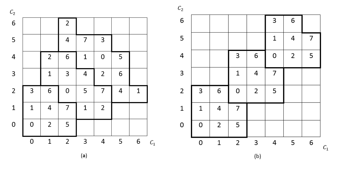
Considering Fig. 1 (a), let us assume we want to perform three writes of the logical states , and using this WOM code. For the first write the logical state is and the physical state is . When updating the logical state to , the physical state becomes . For the third write of , the physical state becomes . After the third write, we reach a physical state with level difference of between the cells. As a consequence, given that the pair of cells are adjacent, cell is likely to suffer from ICI. The code in Fig. 1 (b) maintains a better balance between the two cell levels, but will offer fewer writes if extended beyond .
In order to reduce ICI, we now define the -imbalance model for WOM codes.
Definition 4
. A -imbalance WOM code is a WOM code that guarantees that after each write the physical states of the cells , , must satisfy
| (1) |
for any write sequence.
A -imbalance code guarantees that the level imbalance between cells cannot exceed . Therefore, all cells sustain similar (same up to ) levels of charge injection, thus imposing control on the ICI disturbance. When , we get a standard unconstrained WOM code without balancing properties. As decreases, the balancing improves, but the added constraints may lead to lower re-write capabilities.
III Optimal -Imbalance Construction
Before showing our main construction, we prelude this section with a discussion on which parameters would be interesting to consider. Given and , the imbalance parameter of a code cannot be less than . That is because in any physical state, at most states are accessible for the next write while keeping the imbalance constraint. So to be able to write any of the values in the next write we must have .
Example 2
. For and , the lowest possible imbalance parameter is . It turns out that for this extreme case the simple “diagonal stacking” construction of Fig. 1 is an optimal code with writes. It is straightforward to generalize this construction to produce -imbalance codes , for any , and providing writes.
Requiring maximal balance (minimal ) results in weak codes with small numbers of writes. A better tradeoff between balancing and re-write efficiency is obtained when is relaxed from the extreme value, in which case good balancing (low ICI errors) is achieved while getting more writes. This will be the case we handle in our following construction.
III-A Construction
We now turn to present a construction where is larger than in the extreme case of Example 2.
Construction 1
. For any , we define an WOM code with , , and -imbalance parameter as follows.
- 1.
Decoding function:
The decoding function is specified in Fig. 2. The number shown at position represents the logical state as returned by the decoding function . - 2.
Update function:
The update function is specified with the aid of distinctly colored regions in Fig. 2, which represent the worst case regions of the writes. The update function determines the new physical state given the current state and the new value to be written as follows:- (a)
locate all physical states with element-wise, for which .
- (b)
is chosen as the pair that minimizes the sum of coordinates .
The bottom-left region in Fig. 2 has all logical states excluding , accessible for the first write. Each of the other two regions has all the logical states accessible from every physical state in the region to the left and down. Hence the update function supports any sequence of written values without exceeding the top-right region.
- (a)
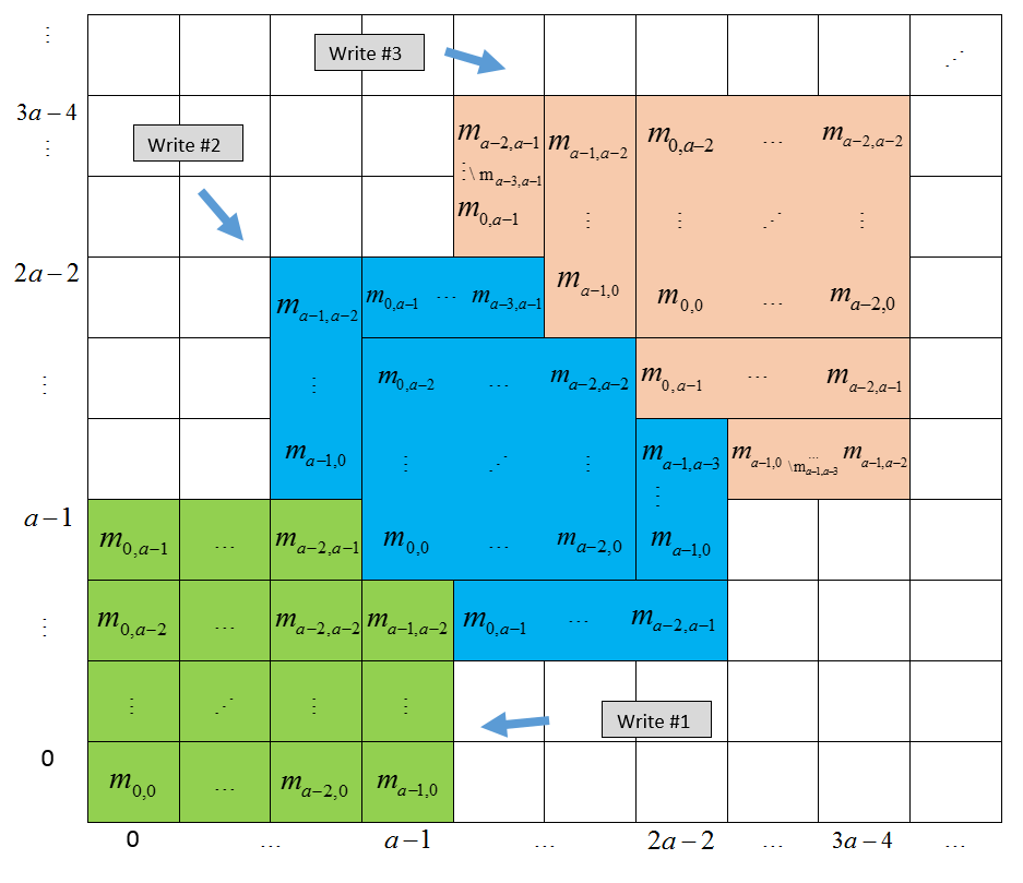
We next examine the imbalance parameter of Construction 1. It is straightforward to see from Fig. 2 that all physical states used by the update function satisfy , as required.
Before discussing the extension of Construction 1 beyond writes, we give an example for the special case .
Example 3
. In this example, we demonstrate Construction 1 for (corresponding to ), and . The writes of the resulting code are presented in Fig. 3, where the labels are given by .

It can be checked that for any sequence of written logical states the update function of Construction 1 can succeed without exceeding level at any of the cells.
Extending Construction 1 to general . To extend the decoding and update functions of Construction 1 to general , we copy the three regions of Fig. 2 and lay out the copies such that the origin of a new copy is placed on the top-right corner of the previous copy. Note that such extension requires us to relabel the logical states along the main diagonal because the origin logical state and the top-right logical state are different ( vs. ). Observe in Fig. 2 that the logical-state values on the main diagonal are of the form , and that these values do not appear elsewhere in the two-dimensional array. This means that we can lay out these values in a cyclic fashion across copies. That is, at physical state in the extended array we place logical value . Apart from the main diagonal, the extended copies of the three regions have the same assignment of logical values as the base copy of Fig. 2. In Example 3 we place the origin of a second copy at physical state , and get more writes while relabeling the main diagonal from in the first copy, to in the second copy.
We now derive the number of guaranteed writes of a -imbalance code produced by Construction 1.
Theorem 1
Proof: With the periodic extension of Fig. 2, we know that for writes, integer, is sufficient. Substituting we get as required. To complete the proof, we need to show (2) for writes, also for the cases . In these cases, the last writes each increases by . Therefore, we have
| (3) |
Substituting and rearranging, we get
| (4) |
It appears that the expression in the right-hand side of (4) may be smaller than the right-hand side of (2). We show that this cannot happen. From (3) we know that . Therefore, . Now expanding (2), we get
| (5) |
which proves (2) for all . The fact that the periodic extension of Construction 1 has is immediate from Fig. 2. ∎
III-B Upper bound on the guaranteed number of writes
We now derive an upper bound on the number of guaranteed writes of a -imbalance code that shows that Construction 1 gives optimal codes. Optimality will be proved for the special case , that is, for codes with and imbalance. A similar technique can extend the upper bound to more general values. We start with the following definitions and lemmas.
Definition 5
. If a WOM code -th write starts at state and ends at state , then the (non-negative) write sum of the -th write is defined as .
The write sum is a powerful notion because lower bounds on total write sums can give upper bounds on the number of writes. For it has been shown [9] that without balancing constraints, write sum of is both sufficient and necessary for every write. The following lemma is key to our upper bound, because it shows cases where a write sum of is necessary.
Lemma 2
. For any code , if a write starts from state satisfying , then the write region of must contain at least two states of write sum (or higher).
Proof: Let us assume w.l.o.g that the start state is state S showing on Fig. 4. All states marked as X have write sum of or less. The write sum of states A, B, and C is . Therefore, in order for the write region to have area at least , it must include at least two additional states out of A, B, C, or some other state with higher write sum.

∎
The next two lemmas show how any -imbalance code must get to the “problematic” state S of Fig. 4.
Lemma 3
. For any code , if a write starts from state satisfying , then the write region of must contain at least three states of write sum (or higher), at least one of which has or write sum at least .
Proof: Let us assume w.l.o.g that the start state is state S showing on Fig. 5. All states marked as X have write sum of or less. The write sum of states A, B, and C is . Therefore, in order for the write region to have area at least with write sum , it must include the states A, B, C, and state A has . If A is not included, then a state with write sum is required.

∎
Lemma 4
. For any code , if a write starts from state satisfying , then the write region of must contain at least two states of write sum (or higher), at least one of which has or write sum at least .
Proof: Let us assume w.l.o.g that the start state is state S showing on Fig. 6. All states marked as X have write sum of or less. The write sum of states A, B, and C is . Therefore, in order for the write region to have area at least with write sum , it must include two states out of A, B, C, and both A,C have . If neither of A,C is included, then a state with write sum is required.

∎
We are now ready to state the upper bound.
Theorem 5
. Given a -imbalance WOM code , the number of guaranteed writes is upper bounded by
| (6) |
Proof: Throughout the proof we use lower bounds on write sums, but for convenience we omit the term ”at least” when we state the value of the write sums. If write sums are strictly larger than the values quoted below, the proof is still correct, and we may even reach the desired lower bound on total write sum earlier by skipping lemmas that assume the lower quoted value. By a simple area argument, after the first write any WOM code needs to use a state with write sum . Next we show that we can invoke Lemmas 4, 3, 2 in sequence to get lower bounds on the write sums of the second, third, and forth write, respectively. Because all states with sum have at least , the conditions of Lemma 4 are satisfied after the first write (see state S in Fig. 6). By Lemma 4, after the second write any code needs a state that satisfies the conditions of Lemma 3 (see state A in Fig. 6 and state S in Fig. 5). By Lemma 3, after the third write any code needs a state that satisfies the conditions of Lemma 2 (see state A in Fig. 5 and state S in Fig. 4). Altogether we conclude that for the second, third, and fourth writes we need write sums of . From Lemma 2, after the fourth write there are two states of sum , which implies that one of them has at least , and we can again invoke Lemmas 4, 3, 2 in sequence for the subsequent three writes requiring additional write sums. Continuing this argument periodically, for writes, integer, we need a total write sum , and since , we get . Rearranging, we get as needed. To complete the proof, we need to show (6) for writes, for the cases . In this case, the last writes each requires write sum of , and we get . Because both Lemmas 4, 3 show existence of two states with write sum , one of these final states has . Thus we can tighten the relation between and to . Now we write . Rearranging, we get , and for the last inequality we used the fact that . ∎
III-C Performance comparison
Table I presents a summary of known results and bounds for -cell, WOM codes [9]. By examining the table, we can notice that for , and (which are currently the practical values of for NVMs), using Construction 1 does not compromise the number of writes compared to optimal unconstrained WOM, while it provides a better imbalance . Using constructions does compromise the number of writes for all values, including . It was also verified numerically that for , and -imbalance, codes constructed by Construction 1 reach the write-count upper bound of unconstrained codes for every value of in this range.
| q | t - Upper bound d-unconstrained | t - Construction 1 | t - Construction in [9] |
|---|---|---|---|
| 8 | 4 | 4 | 3 |
| 16 | 9 | 9 | 7 |
| 20 | 12 | 11 | 9 |
| 32 | 20 | 18 | 15 |
Actually, as we can see in the next corollary, WOM codes constructed by Construction 1 are good WOM codes even if ignoring the -imbalance property. In the following we compare Construction 1 to the best known -cell construction for general from [9].
Corollary 6
Proof: The number of writes guaranteed by Construction 1 is given by Theorem 1, while the number writes guaranteed by Construction 2 in [9] is given by
| (7) |
So, we look for the lowest value of which guarantees strictly higher number of writes for the -imbalance code. Due to the floor function applied on the number of writes, we demand that
| (8) |
This inequality holds for . Ceiling this expression ends the proof. ∎
In addition to offering strictly more writes for these values, the codes have at least as many writes as for all values of . This makes them the best known (unconstrained) WOM codes for these parameters and general (for [9] has better codes than .)
We can also notice that the number of guaranteed writes offered by Construction 1 can reach the unconstrained upper bound for some other values of and . Table II presents such pairs of , values (the values are taken in the practical range ).
| M | values of q |
|---|---|
| 15 | 9 |
| 24 | 9,10,12,13,16 |
| 35 | 11,15 |
| 48 | 13,14 |
IV Lattice-Based -imbalance WOM Codes
To present -imbalance codes in the lattice approach we start with some formal definitions.
Definition 6
. A variable-rate WOM code is a code applied to a size block of -ary cells, and guaranteeing writes, where the input size for the -th write is taken from the vector .
Definition 7
. The sum-rate of a WOM code is defined as
| (9) |
In other words, the sum rate is the total number of written bits divided by the number of memory cells.
IV-A Background and review of known results
Lattice-based WOM codes were first proposed in [18] by Kurkoski, and were further extended by Bhatia et al. in [3],[4]. In the lattice approach, the -dimensional discrete space of physical states is approximated as the continuous space . In that approximation the -th write’s input size is approximated by an area in the continuous space. Given the number of writes , the space is partitioned to disjoint regions, each allocated to a write in the sequence of writes. In the process of paritioning the space, each write is allocated an area . The objective of the partition is to maximize the product of the areas , because this would approximate maximizing the sum-rate of (9). After the continuous space is partitioned, a discretization algorithm assigns labels to discrete physical states in every region to obtain the WOM decoding function. The advantage of the lattice approach over the direct construction approach of [9] and Section III is that it can use analytic geometry to find region partitions with good properties. The key disadvantage is that optimality can only be guaranteed for the continuous approximation of the space, while the direct approach yields explicit optimal codes in the true discrete space.
In a nutshell, a -cell -write lattice-based WOM code is constructed by partitioning the -dimensional space into regions, one for each write. The first write gets allocated an area of confined between the , axes and the boundary curve (see Fig. 7). This leaves the second write an area of a rectangle confined between the boundary curve and the , lines. The boundary curve is chosen to maximize . It was shown [18] that the optimal boundary takes the shape of a rectangular hyperbola. The constructions of lattice-based WOM codes were generalized to any number of writes [4], and (non explicitly) to any number of cells [3]. In [3] the lattice approach is applied to both variable-rate and fixed-rate WOM codes. In order to make this paper cohasive, we stick with the notations of Section III (rather than those of the original papers [3],[4]) with one exception: we replace the discrete cardinalities of the input sizes with continuous cardinalities . With taking measures to avoid confusion, we slightly abuse the term sum-rate to describe the continuous areas in lieu of the discrete input sizes .
The following is a restatement of a result from [4].
Theorem 7
In the plane the optimal boundary of Theorem 7 is given in closed form as the curve . This optimal boundary was derived as follows. Let us assume the optimal boundary between the two writes is given by some function . is the area under while is calculated as the area of a rectangle formed by some point on with the and lines (see Fig. 7).

In order to get the optimal sum-rate code, we need to find the boundary that brings to a maximum. Given that each point on can span a rectangle with different area, is the minimum of the areas of all possible rectangles. Therefore, the following optimization problem [4] is solved
| (12) |
where is the maximal value of the support of . The solution of (12) gives the hyperbola boundary of Theorem 7.
After deriving the continuous boundaries between the writes, the WOM code is constructed by discretization and a label assignment algorithm.
Example 4
. Let us consider the following WOM code [3] . This code is applied on a pair of -level memory cells, enabling guaranteed writes of input sizes and for the first and second writes, respectively. The decoding function of this code is presented in Fig. 8.
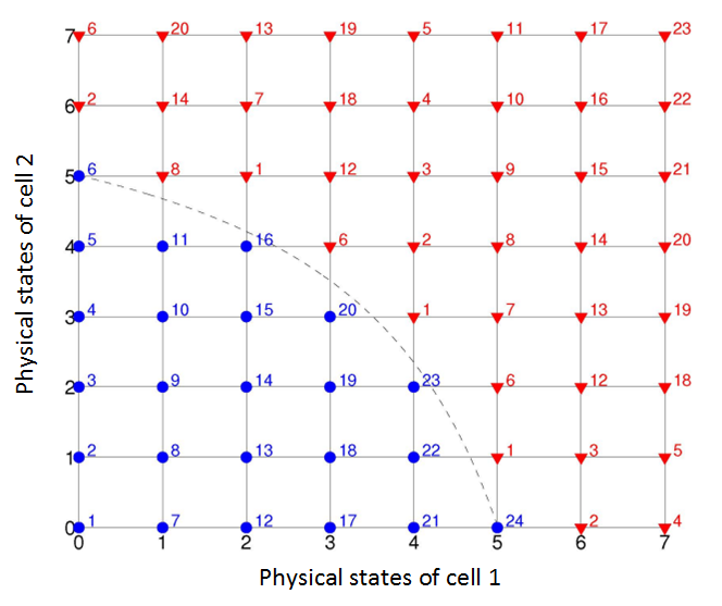
The boundary between the two writes is the following hyperbola:
| (13) |
IV-B Construction for lattice-based -imbalance WOM codes
In this sub-section we present a construction of -imbalance WOM codes after applying the imbalance model (Definition 4) to the continuous approximation of the lattice approach. Our main result toward that is a closed-form characterization of the optimal boundary for -cell -write -imbalance WOM codes.
Theorem 8
. When , the optimal boundary for a maximal sum-rate -imbalance lattice-based WOM code is given by , satisfying
| (14) | |||
and the optimal sum-rate is given by
| (15) |
It can be checked that (14) implies that the curve is a parabola.
Before proving this Theorem we present the following lemmas. The first lemma finds the shape of the boundary that yields for the second write identical areas among the points on the boundary. Note that with the -imbalance constraint the areas are bounded by the lines , in addition to the bounding by the lines and in the unconstrained case (see Fig. 9.)
Lemma 9
. Given a -imbalance lattice-based WOM code with , the boundary that yields identical values for all points on is given by
| (16) | |||
Proof: The constraint induced by the -imbalance model is that all the valid physical states are bound by the lines , as can be seen in Fig. 9. Therefore, is a function on which every point spans an equal-area shape with the , and lines. We now turn into calculating this area. First we have the area of a rectangle (denoted by dashed lines in Fig. 9) given by .

From this rectangle we need to subtract the area of the two triangles. It is easy to verify that the area of the top triangle is given by and the area of the bottom triangle is given by . Subtracting these areas and equating to the cardinality of the second write yields (16). Note that for the two subtracted triangles to exist, the coordinate of the intersection point between and must be at most . Given that the intersection point is , we get that in order for the triangles to exist we need
| (17) |
After some manipulations we get that the condition (17) is equivalent to given in the Lemma statement. ∎
The second lemma finds the relation between the areas of the first and second writes for boundaries in the form given in Lemma 9.
Lemma 10
. For a given in (16), the cardinality of the first write is given by
| (18) |
Proof: The cardinality of the first write is the area bound by the and axes, the lines, and from (16). Due to the symmetry of the problem, we first calculate the area between and the line . Then we subtract the area between and , and finally we multiply the outcome by . In order to do so, we first calculate the intersection points between and the lines and . It is easy to verify that the intersection points are and , respectively. Therefore, the desired area can be calculated by
| (19) | |||
¿From Lemma 9 it is not hard to see that for , is given by
| (20) |
Substituting this in (19) gives the expression
| (21) | |||
∎
With the help of Lemmas 9 and 10, we can now prove Theorem 8.
Proof:
In order to find the maximal sum-rate of with imbalance parameter , we now need to adjust the optimization problem of (12) to the -imbalance model, and to find the values of and that maximize . By a similar argument to the one proved in [4], the minimization in (12) implies that the optimal sum-rate boundary must satisfy the identical-area condition of Lemma 9. Then among the curves of Lemma 9 parametrized by , the corresponding value of is determined by Lemma 10. This implies that
| (22) |
Taking the derivative of the right-hand side with respect to and equating to gives
| (23) |
There are two interesting conclusions from Theorem 8. First is that the introduction of the -imbalance constraint changed the shape of the curve from a hyperbola to another regular shape: a parabola. Second is that for the -imbalance case the cardinalities that maximize the sum-rate turn out to be the fixed-rate cardinalities. This favorable property does not exist in the unconstrained case (for unconstrained WOM the fixed-rate property costs sub-optimality in sum-rate). We next show an example of a code constructed with the help of Theorem 8 followed by the discretization step.
Example 5
. Let us consider the following -level -cell -write -imbalance WOM code with imbalance parameter of , . By Theorem 8, the optimal boundary is given by
| (24) |
The continuous cardinalities corresponding to the boundary of (24) are . But after discretization we obtain in Fig. 10 discrete cardinalities (it is possible to have because a point can be in the region without its entire unit square). In particular, the resulting WOM code is not fixed-rate even though the continuous boundary is fixed-area. The decoding function of is presented in Fig. 10.
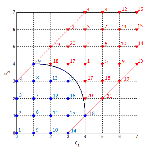
The sum-rate of the non-balanced code of Example 4 (with the same , and ) is . By constraining the code with the imbalance parameter the sum-rate in Example 5 is reduced to ( reduction). Let us now compare the lattice-based results to direct -imbalance WOM codes constructed by Construction 1. To obtain a code from Construction 1 with , the largest rate parameter is , corresponding to . This gives a code , which has a sum-rate of , lower than the lattice-based construction for this example.
IV-C Performance Comparison
We now compare the unconstrained lattice-based WOM codes of [3],[4] with the new lattice-based -imbalance WOM codes. We make the comparison over the continuous sum-rate calculated from , (before discretization). Table III presents the sum-rate of the codes for different values of and . The reader can notice that when the imbalance takes the highest value allowed by Theorem 8: , the sum-rate is compromised by approximately . Naturally, when decreases the sum-rate decreases due to the more limiting constraint imposed by the -imbalance model.
=1mm q 8 - 3.97 8 3 3.75 8 2 3.42 16 - 6.17 16 6 5.91 16 5 5.76 16 4 5.54 16 3 5.29
V Wordline ICI Reduction by -imbalance WOM Codes
To this point, we have presented code constructions that bound the imbalance between two memory cells. In flash practice, many more than two cells are updated together in a memory page, also called a wordline. To match the write granularity of the flash architecture, we will use a code on each pair of adjacent cells in a wordline. Hence, a wordline includes concatenated pairs of WOM-coded cells, as depicted in Fig. 11.

In the sequel we say that a set of cell levels is -balanced if they satisfy the -imbalance constraint of (1).
V-A Inter-codeword balancing
As can be seen in the following example, simple concatenation of codewords (of two memory cells each) does not guarantee that the -imbalance property is maintained between any pair of adjacent cells.
Example 6
. Let us assume we code two adjacent pairs of cells in the same wordline by the -imbalance WOM code presented in Fig. 3. Suppose the first pair holds the logical state of by the physical state , and the second pair holds the logical state of by the physical state . To this end, all four cells are -balanced. Now, suppose that in the next wordline update we wish to only update the logical value of the second pair from to . Therefore, the physical state of the first pair remains at while the physical state of the first pair is updated to . Therefore, the four cell levels are no longer -balanced because the two center cell levels are apart.
In order to keep the -imbalance property among all the cells in the wordline, it is possible to use WOM codes with the synchronous property [5], which means that each of the writes has a disjoint set of physical states. This way, it is guaranteed that none of the codewords remain in the same physical state through the write sequence, and balance is maintained across codewords as well. However, requiring the synchronous property compromises the sum-rate relative to non-synchronous WOM codes with the same code parameters.
Interestingly, as we show next, we can maintain the -imbalance property while using the (non-synchronous) Construction 1 with a more clever wordline update process. We start with some formal definitions and a proposition.
Definition 8
. Given a code applied to a wordline with cells, is defined as the wordline data vector of the -th write, where the elements of are the logical states of the codewords. We also define as the physical states vector of the -th write, where the elements of are the physical states of the codewords.
Definition 9
. A physical state is called a frontier state of the -th write if it can be reached after writes, and no other state with , can be reached after writes.
Informally, frontier states are the “worst” states to be in after writes, and the only ones we need to consider for the code correctness.
Definition 10
. The frontier states of the -th write are denoted by the set . The subset of frontier states that can be accessed from the physical state is denoted by .
Example 7
. Let us consider the -imbalance WOM code whose decoding function is given in Fig. 3. The frontier states of the first write are . The frontiers of the second and third writes are given by and , respectively.
Our objective now is to present an update process that guarantees that after each write all the cells in the wordline are -balanced. In particular, every pair of adjacent cells – both within and across codewords – will be -balanced. The following proposition provides the basis for that update process.
Proposition 11
. Let us consider a -imbalance WOM code constructed by Construction 1. If is a frontier state of the -th write, and is a frontier state of the -th write, then all of satisfy the -imbalance constraint.
Proof: Due to the periodic nature of , it is sufficient to prove the statement for the first three writes only. From Fig. 2 we can see that the frontiers of the first write are . The frontiers of the second and third writes are given by and , respectively. It can now be easily verified that any pair of levels taken from are at most apart. ∎
The implication of Proposition 11 is that it is sufficient to keep all the physical states in a wordline between frontier states of two adjacent writes and , inclusive of states of both frontiers. This is achieved by the wordline update process given in Algorithm 1.
In simple words, Algorithm 1 guarantees that after writes every physical state in the wordline will be at least in a frontier state of the -th write (and at most in a frontier state of the -th write). We now prove the correctness of the wordline update process.
Theorem 12
Proof: We prove that after writes every physical state is bounded (element-wise) from above by an frontier state and from below by an frontier state. This claim together with Proposition 11 would establish the theorem statement. By Algorithm 1, the update function is invoked with a physical-state argument from . So trivially by the WOM property the output of the update function must be bounded from below by a state in . By the properties of the code, for any the output of is bounded from below by a state in . ∎
Example 8
. Let us now return to Example 6. The example begins with two logical states and stored in two adjacent codewords of . After updating the second logical state from to , the physical states were no longer -balanced. However, if we use Algorithm 1 for update, the physical state of the first (not updated) logical state becomes , which is the nearest physical state representing starting from a frontier state of the first write. The physical states are now , and they satisfy the -imbalance constraint.
V-B ICI analysis
We now analyze the ICI reduction by using a -imbalance WOM code. We start with some background concerning the noise model and bit-error rate calculations.
V-B1 Noise model
As was previously explained, different memory levels are represented by different levels of electrical charge or voltage. Due to many inherent physical limitations [7],[21], these voltage values include noise. As a consequence, each memory level is distributed over a range of voltages around the desired voltage level. The most common and simple model for flash voltage distributions is the Gaussian model, whereby a cell voltage level is one of discrete levels plus an additive Gaussian noise .
During read operation, the memory level is determined by a sequence of comparisons of the cell voltage level to some reference voltage levels [13]. Therefore, the bit-error rate (BER) is given by [14]
| (25) |
where is some normalized reference level between two adjacent voltage levels, and the function is
| (26) |
V-B2 ICI model
A recent work [8] combined a theoretic ICI model with empirical measurements and presented a practical model for ICI. According to this model, the threshold voltage change of some victim cell is given by
| (27) |
where and are fitting coefficients, and is the threshold voltage of the victim cell before interference. It was shown in [8], that practically the coefficients are significant for up to three closest neighboring cells only. Therefore, a cell is likely to suffer ICI if there is a significant voltage change in one of its closest neighboring cells.
However, as was described in section II, the ISPP (incremental step pulse program) write process is also a key feature in the ICI mechanism. In the ISPP method each program level induces a sequence of program pulses followed by a verification process to assure proximity to the target level. Each program step increases the voltage level of a cell by , which is significantly smaller than the actual voltage levels representing memory values. The voltage raise due to a single program step can be modeled [26] by adding a uniform random variable in the range of . The program process that includes a sequence of program steps is thereby modeled by the sum of such uniform random variables, giving the well-known Gaussian shaped voltage level distributions, when .
Proposition 13
. The ICI noise of a victim cell, due to program steps in a nearby aggressor cell, is an Irwin-Hall distributed random variable, with mean and variance , where is the capacitance ratio between the two cells and is the ISPP voltage step.
Proof: The ICI noise is the sum of independent random variables uniformly distributed over multiplied by the capacitance coupling [26].
| (28) |
The sum of uniformly distributed independent random variables is Irwin-Hall distributed random variable [16]. Its mean is the sum of the means and its variance is the sum of the variances. ∎
As was described in [2], when cells are programmed by ISPP, it is possible to compensate ICI errors in the cells that have not reached their target values. If during the write sequence the aggressor cell causes ICI in the victim cell, it can be detected by the verification process of the victim cell leading to canceling excess program steps. However, when a certain cell reached its target level, updating its neighbor cell can still cause ICI.
Proposition 14
. Let us consider two adjacent -ary cells with additive Gaussian voltage noise read by the normalized threshold voltage . Let us now assume that in some ISPP operation, the target voltage levels of the two cells are and where . The BER of the victim cell, due to ICI, at the end of the write operation is given by
| (29) |
where , and is the capacitance coupling between the two cells.
Proof: As was described, ICI effects can be compensated during ISPP operation as long as both cells have not reached their target voltage levels. Therefore, the number of program steps with a potential ICI effect is . Assuming , the ICI noise approaches the Gaussian distribution, and substituting this in Proposition 13 gives the mean and variance of the distribution and , respectively. As a result, given an additive Gaussian noise , the total noise is the sum of two independent Gaussian random variables distributed as
| (30) |
To simplify in (30), we recall that the distribution noise is itself a result of the ISPP pulses raising the voltage level from to , taking steps. This gives by an argument similar to Proposition 13. In addition, we can take , hence
| (31) |
Given that , we can approximate . Applying the BER calculation of (25) gives (29). ∎
The main conclusion from this ICI model is that ICI errors are more likely when the difference between voltage levels of adjacent cells is high. Therefore, (29) motivates the -imbalance WOM codes we study here.
V-B3 BER improvement
We now analyze the ICI reduction by using a -imbalance WOM code. We analyze the worst-case ICI scenario, in which cells with guaranteed -imbalance are compared with the extreme ICI case: a victim cell in erased state with neighboring aggressor programmed to level .
Theorem 15
. Using a -imbalance WOM code on a wordline of -ary memory cells reduces worst-case ICI BER by multiplicative factor
| (32) |
where is the variance of the voltage distribution, is the normalized reference level for read, is the voltage shift of the victim cell for a worst-case scenario unconstrained write, and , are negative constants.
Proof: The maximal voltage shift of the victim cell of an unconstrained write corresponding to updating level to level is given by . By using the -imbalance WOM codes, the maximal voltage shift is given by . Therefore, by using (29) we get
| (33) |
Let us now use the following approximation [1] for the function valid for
| (34) |
where and are given by and respectively. By using this approximation and simplifying, (33) becomes,
| (35) |
By examining Theorem 15, we can first notice that the negative term in the exponent is negligible due to which is relatively small. Therefore, we can see that the the ICI BER improvement due to using -imbalance codes increases exponentially when the imbalance parameter decreases.
Example 9
. The BER values for this example are taken from [25], where we assume that these values are also valid for . Initial raw BER of yields . After P/E cycles, the BER becomes due to ICI. That means the normalized voltage shift due to ICI is . Using a the -imbalance WOM code reduces the worst-case normalized voltage shift to . Therefore, the new improved BER is given by
| (36) | |||
That means, the BER due to ICI was improved by factor relative to the unconstrained write.
VI Discussion and Conclusion
VI-A Bitline ICI
We have shown how -imbalance codes hold a potnetial to significantly reduce ICI within a wordline. This is likely sufficient for the ICI seen in 3D vertical charge-trap flash memories (described in the Introduction). However, standard floating-gate flash memories also suffer from significant bitline ICI. Therefore, in order to reduce ICI in floating-gate flash memories, the -imbalance WOM codewords must also be balanced with WOM codewords in adjacent wordlines. We leave this interesting problem as future work.
VI-B Application to wear leveling
The same -imbalance properties suggested here for ICI reduction turn out to be useful for another important problem of flash storage: wear leveling. Due to limited lifetime of flash cells, it is essential to avoid exceeding the recommended write counts. In order to avoid a scenario in which some pages are worn faster than others, a wear-leveling technique is incorporated to the page mapping layer. This provides good inter-page wear leveling [15]. However, within a page cells can differ significantly in their wear (the total amount of charges written to them so far). These differences may be detrimental to the data reliability, as read/write procedures are commonly tuned to the wear state of the page. Using a WOM code with the -imbalance property can help equalize the intra-page wear, because no cell will be programmed to a level much higher than the rest of the page.
VI-C Conclusion
In this work we presented -imbalance WOM codes designed to reduce inter-cell interference in multi-level NVMs. Constructions that are simple to implement were given and analyzed. We also derived an upper bound on the number of guaranteed writes of a -imbalance WOM code and showed that our proposed construction is optimal for some parameters of the code. Lattice-based constructions were also derived and characterized in closed form for writes. Future work can include extending the presented two-cell WOM codes to WOM codes for , and the lattice-based codes also to .
VII Acknowledgment
This work was supported by the Israel Science Foundation, by the Israel Ministry of Science and Technology, and by a GIF Young Investigator grant.
References
- [1] M. Benitez, and F. Casadevall, “Versatile, accurate, and analytically tractable approximation for the Gaussian Q-function, ” IEEE Trans. on Communications, vol.59, no.4, pp. 917-922, April 2011.
- [2] A. Berman and Y. Birk, “Constrained Flash memory programming, ” in Proc. of IEEE Int. Symp. on Information Theory (ISIT), pp. 2128-2132, July 31 - Aug. 5 2011.
- [3] A. Bhatia, M. Qin , A.R. Iyengar, B.M. Kurkoski, P.H. Siegel, “Lattice-based WOM codes for multilevel flash memories,” IEEE J. Sel. Areas Commun., vol.32, no.5, pp. 933-945, May 2014.
- [4] A. Bhatia, and P.H. Siegel, “Multilevel 2-cell t-write Codes,” in Proc. of IEEE Inform. Theory Workshop (ITW), pp. 247-251, Lausanne, Switzerland, Sep. 2012.
- [5] N. Bitouze, A. Graell i Amat and E. Rosnes, “Using short synchronous WOM codes to make WOM codes decodable,” IEEE Trans. on Communications, vol.62, no.7, pp. 2156-2169, July 2014.
- [6] J. Brewer and M. Gill, Nonvolatile Memory Technologies with Emphasis on Flash. IEEE Press Series on Microelectronic Systems, 2001.
- [7] Y. Cai, et al. “Error patterns in MLC NAND flash memory: Measurement, characterization, and analysis,” in Proc. of IEEE Design, Automation & Test in Europe Conference & Exhibition (DATE), pp. 521-526, March 2012.
- [8] Y. Cai, O. Mutlu, E.F. Haratsch, and K. Mai, “Program interference in MLC NAND flash memory: Characterization, modeling, and mitigation, ” in IEEE 31st Inter. Conf. on Computer Design, pp. 123-130, Oct. 2013.
- [9] Y. Cassuto, E. Yaakobi, “Short q-ary fixed-rate WOM codes for guaranteed rewrites and with hot/cold write differentiation,” IEEE Trans. Inform. Theory, vol.60, no.7, pp. 3942-3958, July 2014.
- [10] R. L. Corless, G. H. Gonnet, D. E. G. Hare, D. J. Jeffrey, and D. Knuth, “On the Lambert W function,” Adv. in Comp. Math. 5(4):329–359, 1996.
- [11] R. Gabrys, E. Yaakobi, L. Dolecek, S. Kayser, P.H. Siegel, A. Vardy, and J.K. Wolf, “Non-binary WOM-codes for multilevel flash memories,” Proc. IEEE Inform. Theory Workshop, pp. 40-44, Brazil, Oct. 2011.
- [12] K. Haymaker and C.A. Kelley, “Geometric WOM codes and coding strategies for multilevel flash memories,” arXiv:1206.5762v1, May 2012.
- [13] E. Hemo and Y. Cassuto, “Adaptive threshold read algorithms in multilevel non-volatile memories,” IEEE Journal on Selected Areas in Communications, vol.32, no.5, pp. 847-856, May 2014.
- [14] K. A. S. Immink and J. H. Weber, “Detection in the presence of additive noise and unknown offset,” in Proc. of IEEE Inter. Conference on Communications (ICC), pp. 431-435, 8-12 June 2015.
- [15] A. Jiang, R. Mateescu, E. Yaakobi, J. Bruck, P.H. Siegel, A. Vardy, and J.K. Wolf, “Storage coding for wear leveling in flash memories,” IEEE Trans. Inform. Theory, vol. 56, no. 10, pp. 5290–5299, Oct. 2010.
- [16] N.L. Johnson, S. Kotz, and N. Balakrishnan, Continuous univariate distributions, vol.2, Wiley, New York, 1995.
- [17] Y. Kim, et al. “Modulation coding for flash memories, ” in Computing, Networking and Communications (ICNC), 2013 International Conference on, pp. 961-967, 28-31 Jan. 2013.
- [18] B. Kurkoski, “Lattice-based WOM codebooks that allow two writes,” in International Symp. on Inform. Theory and its Applications, Honolulu, Hawaii, pp. 101-105, Oct. 2012.
- [19] J.D. Lee, S.H. Hur, and J.D. Choi, “Effects of floating-gate interference on NAND flash memory cell operation,” IEEE Electron. Device Lett., vol. 23, no. 5, pp. 264–266, May 2002.
- [20] Q. Li, “WOM codes against inter-cell interference in NAND memories,” in Communication, Control, and Computing (Allerton), 49th Annual Allerton Conference on, pp. 1416-1423, 28-30 Sept. 2011.
- [21] N. Mielke, et al. “Bit error rate in NAND flash memories,” in Proc. of IEEE Int. Reliability Physics Symp. (IRPS), pp. 9-19, April 27 - May 1, 2008.
- [22] S. Odeh and Y. Cassuto, “NAND flash architectures reducing write amplification through multi-write codes,” IEEE 30th Symposium on Mass Storage Systems and Technologies (MSST),pp. 1-10, June 2014.
- [23] K.T. Park, et al. “A world’s first product of three-dimensional vertical NAND Flash memory and beyond, ” in 14th Annual Non-Volatile Memory Technology Symposium (NVMTS), pp. 1-5, 27-29 Oct. 2014.
- [24] R. L. Rivest and A. Shamir, “How to reuse a write-once memory,” Information and Control, vol. 55, no. 1, pp. 1-19, Dec. 1982.
- [25] V. Taranalli, H. Uchikawa, and P.H. Siegel, “Error analysis and inter-cell interference mitigation in multi-level cell flash memories,” in Proc. of IEEE Inter. Conference on Communications (ICC), pp. 271-276, 8-12 June 2015.
- [26] Q. Xu, et al. “Modelling and characterization of NAND flash memory channels,” in Measurement, vol.70, pp. 225-231, 2015.