An Integrated Circuit for Radio Astronomy Correlators
Supporting Large Arrays of Antennas
Abstract
Radio telescopes that employ arrays of many antennas are in operation, and ever larger ones are being designed and proposed. Signals from the antennas are combined by cross-correlation. While the cost of most components of the telescope is proportional to the number of antennas , the cost and power consumption of cross-correlation are proportional to and dominate at sufficiently large . Here we report the design of an integrated circuit (IC) that performs digital cross-correlations for arbitrarily many antennas in a power-efficient way. It uses an intrinsically low-power architecture in which the movement of data between devices is minimized. In a large system, each IC performs correlations for all pairs of antennas but for a portion of the telescope’s bandwidth (the so-called “FX” structure). In our design, the correlations are performed in an array of 4096 complex multiply-accumulate (CMAC) units. This is sufficient to perform all correlations in parallel for 64 signals (=32 antennas with 2 opposite-polarization signals per antenna). When is larger, the input data are buffered in an on-chip memory and the CMACs are re-used as many times as needed to compute all correlations. The design has been synthesized and simulated so as to obtain accurate estimates of the IC’s size and power consumption. It is intended for fabrication in a 32 nm silicon-on-insulator process, where it will require less than 12 mm2 of silicon area and achieve an energy efficiency of 1.76 to 3.3 pJ per CMAC operation, depending on the number of antennas. Operation has been analyzed in detail up to . The system-level energy efficiency, including board-level I/O, power supplies, and controls, is expected to be 5 to 7 pJ per CMAC operation. Existing correlators for the JVLA () and ALMA () telescopes achieve about 5000 pJ and 1000 pJ respectively using application-specific ICs in older technologies. To our knowledge, the largest- existing correlator is LEDA at ; it uses GPUs built in 28 nm technology and achieves about 1000 pJ. Correlators being designed for the SKA telescopes ( and ) using FPGAs in 16 nm technology are predicted to achieve about 100 pJ.
keywords
radio astronomy, correlators, arrays, integrated circuit, ASIC†Corresponding author.
; ; ; Published 2016 March 18.
1 Introduction
As radio telescopes get larger, there is a need to provide digital signal processing electronics that are smaller and less power-hungry than would be implied by the extrapolation of existing designs. This is especially true of correlation, which grows as for antennas and processed bandwidth . The ALMA telescope in Chile Wooten & Thompson (2009), with and GHz, currently has the largest correlator by this measure, but much larger ones are planned. Table 1 gives some properties of the correlators of existing and planned telescopes, including . This paper presents the design of an application-specific integrated circuit (ASIC or IC or chip) that enables construction of power-efficient correlators at large . The design provides considerable flexibility in that the IC can be used to construct correlators for a wide range of telescope sizes, from to essentially unlimited.
[h] Some Radio Telescope Correlators, Existing and Future \topruleTelescope Status Technology Year* ** , MHz , W , Hz , pJ Notes \colruleVLA obsolete ASIC 1975 1.5 27 200 50,000 2.92E+11 171,000 a JVLA existing ASIC 130 nm 2005 4 32 8,000 70,000 1.64E+13 4,270 b ALMA existing ASIC 250 nm 2002 3 64 8,000 65,000 6.55E+13 992 c LEDA existing GPU 28 nm 2011 4 256 57.55 7,370 7.47E+12 977 d CHIME existing GPU 28 nm 2013 4 128 400 10,080 1.31E+13 769 e SKA1-low proposed FPGA 16 nm 2017 8 512 300 11,600 1.57E+14 74 f SKA1-low ASIC 32 nm 2015 4 512 300 752 1.57E+14 4.8 g SKA1-mid proposed FPGA 16 nm 2017 4 197 5,000 40,000 3.88E+14 103 h SKA1-mid ASIC 32 nm 2015 4 197 5,000 4,928 3.88E+14 12.7 k SKA2*** planned (TBD) 2021 TBD 2000 5,000 TBD 4.00E+16 (TBD) m \botrule
- •
All power estimates are for correlation only, at system level, including power supply loss but not including cooling.
- •
* Design freeze year.
- •
** Input number quantization, real or imaginary part. See section 2.1.
- •
*** Parameters are not yet well defined, so the values here are speculative.
- a
https://public.nrao.edu/gallery/radio-telescopes/image?id=300.
- b
McKinnen (2010) and other sources; see also Perley et al. (2009).
- c
130 kW system Baudry & Webber (2011), approximately half for correlation.
- d
- e
Denman et al. (2015). Water cooled. Data are for the CHIME Pathfinder; the full CHIME telescope will be larger.
- f
Bunton (2015). Preliminary power estimate, probably within a factor of two of the final value.
- g
This work. Not equivalent to the currently proposed implementation due to smaller . Correlator ICs: 1.95 W = 284 W. Support chips, power, control (est.): 468 W.
- h
Carlson (2015). Preliminary power estimate, probably within a factor of two of the final value.
- k
This work. Power is for . Correlator ICs: W = 1292 W. Support chips, power, control (est.): 3636 W.
- m
https://www.skatelescope.org/projecttimeline/.
Figure 1 is a simplified depiction of the signal processing required for a generic multi-antenna telescope.

There are usually input signals because each antenna collects radiation in two orthogonal polarizations. Each signal is converted to baseband and digitized, forming a time series of complex numbers at rate . The processing is separated into operations performed on each signal separately and operations used to combine the signals. Here we consider correlation as the combining method11 1 Other combining methods, such as beamforming, are sometimes used, but correlation is often preferable because it allows forming an image by Fourier synthesis Thompson et al. (2001). Under special circumstances, combining via a spatial Fourier transform may be advantageous Tegmark (2009) Morales (2011).. The rate of operations on individual signals is proportional to , so correlation dominates at sufficiently large . This paper concerns only correlation.
A correlator performs a complex multiply-accumulate (CMAC) operation on each sample of each pair of signals. The total rate of CMAC operations is then (including correlation of each signal with itself22 2 The self-correlations produce real results and require only half the resources of a CMAC, so each physical multiply-accumulator can be configured to perform one cross-correlation or two self-correlations per cycle. We exploit this in our design, and operations are counted accordingly.). A good figure-of-merit (FoM) for power efficiency is then , where is the total power consumed. Table 1 shows this FoM for each telescope (where only the power of the correlator proper, as shown in Fig. 1, has been included). At the IC level (including all on-chip overhead and I/O), our design achieves 1.78 pJ at . Table 1 includes estimates of the system-level FoM (including board-level I/O, power supplies, etc.) that would be achieved if correlators for the proposed SKA telescopes were based on this IC. The design is most efficient when is a multiple of 64, so it is particularly inefficient for SKA1-mid at . Nevertheless, it would provide a substantial improvement over FPGA-based designs.
Figure 2 is a simplified block diagram of an individual CMAC unit.

It consists of a multiplier, an adder, and an accumulation register. The product of each pair of samples is added into the accumulator for a fixed number of sample clocks , then the accumulator content is copied to the output and the accumulator is cleared to begin another accumulation cycle or “integration.” Although each CMAC is straightforward, there are various architectures for organizing many CMACs to produce a large correlator. The total CMAC rate is the same for all architectures, but the rates of other necessary operations (including memory writing and reading for temporary buffering of data and chip-level I/O) depend on the architecture. A detailed study D’Addario (2011) has shown that the chip-level architecture of Figure 3

leads to the lowest system-level power consumption. It achieves this by minimizing the rates of the auxiliary operations. The architecture includes CMACs arranged as an array and a memory that holds a block of input samples from all signals. When the total number of complex correlations to be computed () is larger than the number of CMACs (), the CMACs are re-used as many times as necessary by re-reading data from the buffer. We call each computation of correlations one “sub-integration” (SI), and SIs are needed to compute all the correlations of one full integration, where is called the CMAC re-use factor.
In practice this architecture requires that the buffer memory and CMAC array be on the same chip because of the high data rate between them. The memory reading rate is times higher than its writing rate, and this can easily lead to an impractical transfer rate if the CMAC array were on a separate chip. (In our design, the transfer rate is up 352 Gb/s.) Even if the transfer rate is practical, several orders of magnitude more energy is required to move a bit between chips than within a chip.
Modern telescopes are too large for all correlations to be done in one IC, so the architecture must provide a way to partition the processing among many of them. If each device has CMACs running at clock rate , then devices are needed. One way to partition them is to have each device handle a subset of the signals, but then a copy of every signal sample must be delivered to at least devices, leading to high total I/O rate and increased power consumption. The favored architecture avoids this by having each device process all signals (even if is large) but only a subset of the samples of each signal. The samples could be decimated in time, but this would require another step in which the partial accumulations for the same signal pair are added across devices. Instead, the samples are decimated in frequency. Each signal is first processed by a uniform filter bank to separate it into at least independent channels of bandwidth (Fig. 3). Each device then processes part of the bandwidth. Because of the CMAC re-use, each device can handle input sample bandwidth . The filter bank could provide more than channels (but preferably an integer multiple of ), in which case each device can process several channels sequentially so that it still processes bandwidth . For further discussion of the reasons that this architecture is preferred and for descriptions of alternatives, see D’Addario (2011).
In this paper we describe a particular IC implementation that follows this architecture and takes additional steps to minimize power consumption. Most existing synthesis telescopes whose correlators were considered large at the time of their design have used ASICs (including the original VLA, the expanded JVLA, the VLBA, and ALMA), but in those cases the ASIC was tailored to the particular requirements of one telescope. Our design strives to be useful for a wide variety of future telescopes by supporting almost any number of antennas and any total bandwidth.
The design targets a 32 nm CMOS silicon-on-insulator process from IBM, 32SOI IBM (2009), where it will have a silicon area less than 12 mm2. The logic is specified in code written in Verilog, so in principle it could be ported to other processes, but our use of certain hard macros from IBM is not portable. In particular, a high-density dynamic RAM is a critical component of the design.


Figure 4 summarizes the IC’s performance over a wide range of . These results are discussed in more detail in section 5. Results are computed for and each multiple of 64 up to 4096. Except for , which is a special case, the best performance occurs at , where the device is utilizing its maximum input and output data bandwidths, but good performance is maintained over the full range. In particular, the energy FoM achieves very nearly its minimum value of 1.76 pJ at many values of out to arbitrarily large values. There are some unfavorable values of where the device cannot be used as efficiently, such as when is a prime number, but even then the performance remains good. For an ideal device (where the processing rate remains constant and there is negligible overhead), the bandwidth decreases as . Fig. 4 shows that the upper envelope of bandwidth vs. approaches this limit.
The remainder of this paper consists of an overview of the design (Section 2), design details (3), synthesis and simulation results (4), performance as a function of (5), system integration (6), and conclusions (7).
2 Design Overview
2.1 Selection of fixed parameters
To create a specific design within the chosen architecture, it is necessary to select the number of CMACs , the memory size, and the maximum input and output rates. In general, more of everything is better, but there are practical limits to chip size and chip power dissipation, and compromises are needed to control cost. If the IC were being designed for a fixed number of antennas , more optimization would possible. For example, Figure 5 shows a model of power consumption per unit bandwidth vs. memory size and number of CMACs when .
Although power decreases monotonically for increasing and , the improvement is slow beyond Mb (at 8b per signal sample) and . For larger , it is better to have more memory, even at the cost of fewer CMACs. However, it was the objective of our design to support a wide range of . That is, we wanted the IC to be usable in multiple future telescopes whose sizes are not known in advance. We chose and Mib, largely because this leads to a chip size that can be fabricated in an available process at an acceptable cost and yield. It is shown in section 5 that the resulting design is useful from to .
It is also necessary to choose the digital representations of the input and output data. Each is a complex number, and we represent them as two twos-complement numbers with half of the bits used for the real and imaginary parts. We choose b for the input sample (4 b real and 4 b imaginary) and b for the output result (16 b and 16 b).
For the inputs, large words are expensive since the size and power consumption of the CMAC multipliers increases as . Conversely, large words provide smaller quantization noise and larger dynamic range. With 4 b numbers, quantization adds 1.2% to the noise in measurements of cross-power between Gaussian-distributed random processes at the optimum signal levels (Thompson et al., 2001, Table 8.2, page 276), and most correlator designs have recognized the diminishing returns of finer quantization33 3 Even 1 b (2 level) quantization is possible, and is used in some spectrometers Van Vleck & Middleton (1966). VLBI has traditonally used 1 b and 2 b (4-level) quantization. The original VLA correlator used 3 levels or “1.5 bits” D’Addario et al. (1984), the ALMA correlator uses 3 b, and the JVLA and LEDA correlators use 4 b. See also Table 1. Signal levels can be maintained near optimum by level controls in the filter banks or other up-stream circuitry. Dynamic range is usually not a consideration in radio astronomy, since the signals are Gaussian-distributed processes with known variance. An exception is when a signal includes unexpected interference. Nearly all interference is human-generated, and those signals almost always have narrow bandwidth (%) compared with astronomical observations (% to near 50% in modern telescopes). This can be exploited in FX processing (Fig. 3) where each signal is partitioned by frequency; those channels that are contaminated with interference can be ignored. This may require maintaining high dynamic range (wide data words) in the per-signal processing, including the filter banks, but not in the correlator.
For the output words, size must be sufficient to avoid overflow during accumulation. In our design, the internal accumulators are 20 b+20 b and 21 b wide for cross- and self-correlations, respectively. The maximum number of accumulations per integration is such that this is sufficient, even if the signal variances are more than 9 dB above optimum. The accumulators are rounded to 16 b before delivery to the outputs. Analysis shows that the rounding error is far smaller than the uncertainty caused by the intrinsic noisiness of the signals D’Addario (2015a). (See additional discussion in section 3.2.)
2.2 Block diagram
Figure 6 is a high-level block diagram of the IC.

Assume that the memory and CMAC array operate on the same clock. On each clock cycle, one sample from each of row signals and column signals is read from the memory and presented to the CMAC array, which computes all cross-products and adds them to their respective accumulators. After cycles, the accumulators are read out, completing one sub-integration. Data are re-read from the memory for subsequent SIs until all correlations of the signals have been computed, completing one integration. Meanwhile, new data for the next full integration are being written to the memory from the input. Because data in the memory are being re-used over SIs, the memory’s write rate is slower than its read rate. The data output rate depends on the integration length , which is limited by the size of the memory.
Figure 7 is a more detailed block diagram, showing individual modules of the implementation and all input/output signals.

Input data are received at DATAIN, which is a 32 b bus synchronized to the rising edge of CLKIN. On each clock, four 8 b samples of different signals at the same sampling time are received. INTEGRATE, also synchronized to CLKIN, marks the start of a new integration. The input module collects 32 of these 32 b input words in a buffer, producing a 1024 b word that is delivered to the memory module for writing to the RAM. Successive input words supply samples from other signals and other sampling times in a particular order until all samples of one integration have been received and written to the memory. The address generator module determines the sequencing of write and read cycles and provides the appropriate addresses for each. It also provides synchronization signals that organize the chip’s computations into sub-integrations. The address generator is logically the most complex part of the design, although it uses very little silicon area; it is further described in the next section. On memory read cycles, the RAM delivers 1024 b words to a small buffer which organizes the data into -bit words corresponding to the rows and columns of the CMAC array (for details see section 3.4). The CMAC array module performs the correlations as previously described. At the end of an SI, 4096 complex results are available. These are delivered sequentially by the output module to 16 parallel output pins synchronous with 8192 cycles of CLKOUT. SYNCOUT is asserted during the first CLKOUT cycle of each SI.
Most of the modules are driven by an internal clock called sysclk, synthesized in the clock generator module from CLKIN using a phase-locked loop (PLL). Each cycle of sysclk is either a memory read cycle, memory write cycle, or an idle cycle, as determined by the address generator module. The frequency of sysclk must be sufficient to keep up with the input data. During read cycles only, the CMAC array computes the appropriate correlations; otherwise it is idle. The clock generator can also generate outclk for use by the output module and as output signal CLKOUT. Alternatively, the output clock can be supplied externally at input USROUTCLK, in which case that signal is passed through clock generator to outclk.
The control module contains a set of twelve 20 b registers that can be written and read by the user over a 4-wire serial peripheral interface (SPI) bus Motorola (2003). These registers contain data for programming the PLL to set the frequencies of sysclk and outclk, as well as data needed by the address generator to determine the address sequence, including the values of and .
2.3 Operation
The ability to control the clock frequencies and the address generation parameters provides considerable flexibility, making the chip useful for a wide range of . The integration length is also determined by a user-controlled register. The frequency-decimation (FX) architecture of Fig. 3 allows building a correlator of almost any total bandwidth.
Re-use of the CMACs follows a particular pattern, illustrated in Figure 8 for the case of (256 signals).

In this figure, each square represents the same CMACs performing one SI. The SIs form a half-matrix with the signals delivered to each row and column in groups of . There are groups. For the SIs along the diagonal, only half of the CMACs are needed to correlate the signals of a group with each other. Therefore, the other half of the CMACs is used simultaneously for the correlation of another group. During these SIs, the CMAC array operates in “split mode,” which is further described in section 3.2. In this way, only SIs are needed, not .
It is desirable for to be an integer, and we will see later that it is best if is even. To use the chip with a number of signals that produces non-integer , it is necessary to supply dummy signals so that the total number is a multiple of . Although the chip’s throughput is only as large as it would be if the dummy signals contained valid values, its power consumption can be smaller. If the dummy signals are always set to zero, no switching activity occurs within the CMAC array when they are being processed so no dynamic power is used. We will show (sections 4.5 and 5) that the majority of the power is used by the CMAC array.
The SIs can be computed in any order without changing the total computation effort, but the design uses a particular order so as to make efficient use of the memory. This is illustrated in Figure 9, again for the case of , .

Each of the four groups of signals is placed in a block of contiguous memory addresses, occupying words of 1024 bits. The SIs are computed column-wise, beginning with the diagonal SI at the upper left of the diagram and proceeding downward. The illustration shows computation of the third SI, involving signal groups 1-64 and 129-192. Note that signal group 1-64 is needed for all four SIs of the first column, but when that column is complete that group is never needed again. Therefore, as soon as the first column is complete the section of memory used for that group can be overwritten with data for the next full integration. Similarly, when the second column is complete, the second memory block can be overwritten with new data. Furthermore, data from the third and fourth groups is not needed for the current integration until SIs 3 and 4, so it can be written during SIs 1-4, as illustrated in Figure 10(a), which plots the memory addresses for reading column data, for reading row data, and for writing new data as a function of clock cycle number over two complete integrations.
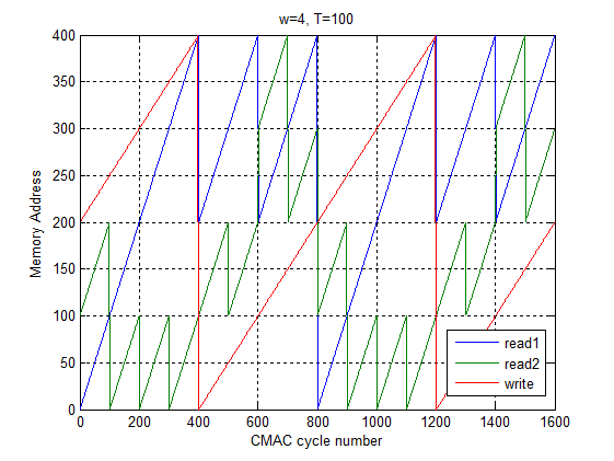
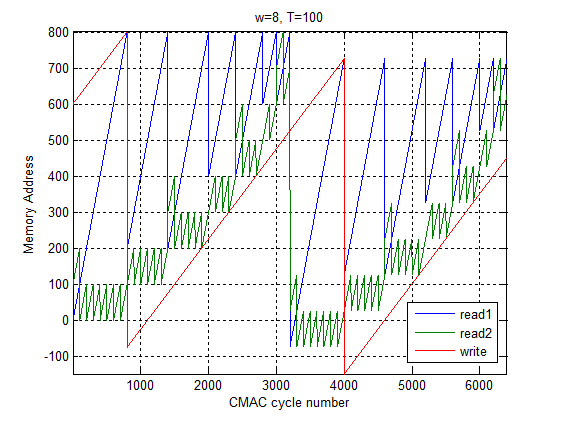
We see that complete overlap of reading and writing is achieved, with no need for double-buffering in order to have continuous operation. Unfortunately this result cannot be extrapolated beyond ; to process more signals continuously, some additional memory is needed to buffer new data so that it does not overwrite data that are not yet fully processed. For example, Figure 10(b) shows the situation for , where 9.4% additional memory is needed. The additional memory requirement increases with but never exceeds 33%, so full double-buffering (100%) is not necessary. The overlapping of reading and writing also means that the latency in delivering the results of an integration is less than the integration length; for example, at [Fig. 10(b)] an integration is complete and all results are delivered to the ouptut 57 SIs (rather than 64 SIs) after the last data for that integration are delivered to the input. In general, the latency is SIs.
This arrangement allows each block of memory to use a sequential set of addresses. To compute one SI, we need only know the starting addresses of the row data (for reading), the column data (for reading), and the new data (for writing), each of which is simply incremented throughout the SI. The starting addresses are given in control registers and are incremented automatically in the address generator logic and delivered to the memory in the proper sequence. The user is required to update the three addresses via the SPI bus prior to the start of the next SI. This is easily done with SPI clock rates that never exceed 15 MHz, although the chip is designed to support SPI rates of at least 25 MHz.
2.4 Performance
Performance is often limited by input or output bandwidth, as shown in Section 5. Results given in this paper are based on achieving input and output clock frequencies of 500 MHz, or 16 Gb/s over 32 input pins and 8 Gb/s over 16 output pins. SPICE simulations D’Addario (2015c) show that this is easily achievable to or from a typical modern FPGA Altera (2015) via a wire-bond or flip-chip package and a 76-mm-long printed circuit board trace. Considerably higher rates may be achievable if differential signaling is used for CLKIN and CLKOUT. At I/O speeds of 500 Mb/s per pin, the best performance is achieved at , where the bandwidth per chip is 1.5625 MHz and the total chip power is 2.26 W, giving a energy figure-of-merit of 1.76 pJ per CMAC operation.
3 Design Details
3.1 Dynamic memory
The selection of dynamic RAM (DRAM) for the on-chip memory was an important design choice. The desired 64 Mib could lead to a large and expensive chip unless a high-density memory is used. The DRAM available for the IBM 32SOI process achieves 2.8 times higher density than static RAM (SRAM) in the same process. Even so, it occupies 65.5% of the cell area in our design. We considered other processes at about the same technology node and found that the available SRAMs had similar or lower density. Few offered DRAM. Therefore, use of SRAM was found to be unfeasible for the selected memory size. Power was also a consideration; the selected DRAM uses only 14.3% to 19.4% of the chip’s power, depending on . Use of a smaller memory was also considered, but it was found that this would require proportionally lower CMAC clock speed and bandwidth in order to maintain feasible output data rate. Indeed, performance could be improved at large with more memory, so the selected size is already a compromise.
We restricted ourselves to processes for which multi-project wafer runs are available. It is important to fabricate and test prototype devices before proceeding to production, and it is our judgment that funding for a dedicated prototype run would not be obtainable nor would it be justified.
Use of DRAM implies several design difficulties, including constraints on the sequence of read and write addresses and the need for periodic refreshing. The DRAM has a concurrent refresh feature that allows refreshing to be overlapped with reading and writing, so in principle it is possible to avoid any refresh-only cycles. However, the retention time is finite and this leads to a minimum clock speed of 200 MHz. In addition, the DRAM version that we chose has a constraint that the same bank may not be addressed on successive clock cycles. Each bank carries 2048 addresses, so our 65,536-address memory contains 32 banks. On each clock cycle, it is necessary to supply the read or write address along with the refresh bank address (CRA in Fig. 7); this is done by the address generator. Every bank must get 256 refresh cycles within the retention time. We have devised an algorithm that meets all constraints and guarantees refreshing all banks provided that the clock rate is at least 227 MHz. If the total of the read rate and the write rate is at least this high, then no refresh-only cycles are needed. Otherwise, is set to 227 MHz and the excess cycles are refresh-only. During refresh-only cycles, the memory uses much less dynamic energy than during read or write cycles, and the CMACs use no dynamic energy because they are not clocked.
3.2 Complex multiply-accumulator array
Our implementation of an individual CMAC is shown in Figure 11.

The inputs and are each 4b+4b complex numbers ( in Fig. 11) in twos-complement form, with new values delivered at each clock. To avoid any d.c. offset in the input data while retaining twos-complement representations, we assume that the range of the real and imaginary parts is [--7,+7]; that is, --8 is excluded. The complex multiplier is implemented with four real multipliers and two real adders44 4 Complex multiplication can also be implemented with three real multipliers and five real adders Mahdy (1999). This can be advantageous when multiplication requires substantially more logic than addition, as happens with larger numbers but not with the 4 b numbers used here. Besides, the four-multiplier version facilitates implementation of the CMAC split mode, discussed later in this section., producing complex products that are no more than 8b+8b in twos complement (). Each product is added into a 20b+20b accumulator () for clock cycles. On the next clock after that, signal sync is asserted; this causes the real and imaginary accumulator contents to be rounded to 16 bits each () and loaded into a holding register until they can be delivered to the output, and at the same time the product of the next pair of input samples is loaded directly to the accumulator, thus starting a new accumulation.
The accumulator size is chosen to avoid overflow in cross-correlation of Gaussian-distributed signals. When correlating such signals, there is an optimum signal strength that minimizes quantization noise in the results; for 4 b numbers, that optimum is a standard deviation of on both the real and imaginary parts (Thompson et al., 2001, Table 8.2, page 276). It has been shown D’Addario (2015a) that even when the standard deviations of both signals are (9.5 dB above optimum) overflow does not occur at 20 b until , even when the correlation coefficient is unity at the worst-case correlation phase.55 5 In these calculations, overflow refers to the expected value of the accumulation, so the results are statistical. Whereas the number of accumulation cycles is many thousand, the actual value is, with high probability, within a few percent of the expected value. At , overflow does not occur provided that the correlation coefficient is less than 0.27, also at and worst-case phase. For our design, the memory size ensures that for . High cross-correlation coefficients are rarely seen in radio astronomy (where is routine), but in situations where they can occur the signal level can be reduced upstream of the correlator. If overflow does occur, the design ensures that it is detected. A check for overflow is done on every clock, and if it ever occurs the final result is set to the maximum positive or negative value, as appropriate.
The rounding logic reduces the results from 20b+20b to 16b+16b by rounding off the 4 least-significant bits. The mid-point is always rounded away from zero so that no bias is introduced66 6 The cross-correlations have random phase, so the real and imaginary parts are symmetrically distributed about zero. For the self-correlations, which are always positive, unbiased rounding is not possible with deterministic logic. In practice, that bias is negligible because self-correlation values are large.. Rounding is acceptable to the extent that it does not cause loss of significance when the correlation coefficient is small. Analysis shows D’Addario (2015a) that the quantization error due to rounding will be smaller than the intrinsic noise in the result provided that when the signal strengths are 9.5 dB below optimum, even if the true correlation coefficient is zero. For our design, we are limited to at all , otherwise the output data rate would exceed the available output bandwidth. This means that the rounding never introduces significant quantization noise.
When the CMAC array is computing sub-integrations on the diagonal of the SI half-matrix (Fig. 8), it must operate differently. The array then contains three versions of the CMAC cell: CMACs below the diagonal are computing cross-correlations among the signals of one group (the “row” signals); those above the diagonal are computing cross-correlations of another group (“column” signals); and those on the diagonal are computing two self-correlations at once, for one signal from each group. The latter is possible because self-correlations accumulate the squared magnitude of the signal, and this can be done using only half the resources of a CMAC (two of the four real multipliers in the complex multiplier, and only the real part of the complex accumulator). The other half of this CMAC is then used simultaneously to compute the self-correlation of a signal form the other group, accumulating its real result in the “imaginary” part of the accumulator. This amounts to a re-organizing of the CMAC array when a diagonal SI is being computed. We call this the “split mode” of the CMAC array, and it is controlled by a signal from the address generator called “CMAC mode” in Fig. 7.
Self-correlation is equivalent to cross-correlation with a correlation coefficient of unity, so overflow can occur more easily. On the other hand, the result is always positive so the accumulator can be considered unsigned; this allows to be twice as large before overflow occurs. Nevertheless, to allow without overflow when the signal strength is 9.5 dB above optimum requires 21 b. Therefore, our implementation provides 21b+21b accumulators for the 64 CMACs on the diagonal, since they are the only ones that do self-correlations (and 20b+20b accumulators for the other 4032 CMACs). In split mode only, those CMACs round off 5 least-significant bits rather than 4 so that the result is still bits.
3.3 Clocks
To compute all the correlations of one integration, a total of CMAC operations is required, and since of them are done at once, this requires a total of CMAC clocks. At the same time, input data samples for the next integration must be received and written to the memory. Each memory word carries samples, so memory write cycles are needed. It follows that a memory write cycle is needed for every CMAC cycles. Since we also need one memory read cycle for each CMAC cycle, we need memory cycles (read+write) for each CMAC cycles. Since 32b samples are received on each input clock, input clocks are needed for each memory write. From this we find that
where is the input clock (INCLK) rate and is the memory clock (sysclk) rate. If sysclk is faster than this minimum, the address generator automatically causes the extra cycles to be refresh-only cycles for the memory and idle cycles for the CMACs.
The CMAC clock is a gated version of sysclk so that it is active only during memory read cycles. Otherwise all CMACs are idle and consume no dynamic power.
After each SI, 8192 cycles of the output clock are needed to read out the 16b+16b complex results from the 4096 CMACs over the 16 b DATAOUT bus. This must be done before the next SI is complete, which means that
where is the outclk rate.
Both sysclk and outclk can be synthesized internally from INCLK using a PLL in the clock generator, but this is subject to some constraints. There is only one PLL; it contains an internal delay-controlled oscillator in the range 3–6 GHz locked to , where and are integers determined by user-settable registers. The oscillator drives two separately-programmable frequency dividers, one of which generates sysclk. Then outclk is either generated by the other divider or supplied by the user at input pin USROUTCLK. The two divider ratios and the selection of the outclk source are configurable via the SPI interface.
3.4 Address sequence
The memory word size of 1024 b or 128 samples was selected so that there is one memory read cycle for each CMAC cycle. However, one CMAC cycle requires 64 row samples and 64 column samples, so it would have been more straightforward to have 512 b (64 sample) memory words and perform two reads per CMAC cycle, one for the row data and one for the column data, which are always at different locations in memory (Fig. 9). Then the maximum CMAC rate would be limited to half the maximum memory rate, which would limit performance because the CMACs can operate much faster. To avoid this limitation, we use wider memory words, but then some data reordering is needed between the memory and the CMAC array. That is the purpose of the buffer module (Fig. 7).
Each memory word contains simultaneous time samples from different signals along with the next time samples from the same 64 signals. Each subsequent word contains two more time samples, so that words contain all samples for those signals. Similar blocks of words hold samples for other groups of signals, with groups altogether (Fig. 9). Reading from memory to buffer is done in sets of 4 successive clock cycles, obtaining time samples through for the row signals and the column signals: {unnumlist}
Memory to Buffer
row data containing samples for and
row data for and
column data for and
column data for and . On the next 4 clock cycles, the same data are transferred from the buffer to the CMAC array for processing, but in a different order: {unnumlist}
Buffer to CMAC Array
row and column
row and column
row and column
row and column . The buffer size is 8 memory words (double buffering) so that memory reading and CMAC processing can be overlapped with a latency of 4 clock cycles.
Processing uses sets of 4 words rather than 2 in order to ensure that no memory bank is addressed on two successive cycles.77 7 This constraint arises because of internal pipelining in the memory. A version of the DRAM without pipelining could have been used, avoiding the constraint, but it would then have been considerably slower, limiting chip performance under some circumstances. Performance of the current design is always limited by I/O bandwidth, not by the speed of the DRAM or CMACs. The 16 b memory address is structured as
address[15:0] = {withinBank[10:0], bankNumber[4:0]}.
By always reading two adjacent addresses on successive cycles, we are assured that those cycles access different banks.
As explained earlier, a write cycle for new data must occur for every read cycles. The shortest possible complete sequence then includes sets of four read cycles ( cycles) and two write cycles, as illustrated in Figure 12.
The two write cycles use adjacent addresses, so the bank access constraint continues to be satisfied. The sequence then includes cycles, and such sequences are needed to complete a sub-integration.
This structure introduces two constraints on user parameters. First, must be even so that the sequence can include sets of read cycles. This means that must be a multiple of . Second, must be a multiple of because each sequence contains time samples.
The constraint that must be a multiple of 64 is mitigated for small numbers of antennas by a special “memory bypass mode” that supports (64 signals) by bypassing the memory entirely and sending input data directly to the CMAC array. Two sets of 64 signals are processed in parallel, e.g. from different frequency channels. Bypass mode is selected by a bit in a user-controlled register. Thus, the chip can efficiently support , 64, 128, 192, . For other values of , dummy signals (preferably always zero) must be added88 8 It would be possible to avoid the requirement that be even and thus allow to be any multiple of 32 by lengthening the processing sequence. If memory writing were done in sets of 4 addresses rather than 2, then each sequence would include read sets and could be any integer. This would exacerbate the constraint on , which would then need to be a multiple of ..
On each cycle, the memory is given not only an address for reading or writing, but also a concurrent refresh bank number. The latter must be different from the bank in the current, previous, and next read or write address, as well as different from the current, previous, and next refresh bank. It is tricky to meet this requirement while ensuring that all banks get refreshed sufficiently often. Our algorithm for this is not necessarily optimum, but it is reasonably efficient in that it requires a clock rate only about 13% higher than an ideal one that distributes all cycles uniformly among the banks.
3.5 Synchronization
Once the appropriate memory addresses are written to the control registers, the chip processes each sub-integration automatically, delivering the results at the OUTDATA pins over 8192 cycles of CLKOUT. Output signal OUTSYNC is asserted when the first word of each SI is valid. The frequency of OUTCLK must be high enough to deliver all 8192 words before the next SI is completed. OUTCLK can be faster, in which case more than 8192 cycles will occur before the next assertion of OUTSYNC, but only the first 8192 output words are valid. The internal processing runs on sysclk, whose frequency must be fast enough to keep up with the input data. It can be faster, in which case idle cycles are automatically inserted by the address generator module. In this way, the overall speed of operation is determined entirely by INCLK.
The chip does not automatically keep track of full integrations; it operates at the SI level. To establish the integration-level sequence (Figs. 9, 10), the user must supply the starting memory addresses of the row data, column data, and input (write) data for each SI, along with a bit that specifies whether this SI uses split mode. This is done by writing to particular registers over the SPI link. Values written during the current SI are used during the next one. Writing may be begin immediately after OUTSYNC is asserted, and must be completed before the current SI is finished, as indicated by the next assertion of OUTSYNC.
Updating the addresses for each SI could have been further automated within the chip rather than putting that burden on the user, but the chosen design ensures that the chip has great flexibility. It allows a wide range of to be supported, and it allows a different memory address sequence than that shown in Fig. 10 to be used if desired. A somewhat different sequence, discussed in section 5.1, is useful when is sufficiently large; this permits the chip to support arbitrarily large .
Internal synchronization signals are needed to account for the processing latency of each block in the signal flow. These are shown as blue lines in Fig. 7. The input module requires 32 CLKIN cycles to collect enough data to write one 1024-b word to the memory. At the beginning of an integration, it delivers a delayed version of INTEGRATE to the address generator module when the first word is ready to be written to the memory. The address generator then provides a signal marking the start of the first SI as well as subsequent SIs. This signal is passed through the memory module, where it is delayed by the memory’s read latency (but not otherwise used), and similarly through the buffer module, and then to the CMAC array, where it forces each CMAC to copy its accumulator to its readout register and to ready the accumulator for the next SI (Fig. 11). The synchronization signal is then passed to the output module, where it is delayed by the output latency and delivered to the SYNCOUT pin at the same time as the first output word of the SI is delivered to DATAOUT.
3.6 Inputs and Outputs
The selection of parallel, synchronous bit streams for the main data input and output is a compromise driven by cost. Simulations D’Addario (2015c) in SPICE Nagel & Pederson (1973) have shown that at least 500 Mb/s can be transferred between each pin and a modern FPGA via a wire-bond package and 76 mm-long printed circuit trace. Somewhat higher rates may actually be achieved, but 500 Mb/s has been used for the performance calculations of this paper. The number of pins is limited by package cost and size as well as timing skew. We selected 32 input pins and 16 output pins, providing 16 Gb/s input bandwidth and 8 Gb/s output bandwidth. These bandwidths provide good performance for all , as shown in section 5 and Fig. 4. To achieve higher rates would require multi-Gb/s serial transmitters and receivers. Such devices are technically feasible, but including them in the present design is cost prohibitive. (An ab initio design would be difficult and risky for our small team, and existing designs command high license fees.) Larger input bandwidth would permit a higher processing rate at small , and larger output bandwidth would do so at large . This would reduce the chip count in a large system, but it would have little effect on the system power consumption.
The design includes 39 input pins and 19 output pins (Fig. 7), not including power, ground, and test connections. All are implemented with the same bi-directional I/O cell from IBM. It provides a low-voltage CMOS interface at a nominal voltage swing of 0.9 V, which is the same as the nominal supply voltage of the internal logic. Each cell is configured internally as either input or output, since none of our pins is bi-directional. For outputs, it is configured for maximum slew rate and 50 ohm source resistance. Additional discussion of these cells is given in Section 4.4.1.
3.7 Control Interface
The chip is controlled by a set of 12 registers that can be written or read over a 4-wire SPI slave interface Motorola (2003). It is intended to be driven by a corresponding SPI master interface in an external controller, such as an FPGA. Multiple correlator chips on the same board can be connected to the same controller; one of the wires (SSEL) selects the current correlator chip.
Each register contains 20 bits. Our protocol uses 25 SPI clock cycles per transfer (4 address bits, one write enable bit, and 20 data bits). On each transfer, all bits of the addressed register are read and returned over the SPI MISO (master in, slave out) wire. Data sent on the MOSI (master out, slave in) wire are then written to the register if the write enable bit is set. A portion of one register has a set of read-only status bits for reporting error conditions. Once set by the internal logic, the status bits remain set until that register is read, then they are automatically cleared. Register reading and writing are driven entirely by the SPI clock (wire SCLK), generated by the master interface, independent of any other clocks. This ensures that they can be set even if the internal PLL is not running or is unstable because it was previously misprogrammed or because INCLK is not yet being supplied.
At power-up or after assertion of active-low RESETN, the registers are loaded with default values which allow operation to proceed. Unless the defaults happen to correspond to the present application, the output data will not be valid until the registers are written with the appropriate values. These include programming the PLL to generate sysclk at a frequency high enough to keep up with the input data, and specifying the values of and , which determine the addressing sequence (Fig. 12) and the SI length. In most applications, these settings need only be written during initialization.
Three registers must be written during each sub-integration. These give the starting addresses for column data reading, row data reading, and new data writing during the next SI, and whether the next SI uses split mode. This requires 75 cycles of SCLK, and must be completed during the time of one SI, which is CMAC clocks, so there is a minimum value of that varies inversely with the SPI clock rate and the CMAC rate. The maximum CMAC rate is 312.5 MHz at (see Section 5). At an SCLK clock rate of 15 MHz, this gives . The memory size is sufficient to support at . The CMAC rate and maximum are such that an SCLK rate MHz is sufficient at all , and the chip will support an SCLK rate of at least 25 MHz.
4 Synthesis and Simulation
4.1 Methodology
The register-transfer-level (RTL) design was created in Verilog. Three vendor-specific hard-macro cells were instantiated:
- –
DRAM, , a black-box macro from IBM. Two of these are used in parallel inside the memory module to create a memory.
- –
PLL, also a black-box macro from IBM, used in the clock generator module.
- –
Bi-directional LVCMOS input/output cell, from IBM.
The design was synthesized using standard cell libraries from ARM99 9 ARM Ltd., product SMC9MC, HVt, SVt, and UVt versions ARM (2015). by means of Synopsys Design Compiler1010 10 DC Ultra, Version K-2015.6 Synopsys (2015)., with timing constraints based on MHz, MHz, and MHz. Except for its use of the above cells from IBM, the RTL design is portable and could be synthesized for fabrication in a different process by using an appropriate standard-cell library.
Library files giving timing and power data on all standard cells and on the above special cells were available for various process-voltage-temperature corners. During synthesis, we used a “slow” corner at drain-source voltage 0.8 V (cf. 0.9 V nominal) and temperature --40 C. The resulting synthesized netlist and the calculated delays of all cells and nets were then used by ModelSim1111 11 ModelSim SE-64 version 10.6c for Linux Mentor Graphics (2015). to simulate operation of the chip for a specific scenario ( antennas and integration length ) and a specific set of simulated input signals. The simulation test bench collected the chip’s output data and these were later compared against independently-calculated correct results. The simulator also calculated the switching activity on each net. The switching activity was read back into Design Compiler and its Power Compiler component was used to calculate the power dissipated by each cell. For the latter calculation, we used a more practical corner (0.9 V and +50 C) in order to obtain realistic switching and leakage power estimates.
Three versions of the standard cell libraries were available, each containing cells of the same functionality but at different CMOS threshold voltages. The compiler was told that cells from the highest-threshold library are preferred, since this minimizes leakage power, but it was allowed to select up to 10% of the cells from the lower-threshold libraries when optimizing timing. The final result used 6.17% from the low-threshold libraries.
Design Compiler was used in its Topographic Mode, where it makes use of data about the process technology (metal layer stackup) and physical data about all the cells (dimensions and port locations) to perform a rough placement of the cells. This allows it to make accurate estimates of the delay and capacitive load of each wiring net. Although a complete layout has not yet been done, we believe that this provides reliable power estimates.
The results of this process are summarized in Table 4.1. {wstable}[h] Preliminary Power and Cell Area, and \toprule Module Power, mW Area, mm2 Switching Internal Static Total \colruleCMAC Array 129.199 179.727 36.500 345.386 2.728296 Memory 2.970 123.994 10.000 136.983 6.392190 Input cells (39) 3.702 0.331 0.286 3.257 0.200353 Output cells (19) 33.391 6.248 0.139 39.774 0.131266 Clock Generator 0.875 0.013 54.000 54.880 0.078929 Control 0.000 0.005 0.006 0.012 0.001333 Output 12.943 3.766 5.490 22.196 0.102880 Buffer (DRAM to CMACs) 2.024 7.860 0.572 10.457 0.034140 Address Generator 0.021 0.116 0.016 0.153 0.000704 Input 2.051 6.650 0.286 8.988 0.012865 Misc. (top module) 3.981 0.000 0.695 4.530 0.07335 \colruleTotal of all modules 191.156 327.619 107.989 626.617 9.756312 \botrule
- •
Clock buffer trees not included, see Section 4.3
- •
As expected, a majority of the power is used by the CMAC array (55%) and the memory (22%). Static power, mostly due to cell leakage currents, is low. Nearly all of the power of the clock generator is static, but in that case it is not leakage but rather is due to the PLL’s internal microwave oscillator, which runs even without input switching activity. More than 65% of the cell area is occupied by the memory; the design would be impractical if lower-density memory (e.g., static RAM) were used.
We have found that several small corrections to these results are necessary. First, the clock networks were treated as ideal during synthesis, so buffer trees for them were not synthesized. Therefore, we carried out a rough, manual synthesis of the clock trees for the purpose of estimating their power consumption and area. Second, the simulator did not provide enough switching activity detail to determine accurately the internal power of the memory. This had only a small effect in the simulated scenario, but it is significant when the results are extrapolated to other scenarios, as we do in section 5. Third, the I/O cell power estimates from Power Compiler are inaccurate for several reasons, so we re-computed those manually. This produced only a small net change. Details of these corrections are described sections 4.3 and 4.4 and the final results are given in section 4.5.
4.2 Post-Synthesis Simulation
The compiler generated a synthesized netlist and a Standard Delay Format IEEE (2001) file containing the signal delays through all cells and nets. These were used with a Verilog test bench and simulated input data to compute a detailed simulation under realistic conditions. The case simulated was antennas (256 input signals) and integration length . This integration length is the minimum that does not require an output clock faster than 500 MHz. Actual integration lengths can be much longer and can be much larger, but simulations in such cases would have impractical run times.
The simulated input data consisted of quantized Gaussian noise, independent among all signals and among all samples of each signal, with standard deviation for the real and imaginary parts. An additional time series with independent samples and was added to two of the signals, creating a cross-correlation coefficient of 0.5 for that pair but zero for all other pairs.
The test bench generated the INCLK signal at 500 MHz and used a simulated SPI master controller to load parameters into the chip’s registers, just as will be done in the actual device. These parameters commanded the PLL to generate the internal clock (sysclk) at MHz and the output clock at MHz, and they set and to the selected values. The test bench then loaded the pre-computed input samples in the appropriate sequence.
Under these conditions, the average CMAC rate is 62.5 MHz, and MHz would be sufficient to keep up with the input data. The higher rate was used to ensure that the internal DRAM has sufficient refresh cycles. (No extra cycles for refresh are needed when .)
For , 8 sub-integrations (SIs) are needed for each integration. The simulated input data included 24 SIs covering 3 integrations, with each integration repeating the same data values. The output data are invalid until sufficient input data have been written to the internal memory. The first integration is read out as the 6th through 13th SIs, the second as the 14th through 21st, and the third is only partly read out (first 3 SIs) because the simulation ends when the input data are exhausted. The test bench collects all the output data and saves it to a file, recording 24 SIs of which the last 19 are valid.
The simulation ends after at 419.793 s of simulation time. From simulation time 110 s to 210 s, the simulator records the switching activity on all nets in a Switching Activity Interchange Format (SAIF) file1212 12 See http://www.synopsys.com/Community/Interoperability/Pages/TapinSAIF.aspx .. This covers the time when SIs 6 through 11 were being computed and read out; it avoids all initialization as well as all invalid SIs and thus represents steady-state operation of the chip.
4.3 Clock Trees
There are three large clock networks that were treated as ideal during synthesis, as listed in Table 4.3. {wstable}[h] Networks Treated As Ideal \topruleNet Fanout Load, fF \colruleINCLK 3,168 1,626 sysclk 8,352 4,463 CLK_CMAC 311,488 167,800 \botrule In view of the large fanouts, each will need a tree of buffer cells, but these were not synthesized by the compiler. It is best to create the final clock trees during layout, when their timing can be more precisely optimized.
To estimate the power consumption and area of the three clock trees, we performed a rough, manual synthesis of each. The resulting designs are far from optimum, so they represent an upper limit on the required power. We selected (somewhat arbitrarily) two standard cells, an inverting and a non-inverting buffer, from which to build the clock trees. We adopted the constraint that the delay though any path of the tree should be no more than 20% of the minimum clock period for that net. Details of the calculations are given in Appendix A and the results are summarized in Table 4.3. The switching power for driving the input pins of all destination cells of each net was included in the Power Compiler results, so that power is subtracted from the total to determine the net power added by each buffer tree. {wstable}[h] Clock Buffer Trees \toprule Net: CLK_CMAC sysclk INCLK Totals \colruleMax. frequency, MHza 360 360 500 Frequency, MHzb 62.5 227.273 500 Total delay, ps 494.6 521.2 332.2 Total power, W 44236.23 4263.47 3674.67 52174.36 Load pin switching, W 10599.91 1039.17 884.53 Net power added, W 33636.32 3224.30 2790.14 39650.76 Number of tree levels 3 2 2 Total number of buffer cells 2762 49 27 2368 Total cell area, 3556.1 63.1 34.7 3653.9 \botrule
- a
Maximum switching frequency of net over all , for delay constraint.
- b
Effective switching frequency in the simulated scenario, for power calculation.
4.4 Other Corrections
4.4.1 I/O cells
For the I/O cells, we have manually estimated the power consumption using data from the cell library files. These results are shown in Table 4.4.1 for the simulated scenario. {wstable}[h] I/O Cell Power \toprule Pin name Count Toggle Rate Power, mW MHz Switching Internal Static Total \colruleInput Pins INCLK 1 1000.00 0.72576 0.10150 0.00706 0.83432 INDATA 32 47.78 0.00642 0.80480 0.22580 1.03702 INTEGRATE 1 0.00 0.00000 0.00000 0.00706 0.00706 SPI_MOSI 1 0.00 0.00000 0.00000 0.00706 0.00706 SPI_SCLK 1 0.00 0.00000 0.00000 0.00706 0.00706 SPI_SSEL 1 0.00 0.00000 0.00000 0.00706 0.00706 RESETN 1 0.00 0.00000 0.00000 0.00706 0.00706 USROUTCLK 1 0.00 0.00000 0.00000 0.00706 0.00706 Output Pins OUTCLK 1 1000.00 6.73313 2.28490 0.00706 9.02508 OUTDATA 16 250.00 26.93250 9.13960 0.11290 36.18500 OUTSYNC 1 0.12 0.00082 0.00028 0.00706 0.00816 SPI_MISO 1 0.00 0.00000 0.00000 0.00706 0.00706 \colruleTOTALS 58 34.39863 12.33108 0.40925 47.13896 Input pins 39 0.73218 0.90630 0.27519 1.91367 Output pins 19 33.66645 11.42478 0.13407 45.22529 \botrule The leakage power is essentially the same for all cells and is about 1% of the total. The dynamic power is dominated by the clock and data pins, since the remaining 8 pins have negligible switching activity. Most of the power is used by output cells for driving the chip’s outputs. We assumed a load of 15.3 pF for each output pin, derived from our model of a flip-chip package, PC board track, and FPGA input pin. Pin USROUTCLK was not used in the simulated scenario; if it were used at 500 MHz, it would add about 1 mW.
The total for all cells is in good agreement between the two estimates (43 mW in Table 4.1 and 47 mW in Table 4.4.1), but there are significant discrepancies in the details. Power Compiler’s estimate of the internal power of the cells is about half of our estimate, but the switching power is higher. This is the result of several issues. First, Power Compiler treated each top-level port as bi-directional, so switching power is included for its output function, even if it is really just an input. Second, the internal power of the cell is a strong function of the transition time of its input signal (in both directions). For inputs, we assumed realistic 500 ps transitions, whereas we told Design Compiler and Power Compiler that the input sources have infinite drive strength and zero transition time. For outputs, we assumed 50 ps transitions at the cell inputs, which may have been too pessimistic.
We resolve these discrepancies by adopting our estimates of the I/O cell power. This provides accurate values for switching and leakage power (which are simple to calculate and comprise 74% of the total) and conservative estimates of the internal power due to use of pessimistic transition time estimates.
4.4.2 Memory cycle distribution
There is one more difficulty; it affects only the internal power of the memory module, which is 19.8% of the total in Table 4.1. The SAIF file gives, for each net, the total time at logic 0, the total time at logic 1, and the number of transitions in the 100 s analysis period. For some cells, this is not sufficient for calculating their internal power because the energy dissipated due to a transition on one pin (such as a clock) depends on the states of other pins. For almost all cells this is a negligible effect, but it is important for the DRAM, where the energy is different in read, write, read+refresh, write+refresh, refresh only, and idle cycles. ModelSim is not capable of reporting state-dependent switching activity. In that case, Power Compiler assumes that the switching activity at the various pins is statistically independent with the probabilities given by the logic 0 and 1 times in the SAIF file. For the particular scenario that we have simulated, it turns out that this is a good approximation to the actual activity, but we now calculate a correction. This will be more important when the results are extrapolated to other scenarios (section 5).
The DRAM has three active-low control pins, READN, WRTN, REFN, which specify, respectively, a read cycle, a write cycle and a refresh cycle. Thus in principle there are 8 possible cycle types, but two are excluded because reading and writing on the same cycle is not possible. Of the remaining ones, our design uses only three: !READN & WRTN & !REFN read with concurrent refresh, READN & !WRTN & !REFN write with concurrent refresh, READN & WRTN & !REFN refresh only. For the simulated scenario, the fraction of clock cycles in each state and the implied average frequencies are: read+refresh 0.275 62.500 MHz, write+refresh 0.06875 15.625 MHz, refresh onlly 0.65625 149.148 MHz, Total (sysclk rate) 1.00000 227.273 MHz. As expected, the SAIF file implies probabilities for each control pin of !READN , !WRTN , !REFN . Although the pin states are not independent, Power Compiler assumes, in the absence of any other information, that they are. There are then 4 possible states with probabilities !READN & !WRTN (invalid) , !READN & WRTN read , READN & !WRTN write , READN & WRTN refresh . This implies rates of !READN & !WRTN 4.297 MHz, !READN & WRTN 58.208 MHz, READN & !WRTN 11.328 MHz, READN & WRTN 153.445 MHz. If we multiply theses rates by the corresponding energy per clock transition for the appropriate corner, we get a total of 60.953 mW of internal power per DRAM cell. Additional internal power is dissipated per output pin transition; since the data are random, those pins should have transitions on 50% of the read cycles; this is in fact what the SAIF file shows. Applying this to the energy per transition for all 512 output pins gives an additional power of 0.452 mW. There are two DRAM cells in the memory module, giving 122.810 mW altogether, compared to 123.994 mW in Table 4.1. The difference can be attributed to Verilog wrapper logic provided by IBM.
In view of the good agreement in this analysis, we can proceed to correct the value in Table 4.1 by using the actual rates for each state. This gives 130.604 mW for the memory module (including 1.184 mW for the wrappers), 5.3% higher than in Table 4.1. More importantly, it provides a breakdown of power by the type of memory cycle, enabling us to extrapolate to scenarios where the state probabilities are different.
4.5 Results
4.5.1 Power
Using the clock tree power and area from Table 4.3, the I/O cell power from Table 4.4.1, and the corrected memory internal power from Section 4.4.2 along with all other results from Table 4.1 gives the final totals in Table 4.5.1. {wstable}[h] Final Power and Cell Area Estimatesa \toprule Module Power, mW Area, mm2 Switching Internal Static Total \colruleFrom Table 4.1 CMAC Array 129.199 179.727 36.500 345.426 2.728296 Clock Generator 0.875 0.013 54.000 54.888 0.078929 Input interface 2.051 6.650 0.286 8.987 0.012865 Output interface 12.943 3.766 5.490 22.199 0.102880 Control 0.000 0.005 0.006 0.011 0.001333 Address Generator 0.021 0.116 0.016 0.153 0.000704 Buffer (DRAM to CMACs) 2.024 7.860 0.572 10.456 0.034140 Misc. (top module) 3.981 0.000 0.695 4.676 0.073356 New or revised Clock buffers (Table 4.3) 38.639 0.985 0.027 39.651 0.003654 Memoryb 2.970 130.604 10.000 143.574 6.392190 Input cells (Table 4.4.1) 0.732 0.906 0.275 1.914 0.200353 Output cells (Table 4.4.1) 33.666 11.425 0.134 45.225 0.131266 \colruleTotals 227.102 342.057 108.001 677.160 9.759966 \botrule
- a
Power is for the simulated scenario:
, , MHz, MHz.
- b
For memory, only the internal power estimate is revised.
4.5.2 Chip size
Table 4.5.1 gives the total area of all cells as 9.760 mm2. During layout, it will be necessary to add area between the cells to accommodate the wiring. The compiler estimated that the total length of wires will be 40,993.6 mm. The process provides 13 metal layers that can be used for wiring, but the uppermost layer provides the I/O pads and the next two layers are likely to be dedicated to core logic power and ground, leaving 10 wire routing layers. These vary in minimum pitch from 0.1 to 0.8 m, with an average of 0.19 m. Using the latter number with the estimated length gives an area of 7.789 mm2 occupied by wires. If this is spread uniformly among the 10 layers, it uses 0.7789 mm2 of chip area. Uniform use of the layers is unrealistic, and congestion in some places will no doubt require that the wiring be further spread out, so we double the latter value and estimate that 1.558 mm2 of chip area will be needed for wiring. Adding this to the cell area gives a total chip area of 11.318 mm2. This could be realized as a 3.4 mm square.
We next consider whether the chip might need to be still larger to accommodate I/O pads. We are planning to use flip-chip packaging Elenius & Levine (2000) with C4 bumps at 200 m pitch, which is one of several options available from the foundry. A dense array of 289 bumps could then be placed on the 3.4 mm square chip. The design uses 58 pins for operating signals, and additional pins are needed for test signals as well as for power and ground, but the total is unlikely to exceed 100. We conclude that the pins need not be densely packed and that no additional area needs to be included.
5 Performance as a Function of
Simulation of the , scenario for the synthesized netlist (Section 4.2) takes 10 to 15 hours on a multi-core Linux server with 32 GB of memory. Under some circumstances, it can take much longer. With larger numbers of antennas, it is necessary to increase the integration length to avoid excessive output clock rate, and the number of sub-integrations in a full integration is proportional to , increasing the run time proportionally. It is therefore not practical to simulate large- or large- scenarios.1313 13 On the other hand, simulation of the RTL code with zero delay is much faster, so we were able to carry out a simulation that verifies functional correctness at .
It is important to understand the performance at larger and because the chip is likely to be useful in those applications and because it then performs more efficiently. Fortunately, the available simulation results can be accurately extrapolated to the larger cases. The power estimates are broken down by major module and within each module by static and dynamic power. The modules operate at different clock frequencies, but each has only one clock and we know how the clock rates vary with and . The dynamic power is proportional to clock rate and the static (leakage) power is independent of clock rate. The memory module is somewhat more complicated; it runs on the internal clock (sysclk), but it uses different amounts of energy in each cycle depending on whether it is a read cycle, a write cycle or a refresh-only cycle. These energies are known from the cell library files, so each type of cycle can be extrapolated separately.
Table 5 shows such extrapolations for several values of from 256 to 2048. {wstable}[h] Power Use for Larger Numbers of Antennas \toprule Number of antennas, : 128 256 512 640 1024 2048 \colruleMaximum integration length 32768 14976 6944 5480 3328 1536 CMAC rate, Hz 6.250E+07 1.250E+08 2.500E+08 3.125E+08 2.031E+08 9.375E+07 Input clock frequeny, Hz 5.000E+08 5.000E+08 5.000E+08 5.000E+08 2.031E+08 4.688E+07 System clock frequency, Hz 2.270E+08 2.270E+08 2.656E+08 3.281E+08 2.270E+08 2.270E+08 Output clock frequency, Hz 5.000E+08 6.838E+07 2.949E+08 4.672E+08 5.000E+08 5.000E+08 Memory write rate, Hz 1.563E+07 1.563E+07 1.563E+07 1.563E+07 6.348E+06 1.465E+06 Idle (refresh only) rate, Hz 1.489E+08 8.638E+07 0.000E+00 0.000E+00 1.753E+07 1.318E+08 Bandwidth, Hz 7.813E+06 3.906E+06 1.953E+06 1.563E+06 3.967E+05 4.578E+04 \colrule Power Estimates, mW Simulated Extrapolated CMACs switching + internal 308.926 617.852 1235.704 1544.630 1004.010 463.389 Memory switching 2.970 5.940 11.880 14.850 9.653 4.455 Memory internal - read 59.968 119.936 239.872 299.840 194.896 89.952 Memory internal - write 22.224 22.224 22.224 22.224 9.029 2.084 Memory internal - idle 47.230 27.402 0.000 0.000 5.560 41.808 Memory wrapper internal 1.182 1.182 1.383 1.709 1.182 1.182 Address generator, sw+int 0.137 0.137 0.160 0.198 0.137 0.137 DRAM to CMAC, sw+int 9.884 9.884 11.566 14.287 9.884 9.884 Input interface, sw+int 8.701 8.701 8.701 8.701 3.535 0.816 Clock generator, sw+int 0.888 0.888 0.888 0.888 0.361 0.083 Control, sw+int 0.006 0.006 0.006 0.006 0.002 0.001 Output interface, sw+int 16.709 2.285 9.856 15.611 16.709 16.709 Misc. (top module), sw+int 3.981 3.981 4.658 5.754 3.981 3.981 Static, all above modules 1 107.565 107.565 107.565 107.565 107.565 107.565 Input cells (Table 4.4.1) 1.638 1.638 1.638 1.638 0.666 0.154 Output cells (Table 4.4.1) 45.091 6.166 26.598 42.129 45.091 45.091 I/O cell leakage 1 0.409 0.409 0.409 0.409 0.409 0.409 CLK_CMAC buffers (Table 4.3) 33.610 67.221 134.442 168.052 109.234 50.416 sysclk buffers (Table 4.3) 3.224 3.224 3.772 4.660 3.224 3.224 INCLK buffers (Table 4.3) 2.790 2.790 2.790 2.790 1.133 0.262 Clock buffers leakage 1 0.027 0.027 0.027 0.027 0.027 0.027 \colruleTotal, mW 677.160 1009.385 1824.113 2255.936 1526.254 841.528 \colruleEnergy per CMAC op, pJ 2.65 1.97 1.78 1.76 1.83 2.19 \botrule The column for uses results from Power Compiler (Table 4.1) along with our estimates of the I/O cell power (Table 4.4.1) and buffer tree power (Table 4.3). For the internal power of the memory module, the corrected results derived in section 4.4.2 are used, separately for each cycle type. At the top of the table, the average clock frequencies are given for each case. For the memory, the read rate is the same as the CMAC rate (), and the write rate is , where . The idle (or refresh-only) rate is . For each major module, the relevant clock is listed. The dynamic power includes internal and switching power, both of which are proportional to the module’s clock frequency. The total static (leakage) power of all modules is given separately and is independent of . For the memory, internal and switching power are handled separately because switching power (to drive the output pins) is used only on read cycles.
The power FoM, energy per CMAC operation, is given at the bottom of Table 5. It is minimized at , but it remains low over the entire range. Except at small , the majority of the power is dissipated in the CMACs; this is desirable, since all else can be considered overhead. The CMACs themselves use 1.206 pJ per operation and 36.5 mW of static power in all cases (1.23 to 1.35 pJ per operation total).
The results plotted in Fig. 4 use the same method to calculate performance for additional values of , including all multiples of 64 up to 4096, and also including using the special memory bypass mode (section 3.4), except that the technique described below is used to improve performance for . Fig. 4 also shows the chip input and output rates, making it apparent when performance is limited by the maximum input rate of 16 Gb/s or output rate of 8 Gb/s (500 Mb/s per I/O pin).
5.1 Large
Although we could continue the extrapolation of Table 5 to larger , performance would deteriorate rapidly. Since the on-chip memory is finite, larger means that must be reduced in order to store samples. Shorter integrations increase the output rate, which is products per unit time, so must be reduced to stay within the available output rate capacity. The result for our parameters of and words is that and hence the overall processing rate is maximized at . Below this, the device is input-rate limited, and above this it is output-rate limited. This is seen in Fig. 4. However, at large there is a way to do better. This is exploited in the results of Fig. 4, which shows that and are 1.2 times larger than in Table 5 at and 2.7 times larger at . This enables maintaining nearly the same integration length , processing rate , and output rate at arbitrarily large . Otherwise, the processed bandwidth per device would be proportional to rather than .
The method involves using a second level of buffering and loading only part of the samples into the processing chip at a time, as shown in Figure 13.

The input buffer’s size must be sufficient to hold samples, but we now partition the data into subsets of samples from of the signals, where is an integer. Then samples from two of the subsets are loaded into the processing chip. The processing of these signals completes a partial integration (PI). Additional size- subsets are then loaded and additional PIs are computed in such a way that all correlations among the signals are finally computed, as illustrated in Figure 14. In this way, integration length can be nearly a factor of larger than it could be if we had to load all samples at once (full-integration processing). This allows the output data rate to be lower, avoiding the output rate limit. It comes at a cost of increasing the input rate by the same factor, since each subset must be loaded times. Processing via PIs is thus useful only at large , where full-integration processing would be output-rate limited and at least a factor of two below the input rate limit. For our design, this happens at .

A complete integration requires partial integrations. Each PI processes two different sets of signals, usually computing the cross-correlations of the first set with the second set, but sometimes computing the correlations among the signals of the first set and also those among the signals of the second set (see Fig. 14). Just as with full integrations, a PI is broken into sub-integrations within the processing chip. A total of SIs is needed to process either type of PI, or SIs altogether, exactly the same as would be needed if all signals were processed at once. The CMAC re-use factor is unchanged, but throughput is higher because the CMACs can run faster without exceeding the ouput rate limit.
To allow PIs to be processed continuously, one set of samples must fit in memory space , so that both sets of the current PI fit in . The remaining is then used to receive the samples that will be needed for the next PI. This means that the overlap memory is 50% of that holding the data being processed, vs. a maximum of 33% for full-integration processing. This limits the increase in for PI processing to a factor of rather than . The memory address sequence needed to process all SIs of one PI is also somewhat different from that shown in Figs. 9 and 10, but the address sequence within an SI is the same, so no change to the chip’s logic is needed D’Addario (2015b).
The input buffer memory must be external to the processing chip, but such a memory is also needed for full-integration processing because the data needs to be re-ordered, as explained in section 6. The required capacity of the memory is the same for partial-integration and full-integration processing. The difference is that with PI processing each sample is read times, so the buffer’s output rate is higher than its input rate by that factor, but it is never higher than the input bandwith of the processing chip, which is 16 Gb/s for our design. The higher data rate increases the power consumption of the external devices and thus might contribute to a worsening the system-level energy FoM. This is compensated by improved chip-level FoM, but more importantly by a reduction in the static (leakage) power of all devices since fewer X-units are needed to process a given total bandwidth. Whether the overall power consumption is higher or lower with PI processing depends on the parameters of a particular application and the efficiency of the external devices, but the cost will certainly be lower. For a given (large) , lower system power consumption could be obtained by using a larger processing chip with more memory, but the use of PIs enables a chip with fixed capacity to be used efficiently at arbitrarily large .
6 Board and System Integration
In a typical application, multiple correlation ICs are used to implement part of an FX correlator, as shown in Figure 3. The ICs are used in the “X” portion, and each is the main component of one “X unit.” The complete correlator also includes an “F” or frequency analysis portion and a system for interconnecting the F and X portions. If the system bandwidth is greater than the bandwidth that one chip can correlate, then chips (and X units) are needed.
Normally one or more of the ICs is installed on a printed circuit board and integrated with supporting logic, and multiple similar boards are used to build the complete X portion of the correlator. A general block diagram for one such board is shown in Figure 15.

The supporting logic must provide the board-level input and output interfaces and generate the necessary clocks and control signals. The control signals include INTEGRATE and the memory address sequence that is written to each chip’s registers via the SPI port. The board must also provide an input data buffer for putting the samples into the order required by the correlation chips. In many situations, the supporting logic can be provided by an FPGA and one FPGA can support multiple correlation ICs.
It is necessary for the F portion to implement a filter bank that breaks each signal into channels of width no larger than , and an interconnection network is needed to send the samples for different channels to different correlation chips. In practice it is often desired to have channels of width , in which case each IC must process channels. This is possible because the sampling rate for each channel is only , so the IC can process it in a time smaller by factor than the time over which those samples were acquired. It can therefore keep up with the incoming data by processing the channels sequentially.
The re-ordering buffer is needed because the natural order of the F section outputs is different from that required at the X unit input. Although the specific order needed here is peculiar to the design of our chip, a buffer of the same size would be needed for any FX correlator. The natural order of incoming data has one sample from all signals followed by the next sample from all signals, etc., whereas for cross-correlation we need samples for one group of signals (64 in our case) followed by samples for the next group, etc. The buffer must hold samples, enough for one integration; in order for the data to be written and read in different orders it must be doubled to samples. It can be external to the processing chip because (for full integrations) its writing and reading rates are the same and each sample is written and read exactly once. With partial integrations (section 5.1), the reading rate must be higher, but PI mode is used only at large where the input rate per X unit is lower.
6.1 Design Example
Consider an array of dual-polarization antennas producing signals of bandwidth MHz. From Table 5, the processing chip can operate at a CMAC rate of MHz and requires a re-use factor of , so each chip can process a bandwidth of MHz. We therefore need chips to correlate the full bandwidth. The chip’s input and output rates are 16 Gb/s and 4.72 Gb/s, respectively. The memory is large enough for , so a re-ordering buffer of at least samples or 108.5 Mib (at b per sample) will be needed for each chip. If the signals are broken into 61 kHz channels, then each IC must process channels and the re-ordering buffer size becomes Gib per chip.
At the board level, at least four correlation ICs can be supported by one currently-available FPGA (e.g., Xilinx Virtex 7, XC7VX330T) and one set of DDR3-2133 memory chips, as shown in Figure 16.
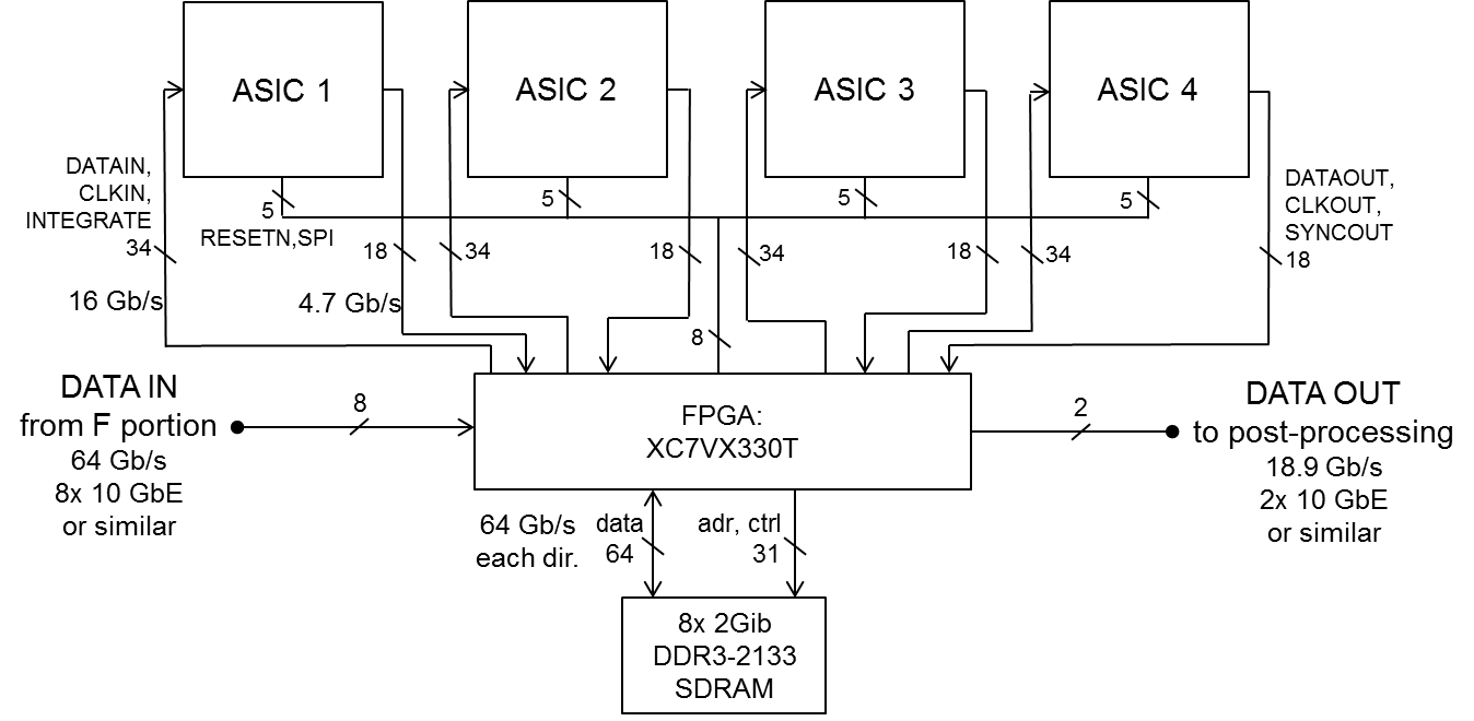
The FPGA provides 8 high-speed serial ports (8 Gb/s each) for receiving the input data for all the correlation ICs, and 2 similar ports for transmitting the output data. The data could be organized into 10 Gb/s Ethernet frames or into any of various other standard protocols.
From Table 5, each IC’s power dissipation is 1.82 W. The FPGA is estimated to dissipate 5.55 W Xilinx (2012), and the memory chips (8 at 8x256K) 3.7 W Micron (2011), giving 16.5 W of dissipation per board for signal-processing devices. Allowing 20% for power supplies and other overhead then gives 19.8 W per board. The system requires 128 boards, resulting in a total X-portion dissipation of 2.54 kW. The system-level energy figure of merit is then 4.84 pJ per CMAC operation.
This example uses 28-nm FPGAs and DDR3 memory devices that are readily available now. More advanced devices of both types are becoming available [including 20 nm and eventually 14 nm FPGAs Merrit (2013), and Hybrid Memory Cubes HMC Consortium (2014)]. Use of these would decrease the power for supporting devices and allow more correlation ICs per board, resulting in a system-level power efficiency approaching that of the correlation chips.
7 Conclusions
The IC design presented here provides a power-efficient means of computing all cross-correlations among many signals. The power efficiency is more than two orders of magnitude better than that of existing large correlators, and about a factor of 10 better than planned correlators based on future-generation FPGAs. The IC is flexible, in that it can be used to construct correlators for almost any number of antennas and any bandwidth, although its efficiency is best if is a multiple of 64.
The design has been synthesized and subjected to careful post-synthesis simulation and analysis. From this we know that it will be smaller than 12 mm2 when fabricated in the IBM 32SOI process, and we have accurate estimates of its power consumption. However, the physical design (detailed layout) has not yet been done and devices have not yet been fabricated.
In the radio astronomy community, there is currently a strong preference for building correlators from off-the-shelf programmable components like FPGAs and GPUs. So far, those devices have been used only for relatively small correlators. Technology advances through Moore’s Law continue to increase the size of digital processing machines that can be built that way, but custom-designed devices also benefit from these advances. The argument is sometimes made that when faced with requirements that cannot be reasonably met by today’s off-the-shelf devices, it is better to wait a few years until the devices get better than to spend that time developing a custom device. The results presented here belie that argument. We can do much better with devices fabricated in a technology that has been available for 5 years (32 nm) than with FPGAs that are two generations more advanced (14-16 nm) and not yet available.
The development cost of an ASIC is sometimes a deterrent to its adoption. For the large telescopes now planned or underway, it is a negligible fraction of the total development cost and is recoverable by energy cost savings in the first few years of operation. For smaller projects, several may be able to share the up-front costs provided that the design is flexible enough to be used in all of them. For our design, a substantial part of the development work has already been done.
The design presented here would be a good choice for telescopes whose designs will be frozen in the next few years. For correlators needed further in the future, it would be reasonable to port the design to a more advanced technology, such as the 14 nm finFET processes that are now becoming available. In such a next-generation design, other improvements could be considered, such as adding high-speed serial I/O (currently feasible but cost-prohibitive) and increasing the sizes of the CMAC array and memory.
Acknowledgments
This work was carried out at the Jet Propulsion Laboratory, California Institute of Technology, under a contract with the National Aeronautics and Space Administration and funded through the internal Research and Technology Development program.
We thank Dayton Jones, Joseph Lazio and Sander Weinreb of JPL/Caltech for advice and encouragement throught this project. Jim Maryoung of Synopsys Inc. provided an exceptional level of assistance in the use of his company’s tools. David Hawkins, Jonathon Kocz, and Sander Weinreb provided valuable comments on an early draft.
Appendix A: Clock Tree Synthesis
Here we describe a manual, non-optimum synthesis of the clock trees for the purpose of estimating their power and area. Final design of clock trees will be done during layout.
Two library cells were selected for building the trees, and their main properties are given in Table Appendix A: Clock Tree Synthesis. Both are from the high-threshold-voltage library. {wstable}[h] Library Data on Standard Cells Used for Clock Tree Buffers \toprulecell name input cap. intrinsic delay delay/load leakage pwr internal energy area fF ps ps/fF W fJ \colruleBUF_X16M 3.80112 14.61741 0.17408 0.022023 10.410215 2.691 INV_X9M 6.55092 2.71712 0.58739 0.009357 2.49423 1.287 \botrule We adopt the constraint that the delay through the tree should be less than 20% of the clock period, and we use the maximum clock rate of each net (500 MHz for INCLK and 360 MHz for sysclk and CLK_CMAC). This gives maximum delays of 400 ps for INCLK and 555 ps for sysclk and CLK_CMAC.
To determine the delay, we adopt the rule-of-thumb that the wire load on a net is 2 fF for each destination cell input1414 14 This is justified by experience with this design. Neglecting I/O cells and clock trees, the total switching power with Design Compiler Topographic’s estimate of the wire load is 152.3 mW (Table 4.1). The corresponding value with no wire load, using the synthesized netlist and delays from a compiler run with ideal wires (no capacitance and no delay) is 78.4 mW. There are other differences between these synthesized designs, but this indicates that, on average, the total load is about twice the destination pin load. Since the average input pin load throughout the design is about 1.9 fF, we adopt a conservative estimate of 2 fF of wire load per destination cell., and we neglect the network delay because the chip is small (about 3.4 mm edge-to-edge, giving a network delay of about 19 ps at a dielectric constant of 2.7). The selection of the two standard cells in Table Appendix A: Clock Tree Synthesis was made by considering various pairs of possible buffer cells and finding the maximum number of one that can be driven by the other while keeping the delay sufficiently low. From this we find that three levels of buffering are needed for the CLK_CMAC network (311,488 loads), but two are sufficient for sysclk and INCLK. The buffer trees constructed from these cells will certainly not be optimum, but we are not attempting to produce the optimum design in this simple exercise; we merely want to produce a feasible design and evaluate its area and power. It will then be apparent whether further optimization is worthwhile.
Since these are all clock nets, the final destination loads are the clock pins of flip flops. There are 6 types of D FF in the library, and each has versions with 3 or 4 drive strengths, but among all of them the clock pin capacitance ranges from 0.499 pF to 0.672 pF. The maximum capacitance was used for our delay calculations.
From the above considerations, we choose the following rough designs: CLK_CMAC, 311488 loads: 2686x INV_X9M fanout 116, driving the destination loads 75x INV_X9M fanout 36, driving above buffers 1x BUF_X16M fanout 75, driving above buffers. sysclk, 8352 loads: 48x INV_X9M fanout 175, driving the destination loads 1x INV_X9M fanout 48, driving the above buffers. INCLK, 3168 loads: 26x INV_X9M fanout 125, driving the destination loads 1x INV_X9M fanout 26, driving the above buffers. Using these designs and the data of Table Appendix A: Clock Tree Synthesis, Table Appendix A: Clock Tree Synthesis shows the results of calculating the area, power, and delay of the three buffer trees. The frequency of each clock is the effective frequency in the scenario that was simulated in Section 4.2, not the maximum used for timing. The switching power of nets driving the destination cells was already included in the Power Compiler results (Table 4.1), so it is excluded from the “added power” in Table Appendix A: Clock Tree Synthesis. The total power added by these buffer trees is then about 39.65 mW. Optimized buffer trees will use less. The added cell area is 3654 . The calculated delay through each buffer tree is also given, showing that each is less than the limit we specified. {wstable}[h] Calculation of Power and Area for Clock Buffer Trees \topruleNet CLK_CMAC sysclk INCLK Totals Max. freq.a, MHz 360 360 500 Frequencyb, MHz 62.5 227.273 500 Cell INV_X9M INV_X9M BUF_X16M INV_X9M INV_X9M INV_X9M INV_X9M Number 2686 75 1 48 1 26 1 Fanout per cell 116 36 75 175 48 125 26 Load per cell, fF 309.953 307.833 641.319 467.601 410.444 334.001 222.324 Leakage, W 25.13 0.70 0.02 0.45 0.01 0.24 0.01 26.57 Internal, W 837.44 23.38 1.30 54.42 1.13 64.85 2.49 985.02 Switching, W 42146.98 1168.80 32.47 4131.90 75.56 3517.03 90.04 51162.78 Delay, ps 184.7793 183.5343 126.2569 277.3799 243.8067 198.9048 133.3073 Total power, W 44236.23 4263.47 3674.67 52174.36 Load pin sw., W 10599.91 1039.17 884.53 Added power, W 33636.32 3224.30 2790.14 39650.76 Total delay, ps 494.5705 521.1866 332.2121 Total cell area, 3556.0980 63.0630 34.7490 3653.9100 \botrule
- a
Maximum switching frequency, for delay constraint.
- b
Effective switching frequency in the simulated scenario, for power calculation.
References
- Altera (2015) Altera Corp. [2015], Stratix V Device Data Sheet. Available at: http://wl.altera.com/literature/hb/stratix-v/stx5_53001.pdf .
- ARM (2015) ARM, Inc. [2015], Standard cell logic libraries for IBM 32SOI process: http://www.arm.com/products/physical-ip/index.php.
- Baudry & Webber (2011) Baudry, A. and Webber, J. [2000], “The ALMA 64-antenna correlator: Main technical features and science modes.” XXXth URSI General Assembly and Scientific Symposium, Istanbul, 13–20 Aug. 2011.
- Bunton (2015) Bunton, J. [2015], private communication (email of 2015 September 14, “Correlator power estimates”).
- Carlson (2015) Carlson, B. [2015], private communication (email of 2015 September 21, “correlator power estimates”).
- D’Addario et al. (1984) D’Addario, L. R., Thompson, A. R., Schwab, F. R., and Granlund, J. [1984], “Complex Cross Correlators with Three-Level Quantization: Design Tolerances.” Radio Science 19, 931–945.
- D’Addario (2011) D’Addario, L. R. [2011], “Low-Power Correlator Architecture For the Mid-Frequency SKA,” SKA Memo 133, 2011 March 21. Available at http://www.skatelescope.org/memos.
- D’Addario (2015a) D’Addario, L. R. [2015a], “Overflow and Underflow.” Correlator ASIC Memo No. 11, 2015 January 21. JPL internal report, available from the author by request.
- D’Addario (2015b) D’Addario, L. R. [2015b], “Correlator Unit With External Memories.” Correlator ASIC Memo No. 12, 2015 January 14. JPL internal report, available from the author by request.
- D’Addario (2015c) D’Addario, L. R. [2015c], “Correlator ASIC Power Analysis, Part 2.” Correlator ASIC Memo No. 14, 2015 July 31. JPL internal report, available from the author by request.
- Denman et al. (2015) Denman, N., Amiri, M., Bandura, K., et al., “A GPU-based correlator X-engine implemented on the CHIME Pathfinder.” IEEE 26th International Conference on Application-specific Systems Architectures and Processors (ASAP), Toronto, 27-29 July 2015, pp 35–40.
- Elenius & Levine (2000) Elenius, P., and Levine, L. [2000], “Comparing Flip-Chip and Wire-Bond Interconnection Technologies.” Chip Scale Review, 4, 6 (July/August 2000). Available at: http://processsolutionsconsulting.com/pdf/Flip_Bump/csr-7-00.pdf.
- HMC Consortium (2014) HMC Consortium [2014], Hybrid Memory Cube Specification 2.0. Nov. 2014. Available at: www.hybridmemorycube.org.
- IBM (2009) IBM Corp. [2009], “IBM Announces Industry’s Densest, Fastest On-Chip Dynamic Memory in 32-Nanometer, Silicon-on-Insulator Technology.” News release dated 18 Sep 2009. Available at: https://www-03.ibm.com/press/us/en/pressrelease/28428.wss .
- IEEE (2001) IEEE Computer Soc. [2001], 1497-2001—IEEE Standard for Standard Delay Format (SDF) for the Electronic Design Process. IEEE Std 1497-2001, DOI: 10.1109/IEEESTD.2001.93359, latest version dated 06 Aug 2002.
- Kocz et al. (2015) Kocz, J., Greenhill, L. J., Barsdell, B. R., et al. [2015], “Digital Signal Processing Using Stream High Performance Computing: A 512-Input Broadband Correlator for Radio Astronomy.” J. of Astronomical Instrumentation, 4, 1550003.
- Mahdy (1999) Mahdy, Y. B. [1999], “Algorithm and Two Efficient Implementations for Complex Multiplier.” Proceedings of ICECS ’99, vol. 2, pp 949–952.
- McKinnen (2010) McKinnen, M. [2010], private communication (email of 2010 Feb 11, “EVLA correlator power”).
- Mentor Graphics (2015) Mentor Graphics, Inc. [2015], ModelSim simulation software. http://www.mentor.com/products/fv/modelsim/ .
- Merrit (2013) Merrit, R. [2013], “Intel to make 14-nm FPGAs for Altera.” EE Times (on-line newsletter), 26 Feb. 2013.
- Micron (2011) Micron Corp. [2011], “DDR3 SDRAM System Power Calculator.” Spreadsheet, revision 0.96, July 27, 2011. Available at http://www.micron.com/support/power-calc .
- Morales (2011) Morales, M. [2011], “Enabling Next-Generation Dark Energy and Epoch of Reionization Radio Observatories with the MOFF Correlator.” Pub. Astronon. Soc. of the Pacific, vol. 123, No. 909, pp. 1265–1272.
- Motorola (2003) Mortola, Inc. [2003], SPI Block Guide V03.06. Doc. No. S12SPIV3/D, revised 04 Feb. 2003. Available at: www.ee.nmt.edu/t̃eare/ee308l/datasheets/S12SPIV3.pdf. See also http://www.byteparadigm.com/applications/introduction-to-i2c-and-spi-protocols.
- Nagel & Pederson (1973) Nagel, L. W. and Pederson, D. O. [1973], “SPICE (Simulation Program with Integrated Circuit Emphasis).” Memorandum No. ERL-M382, University of California, Berkeley, April 1973. Current version available as open-source software at http://bwrcs.eecs.berkeley.edu/Classes/IcBook/SPICE/ .
- Perley et al. (2009) Perley, R., Napier, P., et al. [2011], “The Expanded Very Large Array.” Proc. IEEE, 97, 1448–1462.
- Synopsys (2015) Synopsys, Inc. [2015], “DC Ultra: Concurrent Timing, Area, Power, and Test Optimization.” Design Compiler Ultra datasheet. Available at: http://www.synopsys.com/Tools/Implementation/RTLSynthesis/DCUltra/Documents/DCUltra-ds.pdf .
- Tegmark (2009) Tegmark, M. and Zaldarriaga, M. [2009], “The Fast Fourier Transform Telescope.” Phys. Rev. D, 79, 083530.
- Thompson et al. (2001) Thompson, A. R., Moran, J. M., and Swenson G. W. Jr. [2001], Interferometry and Synthesis in Radio Astronomy. 2nd ed., John Wiley & Sons, New York.
- Xilinx (2012) Xilinx Corp. [2012], “XPower Estimator (XPE)—14.1.” Xilinx Power Estimator spreadsheet for 7-series devices, released 8 May 2012. Current version available at http://www.xilinx.com/products/technology/power/xpe.html.
- Van Vleck & Middleton (1966) Van Vleck, J. H., and Middleton, D. [1966], “The Spectrum of Clipped Noise.” Proc. IEEE 54, 2–19.
- Wooten & Thompson (2009) Wooten, A., and Thompson, A. R. [2009], “The Atacama Large Millimeter/Submillimeter Array.” Proc. IEEE, 97, 1463–1471.