Effect of Jitter on the Settling Time of Mesochronous Clock Retiming Circuits
Abstract
It is well known that timing jitter can degrade the bit error rate (BER) of receivers that recover the clock from input data. However, timing jitter can also result in an indefinite increase in the settling time of clock recovery circuits, particularly in low swing mesochronous systems. Mesochronous clock retiming circuits are required in repeaterless low swing on-chip interconnects. We first discuss how timing jitter can result in a large increase in the settling time of the clock recovery circuit. Next, the circuit is modelled as a Markov chain with absorbing states. The mean time to absorption of the Markov chain, which represents the mean settling time of the circuit, is determined. The model is validated through behavioural simulations of the circuit, the results of which match well with the model predictions. We consider circuits with (i) data dependent jitter, (ii) random jitter, and (iii) combination of both of them. We show that a mismatch between the strengths of up and down corrections of the retiming can reduce the settling time. In particular, a 10% mismatch can reduce the mean settling time by up to 40%. We leverage this fact toward improving the settling time performance, and propose useful techniques based on biased training sequences and mismatched charge pumps. We also present a coarse+fine clock retiming circuit, which can operate in coarse first mode, to reduce the settling time substantially. These fast settling retiming circuits are verified with circuit simulations.
Index Terms:
Settling time, clock recovery, metastability, inter-symbol interference, low swing interconnect, absorbing Markov chains.I Introduction
Timing jitter in the incoming data degrades the bit error rate (BER) of receivers that recover clock from the data itself, and this effect has been extensively studied (c.f., [1, 2]). However, it has been recently observed in [3] that, under certain conditions, timing jitter can also increase the settling time of clock retiming circuits. In this paper, we present a detailed analysis of the settling time of mesochronous clock retiming circuits in the presence of jitter.
Mesochronous clock retiming circuits are required in repeaterless low swing on-chip interconnects to sample the data correctly at the receiver [4, 5], and also in off-chip links that use a forwarded clock [6, 7]. In mesochronous receivers, a clock running at the correct frequency is available at the receiver and only the correct phase needs to be recovered. Hence, such clock retiming circuits use delay line [5, 4] or phase interpolators [8] to generate the required clock phase. Use of delay based retiming circuits is preferred over systems that use phase locked loops with a voltage controlled oscillator (VCO) per channel due to their better performance and lower complexity [9]. Delay based retiming circuits are preferred even in systems where the clock frequency is known only nominally and not exactly [8]. Fast locking clock data recovery (CDR) circuits (also known as burst mode CDRs [10]) offer very short settling times. These CDR circuits use gated VCOs [11], oversampling [10] or injection locking [12]. However, these CDR circuits have certain limitations. Gated VCOs have poor phase aligning and no input jitter rejection. Oversampling CDRs come with high complexity and power consumption. Injection locked CDRs have quantization phase error and high cycle to cycle jitter. Hence, for source synchronous on-chip and chip to chip links, delay based retiming circuits are preferred. Hsieh et al., in [13], provide a detailed discussion and comparison of different CDR circuit architectures.
Delay based clock retiming circuits are known to offer fast settling times as compared to PLL based synchronizers as they do not need a clock synthesis step [13]. Timing jitter can increase the settling time of such delay based clock retiming circuits indefinitely[3]. This occurs when the circuit wakes up with its clock in the horizontally closed region of the data eye. Typical systems implemented on-chip can have hundreds of long interconnects [14, 15], and a horizontal eye opening of about 85% is not pessimistic [16, 17]. If the initial clock position is assumed to be uniformly distributed, there is a 15% chance that the circuit wakes up with its initial clock phase in the closed region of the eye, making it important to study and understand this problem. To analyze the settling time, the clock retiming circuit can be modelled as a Markov chain with absorbing states [3]. Here the states correspond to the clock positions. The state transitions correspond to the phase corrections done by the clock recovery circuit. This model provides useful insights into the dynamics of the system. In particular, as shown in this work, the mean settling time of the circuit is predicted by the model.
In this paper, we investigate the settling time of mesochronous clock retiming circuits in detail. Section II presents a detailed discussion on the settling time of mesochronous clock retiming circuits, in particular, its dependence on timing jitter, which is the main focus of this work. We demonstrate the increase in settling time, caused due to jitter, using experiments performed on a chip and these experiments are described in Section III. Next, toward analyzing different types of jitter, a Markov chain model of the mesochronous synchronizers is presented in Section IV. As the settling time is random, it cannot be determined exactly. However, using the Markov chain model we can determine bounds on the settling time. These are given in Section V. Techniques for reducing the settling time, along with supporting circuit simulations, are given in Section VI. Finally, we make overall concluding remarks in Section VII.
II Settling time of the clock retiming circuit
In order to analyze the settling time of a mesochronous system, we consider a repeaterless interconnect system as shown in Fig. 1. Here the delay of the interconnect is expressed as , where , and is the system clock period.

and are the phases of the transmitter and receiver clocks respectively. The clock retiming circuit derives the sampling clock , which is positioned at the center of the input data eye, from the receiver clock phase. The settling time of the circuit is defined as the time it takes the circuit to derive this sampling clock phase. This time depends on the initial phase error between the clock and the data. This initial phase error is a continuous variable taking values in . When the initial phase error is less than , the circuit achieves lock by decreasing the phase to 0. On the other hand, when is greater than , the circuit achieves lock by increasing the phase difference to , which is the same as 0 by phase wrapping (refer Fig. 2).

The settling time of the clock recovery circuit depends on the gain of the system and the initial phase error. For mesochronous systems, this settling time can be expressed as
| (1) |
Here is the loop filter capacitor, is the gain of the phase modulator, is the gain of the charge pump and is the data activity factor. The expression in (1) is derived in Appendix A.
II-A Lengthening of the settling time
When the initial phase difference is equal to , the circuit can settle at two discrete values of the phase difference: or (which is same as by phase wrapping), and both the solutions are acceptable. Since the initial phase difference is a continuous variable, the above scenario is one of taking a discrete decision on a continuous input. Theoretically, such decisions can take an infinite amount of time for certain initial conditions [18]. This happens when is exactly radians and the system has no reason to choose one solution over another. This is akin to metastability in flip-flops [19]. When is exactly radians, the flip flops in the phase detector become metastable. In these conditions, the phase detector loop enters a state of indecision. However, for sustained indecision of the phase detector loop, the flip-flops in the phase detector must become metastable in every clock cycle. Practically, however, given the narrow widths of the metastability windows, the fast recovery times and the inherent jitter present in the clocks, sustained loop indecision due to flip-flop metastability is highly unlikely. Hence, metastability of the flip-flops in the phase detector is not discussed in this work.
II-B Effect of timing jitter: The window of susceptibility
When the input data has timing jitter (due to inter-symbol-interference (ISI) in the data and/or random jitter in the clock) and the initial clock phase () is in the horizontally closed region of the data eye, the expression of settling time in (1) is not valid. Fig. 3 illustrates an eye diagram with timing jitter and when is in the horizontally closed region of the data eye.

This region is called the window of susceptibility () henceforth. When the initial clock is in this window the output of the phase detector is randomized by the jitter in the data, and hence, the phase error information is lost. This increases the settling time indefinitely, till the system escapes this window .
II-C Working of phase detectors in the window of susceptibility


The phase detector takes 2 samples per bit period and takes a binary decision of shifting the clock to the right or to the left based on the last three samples (labeled as A, B and C in Fig. 4). When there is no jitter in the data, the phase detector consistently produces either up (UP) or down (DN) pulses. Thus, for a given data activity factor , the settling time can be calculated using (1).
The phase detector’s decision to assert one of UP or DN signals depends on the value of the sample taken at time instant B. Fig. 4 shows the timing diagram of the Alexander phase detector when the data is corrupt with timing jitter and the initial phase error is close to radians, i.e., the initial clock position is in the window [3]. Due to jitter the value of the sample at time instant B depends on the current data transition time and not on the average data arrival time. Hence, the phase detector produces UP and DN pulses randomly and the clock recovery circuit can remain stuck, with its clock in this region, indefinitely.
Linear phase detectors like the Hogge phase detector [21] behave similar to binary phase detectors in the window of susceptibility. The ideal characteristics of the Alexander and Hogge phase detectors are shown in Fig. 5. The highlighted region shows the window , and within this window the variation in the gain of the phase detector is negligible. Hence, the analysis of the system behaviour in the window is applicable to both these types of phase detectors.

The width of the window () depends on the amount of timing jitter present in the system and the threshold of the sampling comparators. The effect of offset on is illustrated in Fig. 6.

To understand the effect of the offset, let us consider the case when there is an offset and the initial clock position at as shown in Fig. 6. Here we consider the scenario when there is non-zero offset, and the initial clock position is outside the window of susceptibility as shown in Fig. 6. Here, for every transition, the circuit makes a correction by shifting the clock to the left. Similarly, for every transition, the circuit makes a correction by shifting the clock to the right. Since every transition is followed by a transition, the net result is that the clock remains stuck. Hence, as shown in Fig. 6, offsets can result in increasing the width of the window of susceptibility . We will revisit this with the example of offset in the presence of 1-bit ISI in Section IV-A1.
III Experimental demonstration of the increase in settling time
We use the coarse+fine retiming circuit for on-chip interconnects reported in [5] for the analysis and experiments. Fig. 7 shows the block diagram of this synchronizer.

In this circuit, a delay locked loop (DLL) is used to generate multiple phases of the clock. A controller picks one of the phases of the DLL and delays it to bring the output clock to the center of the eye using a voltage controlled delay line (VCDL). The controller comprises a phase detector which senses the phase difference between the clock and the data and integrates the error using a charge pump. This charge pump is called the weak charge pump. The integrated error voltage is used to control the delay of the VCDL. If the VCDL range is not sufficient to achieve lock (which is detected by the control voltage exceeding preset upper and lower voltage bounds and ), the controller automatically picks the next adjacent phase, resets the control voltage using a strong charge pump and re-attempts to lock. The process repeats till lock is achieved.
Most of the circuit blocks used in the clock retiming circuit in Fig. 7 are standard circuit elements, except for the charge pump circuit which consists of the weak and the strong charge pumps. Fig. 8 shows the transistor level circuit diagram of the weak and strong charge pumps.

When the control voltage is outside the bounds and , the strong charge pump is activated which brings the control voltage within the bounds. During this period, when the strong charge pump is active, the weak charge pump is disabled by the transistors and as shown in Fig. 8.
We have measured the lengthening of the settling time on a prototype chip of this synchronizer. The chip has a circuit with a low swing transmitter and an interconnect which produces some ISI. Fig. 9 shows the simulated eye diagram at the receiver for a clock frequency of 2 GHz.

The chip was tested at a frequency of 2 GHz with Centellax TG1B1-A data generator [22] and Centellax TG1C1-A clock synthesizer [23]. In the clock synthesizer instrument, one of the clock outputs can be phase shifted with a resolution , which is used for programming the initial phase error. Fig. 10 shows the control voltage evolution when the circuit is stuck in the horizontally closed region of the eye at startup.

Notice the abrupt change in the slope of the signal when the circuit escapes the window , which happens after about 725 cycles in this example. When the circuit is initialized at the edge of this window, such a lengthening of settling time is not observed as shown in Fig. 11.

The lengthening of the settling time was observed with different data patterns like PRBS7, PRBS15 and PRBS31. In addition, the TG1B1-A data generator produces outputs with different Mark-to-Space ratios. The Mark-to-Space ratios can be chosen between , and . Even with these different patterns, the increase in settling time occurs when the clock is initialized in the closed region of the data eye. Fig. 12 shows the control voltage evolution when the circuit is stuck in the horizontally closed region of the eye with a data pattern with Mark-to-Space ratio of , in which case the circuit remains stuck with its clock in the window for about 1200 cycles.

As expected the total settling time is higher for a lower data activity factor. It is worth noting that changing the Mark-to-Space ratio only changes the data activity factor. The minimum run length for logic 1 and logic 0 is still 1-bit. We will show in Section VI that by changing the minimum run length for one of the logic levels, the settling time can be reduced considerably.
Having demonstrated the problem of increased settling time, the next section will analyze the settling time of these circuits in the presence of different types of jitter.
IV Markov chain model of the clock recovery circuit
In order to analyze the settling time when the initial clock is in the window , the circuit is modelled as a Markov chain with absorbing states [24]. The binary phase detector produces UP or DN pulses on every data transition, which are converted into an analog control voltage using a charge pump. The control voltage is used to delay the clock (either using a phase interpolator or a delay line). Since the input is binary, the output phase is quantized. Hence, the clock position can be discretized to the step size () of the phase detector loop update. In order to keep the jitter in the recovered clock low, controllers typically use step sizes of less than 0.1% of the clock period (c.f., [5, 8, 25, 26]). The region where the input data eye is closed, i.e., the window is of particular interest. A Markov chain model of the system is constructed in which the states designate the clock positions and the phase corrections performed by the clock retiming circuit form its state transitions. The edges of the window are modelled as absorbing states.
The sources of timing jitter are data dependent jitter (ISI induced) in the data and noise induced random jitter in the clocks of
the transmitter and receiver. The analysis for each type of jitter is
done separately, followed by an analysis for data dependent and random
jitter together. For analyzing the effect of data dependent jitter, an
interconnect link with different bandwidths is considered. The
interconnect is modelled as a 20 section RC network. For simulating
different amounts of ISI, different values of RC time constants are
chosen and the eye diagrams and timing jitter histograms for a few
considered channel bandwidths are listed as cases 1 through 3 as
follows:
- Case 1
-
For benign channels the horizontal eye opening approaches 100% and the jitter histogram has a narrow distribution as shown in Fig. 13.

Fig. 13: Eye diagram and zero crossing histogram for a benign channel. - Case 2
-
As the bandwidth of the channel decreases, the jitter histogram splits and produces two distinct peaks [27]. This shows that the ISI due to the immediate previous bit is dominant (Fig. 14).

Fig. 14: Eye diagram and zero crossing histogram for a channel for which the ISI due to the immediate previous bit is dominant. - Case 3
-
Further reduction in the bandwidth shows that the jitter histogram splits into 4 regions as shown in Fig. 15. This shows that the ISI due to previous two bits is dominant.

Fig. 15: Eye diagram and zero crossing histogram for a channel for which the ISI due to previous 2 bits is dominant.
Further reduction in the bandwidth of the channel results in the jitter histogram splitting to 8 peaks, 16 peaks and so on [27]. While the modeling presented in this paper can be used to analyze these scenarios, such channels are not usable due to the very high ISI present. Hence, our analysis considers ISI of 1 previous bit and 2 previous bits. For modeling effect of random jitter, the random jitter is assumed to have a Gaussian distribution [28]. Overall, the system is analyzed for the cases when the jitter is
- 1.
induced by ISI due to 1 previous bit,
- 2.
induced by ISI due to 2 previous bits,
- 3.
random with a Gaussian distribution and
- 4.
induced by random jitter and ISI due to 1 previous bit.
IV-A Markov chain model for jitter induced by 1 bit ISI
When the ISI due to the immediate previous bit is dominant, the zero crossings of the data are bunched into two narrow distributions as shown in Fig. 14. This is approximated to the data signal following one of two distinct traces. Fig. 16 illustrates an eye diagram with ISI due to exactly 1 previous bit.

Here is the initial sampling instant of the clock, is the distance to the right edge of the window and is the threshold of the samplers in the phase detector. and represent the two distinct zero crossing times of the data signal. For the eye diagram shown in Fig. 14, the size of the window is about 4% of the bit period. This means is about . Assuming that the source outputs 1 and 0 with equal probability, the bit combinations that result in traces with zero crossing at and , respectively, are listed in Table I. Here is the current bit corrupt with ISI due to immediately previous bit . A data transition occurs when . Table I lists all 3 bit combinations which cover all possible data traces.
| Zero crossing time | Action | |||
| 0 | 0 | 0 | - | |
| 0 | 0 | 1 | ||
| 0 | 1 | 0 | ||
| 0 | 1 | 1 | - | |
| 1 | 0 | 0 | - | |
| 1 | 0 | 1 | ||
| 1 | 1 | 0 | ||
| 1 | 1 | 1 | - |
Here and indicate that the clock is shifted to the left and to the right, respectively, by a step of size while indicates no corrective action in that cycle. When all sequences are equally likely, the probabilities and . Note that the system escapes the window of susceptibility when, for the first time, either or . Here and are the total number of times the clock position has been shifted to the right and to the left, respectively, from start-up.
This system is modelled as a one dimensional Markov chain. The states of the Markov chain correspond to the positions of the sampling clock in the window Once the clock escapes this window, the time taken to lock to the center of the eye can be calculated from (1). Thus, the edge positions of the window are modelled as absorbing states, thereby making this a Markov chain with absorbing states [24]. Fig. 17 shows the state diagram of the Markov chain for this system.

By knowing the state space and the transition probabilities of a Markov chain, one can calculate the mean time to absorption from any initial state [24]. The calculation of the mean time to absorption (and its variance) is presented in Appendix B.
The combined plots of the mean settling time for the 1 bit ISI case obtained from behavioural simulations of the circuit and its Markov chain model predictions via the mean absorption time are shown in Fig. 18.

The behavioural simulations were done using a 20 section RC interconnect and a VerilogA behavioural description of the clock retiming circuit, while the model predictions were computed by solving for the mean absorption time of this Markov chain using a linear equation solver.
As one would expect, the settling time is maximum when the initial sampling phase is at the center of the window It is worth noting that the variance of the absorption time is quite high. Fig. 19 shows the standard deviation of the absorption time as predicted by the Markov chain model and as observed in the data obtained from behavioural simulations.

IV-A1 Modeling the effect of offset and 1-bit ISI
As was discussed in Section II, offsets can increase the width of the window of susceptibility. Fig. 20 illustrates an example of the effect of offset in the case when the ISI is limited to 1 previous bit.

In this case, the circuit behaviour crucially depends on the clock position in the window. In particular, it differs when the clock is in , and in . For instance, using a procedure similar to the one described for analyzing 1-bit ISI, one can easily verify that the probabilities for left and right shifts are as follows.
| Window | |||
|---|---|---|---|
| 0.375 | 0.125 | 0.5 | |
| 0.25 | 0.25 | 0.5 | |
| 0.125 | 0.375 | 0.5 |
By constructing the Markov chain with above transition probabilities, the settling time analysis can be extended to analyze the effect of any given offset in a straightforward manner.
IV-B Markov chain model for jitter induced by 2 bits ISI
When the ISI due to previous two bits is significant, the data transitions histogram has 4 peaks as shown in Fig. 15. This can be approximated to ISI of exactly two bits which results in 4 distinct data transition times. Fig. 21 illustrates an eye diagram when ISI is limited to two bits and the four data transition times are labeled as , , and .

Thus, the window of susceptibility can be divided in to three sub-windows which are , and . Unlike the 1 bit ISI case, the occurrences of the traces with zero crossing time at , , and are not independent of each other. Thus, the system is no longer memoryless, and hence, requires a second order Markov chain model. A second order Markov chain model is, in general, difficult to analyze. A technique to convert this second order Markov chain to a first order Markov chain (with an enlarged state space) is described in the following. This greatly simplifies the analysis, as known results for first order Markov chains can be directly applied.
To construct the Markov chain model of the system, one needs to first consider the order of occurrences of the traces with zero crossing times at , , and . Fig. 22 shows the state diagram of the source data.
The finite state machine (FSM) is limited to 3 bit combinations as the ISI for every bit is limited to previous two bits. The state transitions are labeled with the zero crossing locations of the data signal through . , , indicates a state transition without a data transition.
The second order Markov chain model for this system is shown in Fig. 23. To capture the memory of the system, six states are used for each clock position. Four of these states correspond to the previous data transition () occurring at , , and . The remaining two states are i) which indicates no data transition in the previous cycle, and ii) which indicates no data transition in the previous two cycles.
For example, when , the source can be in either state or (refer Fig. 22) and the next cycle will either not have a data transition or have a data transition at position . When the initial clock is in the sub-window , a data transition at results in a clock shift to the right by 1. Thus, the transitions from state at are either to state at the same clock position or to state of the next clock position to the right. Extending the analysis to the rest of the FSM in Fig. 22, the rest of the state transitions can be determined. In Fig. 23, the transitions are shown for only one clock position for brevity, in particular, for the clock positions in the sub-window . Note that all the state transitions have a probability of 0.5 when the data source outputs 0 and 1 with equal probability.
Similar to the 1 bit ISI case, the mean time to absorption for the 2 bit ISI case was determined using the Markov chain model. Also, behavioural simulations were performed. For the eye diagram shown in Fig. 15, the window size is about 30% of the clock period. Here , , and . The mean time to absorption for each clock position was taken as the average of the mean times to absorption from each of the six states in the Markov chain that correspond to that position. For the behavioural simulations, a 20 section RC interconnect was used with a VerilogA behavioural description of the clock retiming circuit. In order to reduce the simulation time and the required sample size, a step size of 3.5 was used for this analysis. The combined plots of the mean time to absorption for 2 bit ISI case obtained from behavioural simulations and Markov chain model predictions are shown in Fig. 24.

The behavioural simulations used an RC circuit for the interconnect, whereas the Markov chain model truncated the ISI to 2 bits. Note that the peak of the mean time to absorption, as predicted by the model, is about 1100 cycles when the step size is 3.5. This can be as high as 12000 cycles when the step size is 1.
Thus, we can conclude that the predictions of the settling time of the clock retiming circuits by the Markov chain model have good accuracy. The Markov chain model predictions are presented for an equiprobable bit sequence as the data. As seen in Fig. 24, these predictions differ slightly from those given by the behavioural simulations, where the latter are performed for a bit sequence generated by the random number generator in VerilogA. The deviation is owing to the following: i) the random bit sequence generated is not exactly equiprobable, ii) a finite number of simulations are used.
IV-C Markov chain model for Gaussian distributed random jitter
This section discusses the increase in the settling time due to random jitter in the clock. There are two sources of clock jitter in digital systems: inherent jitter in the clock generating oscillator and jitter introduced by the clock distribution network. The former can be modelled as a Gaussian distribution [28]. The latter, however, depends on several factors and can be random with arbitrary distribution [29]. The analysis in this section assumes that the jitter has a Gaussian distribution.
For ease of analysis, it is assumed that the receiver clock is noise free and all the jitter is in the transmitter clock. This assumption is valid as long as the channel response is constant over the spectrum of the noisy clock. The jitter histogram is assumed to be a Gaussian distribution with a standard deviation of . The sampling clock position () with respect to the mean data transition position can be represented as , where is an integer taking values from to . Hence, with respect to the sampling clock position, the mean of the data transition can be written as . Unlike the analysis for ISI induced jitter where the window of susceptibility was bounded, random jitter may be unbounded, and hence, the size of the window may be arbitrarily large. For our analysis, a window size of , i.e., , is assumed. This covers of the possible data transition positions.
When the clock transition is to the right of the mean data transition position (), the circuit shifts the clock to the right towards final lock ( is incremented). However, even when , the random jitter in the data can cause the instantaneous data transition to occur to the right of the sampling clock position. This results in a clock shift in the wrong direction. Fig. 25 shows the probability distribution of the clock transition time and the data transition position.

The shaded area represents the probability that the data transition occurs to the right of the sampling clock position, when the mean of the data transition is to the left of the sampling clock transition (). This is the probability of a phase update in the wrong direction. This probability can be calculated as follows.
where is the standard complementary error function [24]. The probability of an update in the correct direction can then be calculated as
Note that these probability values will be scaled by a factor which equals the probability of transitions since the transitions occur independent of the clock jitter. For a source which outputs 1 and 0 with equal probability, the probability of transition is also . This equation is then used to construct the probability transition matrix of the Markov chain to predict the mean time to absorption and the standard deviation of the time to absorption. As noted earlier, absorption in this case is defined as the phase difference between the mean of data position and sampling clock position being . Fig. 26 shows the plots of the mean time to absorption and the standard deviation of the time to absorption with the initial clock position as estimated by the Markov chain model, when , i.e., standard deviation of the clock jitter is 2% of the clock period.

IV-D Modeling the effect of ISI and random jitter
The Markov chain model of the system can be easily extended to analyze the combined effect of data dependent and random jitter. An example case of jitter induced by 1 bit ISI and Gaussian distributed random jitter is shown in this section. When the jitter is solely due to 1 bit ISI, the data follows one of two distinct traces as discussed in Section IV-A. When random jitter is also present, the zero crossing of the data spreads around these two zero crossing positions. Since the random jitter is independent of the data, the probability distribution of the data zero crossing positions is equal to the product of the probability distribution of the zero crossing positions due to random jitter and due to 1 bit ISI. For the purpose of analysis it assumed that the receiver clock is jitter free and the transmitter clock has all the random jitter and the channel introduces data dependent jitter.
Fig. 27 shows the distribution of the data zero crossing positions and the sampling clock position when the data signal has both random jitter and 1 bit ISI induced jitter. The window of susceptibility is now widened to .

The effect of the data jitter can be modelled as a shift in the mean of the Gaussian random jitter. Hence, for random jitter along with jitter due to 1 bit ISI, the jitter at any time can be considered to be Gaussian distributed, with a standard deviation of and mean at either or . Consider an example clock position () as shown in Fig. 27. Choosing as the reference position for calculations, the probability of a data transition occurring to the left of the clock is given by
where is the cumulative distribution function (CDF) of a general Gaussian distribution with mean and standard deviation . The probability of a data transition to the right of the clock can then be calculated as
where is the probability of having no data transition in that clock cycle.
The Markov chain along with its transition probabilities was determined in this manner. Fig. 28 shows the mean absorption time and the standard deviation of the absorption time obtained for data with timing jitter induced by 1 bit ISI in addition to Gaussian distributed random jitter with standard deviation of 1% of the clock period.

V Bounds on the settling time
As the settling time is a random quantity, it is not possible to determine it exactly. However, in this section, we determine bounds on the settling time for a given value of probability of absorption, i.e., confidence level. Toward this we leverage the fact that the settling time of the circuit is maximum when the initial clock is at the center of the window of susceptibility (for a system without any programmed bias). In particular, the bound on the mean settling time will equal this maximum value of settling time.
Let be the row vector corresponding to the initial probability mass function on the states of the Markov chain. Here contains exactly one entry with value 1 which corresponds to the initial clock position (at the center of the window ), while the entries corresponding to the rest of positions are zeroes. Let the probability transition matrix of this Markov chain be denoted by . Using standard results for Markov chains [24], we know that given , the probability mass function on the states of the Markov chain after transitions is given by
For a Markov chain with absorbing states, the probability of absorption after transitions equals the sum of those entries of that correspond to the absorbing states. Hence, one can iteratively find the number of transitions required for absorption to occur for a given absorption confidence level (i.e., probability of absorption).
For illustrative purposes, we present results for a 1 bit ISI case with a window of susceptibility of size 40 steps. From the procedure described earlier to obtain a bound on the settling time, we now calculate the probability of absorption of the Markov chain as a function of the number of transitions. The results obtained are shown in Fig. 29.

In fact, this plot corresponds to the cumulative distribution function of the absorption time. Hence, it directly follows that the probability of absorption in exactly cycles corresponds to the slope of the above graph. This is shown in Fig. 30.

Observe that the distribution of probability of absorption is skewed as one would expect. The probability of absorption is zero for less than the distance to the nearest absorbing state. Also, for very large values of this probability approaches zero.
As seen from Fig. 29, for absorption with 99% surety, the Markov chain needs about 3000 state transitions. This number depends on the gain of the system and increasing the gain reduces the window size (in terms of number of phase steps), and hence, the settling time. An analysis of the number of transitions needed for absorption with 99% confidence with the size of the window, in terms of number of steps, was done. Fig. 31 shows the plot obtained from this analysis.

VI Techniques for reducing the settling time
VI-A The coarse first synchronizer
The settling time of the circuit depends on the loop gain or the step size of the phase correction circuit. A large step size will mean that the size of the window of susceptibility (in term of number of steps) is small. This results in quick settling, as was discussed in the previous section. However, a large step size results in high jitter in the clock after lock is achieved. The synchronizer proposed in [5] uses a coarse and a fine correction loop for accurate synchronization. The circuit designed there first tries to achieve lock using the fine tuning loop. If lock cannot be achieved in the limited range of the fine tuning loop, a coarse correction is initiated. If the fine tuning loop is disabled during the initial settling period, it enables us to have a much larger step size, and hence, a much faster settling. For instance, when a 10 phase DLL is used, and even if a horizontal eye opening of 50% is available, the size of is only 5 steps.
Fig. 32 shows the charge pump circuit for the synchronizer in Fig. 7, appropriately modified to have a coarse only mode.

Here, during the initial period after startup, a switch disconnects the loop filter capacitor and another set of switches convert the charge pump to a combinational circuit [30], i.e., connecting the gate of the PMOS current source to GND and gate of the NMOS current sink to VDD. This converts the current sources in the fine charge pump to ON switches. This essentially increases the current injected at every fine correction step, and the control voltage overshoots the bounds set by and in every cycle. Hence, the circuit takes a coarse correction step at every cycle of the divided clock. This is equivalent to disabling the fine tuning loop and ensuring a coarse tuning step in every cycle of the divided clock that drives the coarse tuning loop. After lock is achieved, the loop filter capacitor is connected back to the charge pump, and the gates of the PMOS current source and NMOS current sink are connected to and respectively, to resume normal operation.
The amount of time for which the coarse tuning loop should be run before enabling the fine tuning loop depends on the size of and on the desired confidence level for achieving lock within this period. In this example given in Fig. 7, the coarse synchronizer used a 10 phase (DLL). Assuming an extreme condition that the horizontal eye opening is only 50%, it means that the window size is 5 steps. From the analysis presented in the previous section, an absorption with 99% confidence level needs 32 cycles to be absorbed. This corresponds to 256 ns in absolute time if the coarse controller operates on a divide by 16 clock for a 2 GHz system clock.
The coarse first synchronizer was designed and simulated for a benign channel. The receiver input eye diagram for this test is shown in Fig. 33.

For an initial clock phase at the center of the settling behaviour is shown in Fig. 34.

As seen, the circuit escapes the window very fast and settles accurately once the fine tuning loop is enabled. The lower waveform is the select signal for switching from coarse mode to normal mode, which is run for 160 ns in coarse mode. This signal can be generated using a power on reset circuit.
This same synchronizer circuit was simulated with an input that had very high ISI. The receiver input eye diagram for this test is shown in Fig. 35.

With such data input, the settling of the synchronizer is shown in Fig. 36.

The clock was initialized to the center of the window . Even for this input, the circuit escapes the window within the coarse first operating period. The noise in the control voltage is primarily due to the high jitter in the incoming data.
VI-B Synchronizer with a bias towards one of the absorbing states
Reduction of settling time using the coarse first technique is specific to the coarse+fine type synchronizer in [5]. A different, though more general, technique of reducing the settling time is by introducing a mismatch in the relative strengths of the UP and DN updates in every cycle. Using the 1 bit ISI model for the purpose of illustration, we next discuss the settling time of this synchronizer.
Fig. 37 shows the mean time to absorption as a function of initial sampling phase when the step sizes for the left and the right shifts are (i) equal, and (ii) mismatched by 10%. The standard deviation for these cases is give in Fig. 38.

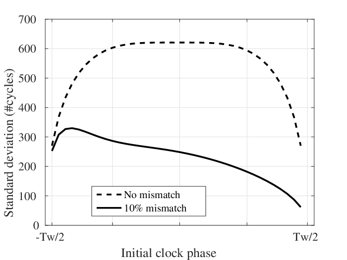
Note that a 10% mismatch in the step size of the left/right shift reduces the mean absorption time by up to 40%. The effect of this mismatch is more pronounced in the standard deviation of the absorption time as a small mismatch is shown to result in a large reduction in the standard deviation as shown in Fig. 38. Hence to reduce the settling time of the circuit, one can deliberately introduce a mismatch in the UP/DN strengths of the charge pump in the circuit. Alternately, a training sequence can also induce a similar mismatch, by producing different amounts of ISI to the two logic levels 0 and 1. This inherently introduces a bias towards one side of the window and reduces the settling time.
VI-B1 Reduction in settling time with charge pump mismatch
Fig. 39 shows the reduction in the settling time of the circuit with the introduction of a 10% mismatch in the UP and the DN currents of the charge pump. Under identical initial conditions, a simulation with 10% mismatch showed 80% reduction in the time taken to exit the window .

Charge pump mismatch, however, can result in increased jitter once the circuit has locked. Simulations of the coarse+fine retiming circuit show that a 10% mismatch in the values of the UP and DN currents increases the peak-to-peak jitter of the recovered clock from 2.04 ps to 2.27 ps, which is approximately a 10% increase in the jitter. This is still only about 0.6% of the clock period of 400 ps which was used in this simulation. If such a performance degradation is not acceptable, the introduced mismatch can be switched off after lock has been achieved.
VI-B2 Reduction in settling time with training sequence
A training sequence that biases the system to either one of the directions can be used to reduce the settling time. For instance, one such training sequence is “…0010011100100111…”. This sequence has a minimum run length of 1 bit for a logic ‘1’ and 2 bits for logic ‘0’. Hence the ISI for logic ‘1’ is always more than that for logic ‘0’ and the phase detector’s output in the window is biased towards the left. For instance, assuming the ISI is limited to 1 previous bit, we can use Table I to compute the probabilities of a corrective action to the left and to the right respectively. In the above bit pattern, we have the following 3 bit sequences: a) “001”, b) “010”, c) “100”, d) “001” e) “011”, f) “111”, g) “110”, h) “100”, which then repeat. Hence, referring to Table I, we see that , and . Hence, this sequence implements a 25% bias to the left.
Fig. 40 shows the control voltage as the circuit settles when (a) the above training sequence “…0010011100100111…” is used, and (b) a random equiprobable binary sequence is used. Notice the considerable reduction in the settling time when the deliberately biased training sequence is used. One could also use an alternating 1 and 0 training sequence which reduces the jitter due to ISI to zero. However, random uncorrelated jitter between the transmitter and receiver clocks may still result in a non-zero size of the window .

VII Conclusions
The effect of jitter on the settling time of mesochronous clock retiming circuits is discussed in detail. In particular, it is shown how ISI induced jitter and random jitter can increase the settling time of clock recovery circuits indefinitely. A model of the system as a Markov chain with absorbing states is developed. Using this model, the effect of different types of jitter is analyzed. The model predictions of the settling time in terms of the mean absorption time of the Markov chain match well with behavioural simulations. Using insights gained from the model, techniques for reducing the settling time are reported. A coarse first synchronizer that uses only coarse correction steps initially is proposed. This architecture achieves small settling times in the presence of substantial ISI. Another technique of reducing the settling time, by introducing a mismatch between the phase updates in either direction of the clock retiming circuit, is also discussed. This is applicable to phase interpolator based clock retiming circuits as well. This mismatch is achieved either by introducing a mismatch in the charge pump or through biased training data. All the suggested fast settling synchronizers are verified with circuit simulations.
Appendices
Appendix A Derivation of the deterministic component of the settling time
For mesochronous systems, a clock running at the correct frequency is available and only the phase has to be corrected. Hence, the clock recovery circuit can be of the first order, i.e., the loop filter is a single capacitor [5, 8]. When a bang-bang phase detector is used, the capacitor voltage () is quantized to a step size given by
Here is the gain of the charge pump, expressed in terms of the charge pump current and the clock period . Hence, the step size of the phase corrections is
| (2) |
The number of phase correction steps () needed for achieving lock can be written as
| (3) |
The settling time can then be written as
| (4) |
where is the data activity factor. From (2), (3) and (4), the settling time expression in (1) follows.
Appendix B Mean time to absorption of a Markov chain
Knowing the probability transition matrix of a Markov chain, the mean time to absorption and its variance can be computed. We will outline an example computation in this Appendix. The state diagram of the Markov chain representation of the clock recovery circuit, for data with 1 bit ISI, is shown in Fig. 17. The states corresponding to and , which are at the edges of the window of susceptibility, are absorbing states. The probability transition matrix for this Markov chain can be written as
To calculate the mean time to absorption (and the variance of the time to absorption), is first written in the canonical form [24]. This is obtained by reordering the entries in to separately aggregate all the transient and absorbing states respectively. Hence, can be written as
Here is a square matrix which captures the transitions from one transient state to another transient state, captures the transitions from transient states to absorbing states and is an identity matrix. The fundamental matrix can be computed using the equation
where is an identity matrix of the same dimensions as . Conditioned on the starting position, the mean time to absorption (), in terms of the number of steps, is given by
where is a column vector with number of rows equal to the number of transient states, and with all entries as 1. The variance of the time to absorption (in terms of number of steps), conditioned on the starting position, is calculated as
Here is obtained by squaring the elements of .
References
- [1] B. Razavi, “Challenges in the design high-speed clock and data recovery circuits,” IEEE Communications Magazine, vol. 40, no. 8, pp. 94–101, 2002.
- [2] J. F. Buckwalter and A. Hajimiri, “Analysis and equalization of data-dependent jitter,” IEEE Journal of Solid-State Circuits, vol. 41, no. 3, pp. 607–620, March 2006.
- [3] N. Kadayinti, A. J. Budkuley, and D. K. Sharma, “Settling time of mesochronous clock re-timing circuits in the presence of timing jitter,” in Proceedings of IEEE International Symposium Circuits and Systems, May 2017, to appear.
- [4] S. H. Lee, S. K. Lee, B. Kim, H. J. Park, and J. Y. Sim, “Current-mode transceiver for silicon interposer channel,” IEEE Journal of Solid-State Circuits, vol. 49, no. 9, pp. 2044–2053, Sept 2014.
- [5] N. Kadayinti, M.S. Baghini, and D.K. Sharma, “A clock retiming circuit for repeaterless low swing on-chip interconnects,” in Proceedings of 30th IEEE Conference on VLSI Design, 2017, pp. 15–20.
- [6] S. H. Chung, Y. J. Kim, Y. H. Kim, and L. S. Kim, “A 10-Gb/s 0.71-pJ/bit forwarded-clock receiver tolerant to high-frequency jitter in 65-nm CMOS,” IEEE Transactions on Circuits and Systems II: Express Briefs, vol. 63, no. 3, pp. 264–268, March 2016.
- [7] M. Hossain and A. Chan Carusone, “7.4 Gb/s 6.8 mW source synchronous receiver in 65 nm CMOS,” IEEE Journal of Solid-State Circuits, vol. 46, no. 6, pp. 1337–1348, June 2011.
- [8] R. Kreienkamp, Ulrich Langmann, C. Zimmermann, T. Aoyama, and H. Siedhoff, “A 10Gb/s CMOS clock and data recovery circuit with an analog phase interpolator,” IEEE Journal of Solid-State Circuits, vol. 40, no. 3, pp. 736–743, March 2005.
- [9] H. Takauchi, Hirotaka Tamura, S. Matsubara, M. Kibune, Y. Doi, T. Chiba, H. Anbutsu, H. Yamaguchi, T. Mori, Motomu Takatsu, K. Gotoh, T. Sakai, and T. Yamamura, “A CMOS multichannel 10Gb/s transceiver,” IEEE Journal of Solid-State Circuits, vol. 38, no. 12, pp. 2094–2100, Dec. 2003.
- [10] B. J. Shastri and D. V. Plant, “5/10-Gb/s burst-mode clock and data recovery based on semiblind oversampling for PONs: Theoretical and experimental,” IEEE Journal of Selected Topics in Quantum Electronics, vol. 16, no. 5, pp. 1298–1320, Sept 2010.
- [11] K. Kishine, H. Inaba, H. Inoue, M. Nakamura, A. Tsuchiya, H. Katsurai, and H. Onodera, “A multi-rate burst-mode CDR using a GVCO with symmetric loops for instantaneous phase locking in 65-nm CMOS,” IEEE Transactions on Circuits and Systems I: Regular Papers, vol. 62, no. 5, pp. 1288–1295, May 2015.
- [12] J. Lee and M. Liu, “A 20-Gb/s burst-mode clock and data recovery circuit using injection-locking technique,” IEEE Journal of Solid-State Circuits, vol. 43, no. 3, pp. 619–630, March 2008.
- [13] M. Hsieh and G. E. Sobelman, “Architectures for multi-gigabit wire-linked clock and data recovery,” IEEE Circuits and Systems Magazine, vol. 8, no. 4, pp. 45–57, Fourth 2008.
- [14] J. W. Joyner, P. Zarkesh-Ha, and J. D. Meindl, “A stochastic global net-length distribution for a three-dimensional system-on-a-chip (3D-SoC),” in Proceedings of the 14th Annual IEEE International ASIC/SOC Conferece, 2001, pp. 147–151.
- [15] P. Zarkesh-Ha, J. A. Davis, and J. D. Meindl, “Prediction of net-length distribution for global interconnects in a heterogeneous system-on-a-chip,” IEEE Transactions on Very Large Scale Integration (VLSI) Systems, vol. 8, no. 6, pp. 649–659, Dec 2000.
- [16] E. Mensink, D. Schinkel, E.A.M. Klumperink, E. van Tuijl, and B. Nauta, “Power efficient gigabit communication over capacitively driven rc-limited on-chip interconnects,” IEEE Journal of Solid-State Circuits, vol. 45, no. 2, pp. 447–457, Feb. 2010.
- [17] B. Kim and V. Stojanovic̀, “An energy-efficient equalized transceiver for RC-dominant channels,” IEEE Journal of Solid-State Circuits, vol. 45, no. 6, pp. 1186–1197, June 2010.
- [18] L. Lamport, “Buridan’s principle,” Foundations of Physics, vol. 42, no. 8, pp. 1056–1066, 2012.
- [19] T. J. Chaney and C. E. Molnar, “Anomalous behavior of synchronizer and arbiter circuits,” IEEE Transactions on Computers, vol. C-22, no. 4, pp. 421–422, April 1973.
- [20] J.D.H. Alexander, “Clock recovery from random binary signals,” Electronics Letters, vol. 11, no. 22, pp. 541–542, October 1975.
- [21] C. R. Hogge, “A self correcting clock recovery circuit,” IEEE Transactions on Electron Devices, vol. 32, no. 12, pp. 2704–2706, Dec 1985.
- [22] Keysight Technologies and TG1B1-A, accessed 2016.
- [23] Keysight Technologies and TG1C1-A, accessed 2016.
- [24] W. Feller, An Introduction to Probability Theory and Its Applications, vol. 1, Wiley Sons and Inc., January 1968.
- [25] P. K. Hanumolu, G. Y. Wei, and U. K. Moon, “A wide-tracking range clock and data recovery circuit,” IEEE Journal of Solid-State Circuits, vol. 43, no. 2, pp. 425–439, Feb 2008.
- [26] H. Song, D. S. Kim, D. H. Oh, S. Kim, and D. K. Jeong, “A 1.0-4.0-Gb/s all-digital CDR with 1.0-ps period resolution DCO and adaptive proportional gain control,” IEEE Journal of Solid-State Circuits, vol. 46, no. 2, pp. 424–434, Feb 2011.
- [27] J. Buckwalter, B. Analui, and A. Hajimiri, “Predicting data-dependent jitter,” IEEE Transactions on Circuits and Systems II: Express Briefs, vol. 51, no. 9, pp. 453–457, Sept 2004.
- [28] A. Demir, A. Mehrotra, and J. Roychowdhury, “Phase noise in oscillators: a unifying theory and numerical methods for characterization,” IEEE Transactions on Circuits and Systems I: Fundamental Theory and Applications, vol. 47, no. 5, pp. 655–674, May 2000.
- [29] L. Ravezzi and H. Partovi, “Clock and synchronization networks for a 3 GHz 64 bit ARMv8 8-Core SoC,” IEEE Journal of Solid-State Circuits, vol. 50, no. 7, pp. 1702–1710, July 2015.
- [30] N. Kadayinti and D. K. Sharma, “Testable design of repeaterless low swing on-chip interconnect,” in Proceedings of Design, Automation and Test in Europe (DATE), March 2016, pp. 563–566.
![[Uncaptioned image]](1604.00230v3/naveen.png) |
Naveen Kadayinti received his M.Tech + Ph.D. dual degree from the Indian Institute of Technology Bombay in 2017. He is currently an Assistant Professor in the Department of Electrical Engineering at the Indian Institute of Technology Dharwad. He was a visiting faculty member in the Department of Avionics at the Indian Institute of Space Science and Technology Trivandrum during Spring 2017-18. His research interests include wired and wireless communication circuits and mixed signal SoC design and test. |
![[Uncaptioned image]](1604.00230v3/amitalok.png) |
Amitalok J. Budkuley received the B.E. degree in Electronics and Telecommunications Engineering from Goa University, Goa, India in 2007, and the M.Tech. and Ph.D. degree in Electrical Engineering from the Indian Institute of Technology Bombay, Mumbai, India in 2009 and 2017 respectively. From 2009 to 2010, he was with Cisco Systems, Bangalore, India. He is currently a Postdoctoral Researcher at the Department of Information Engineering, The Chinese University of Hong Kong, Sha Tin, Hong Kong. His research interests include information theory, communication systems and game theory. |
![[Uncaptioned image]](1604.00230v3/Maryam.png) |
Maryam Shojaei Baghini (M’00 - SM’09) received the M.S. and Ph.D. degrees in electrical engineering from Sharif University of Technology, Tehran, in 1991 and 1999, respectively. She has worked for more than 2 years in industry on the design of analog ICs. In 2001, she joined Department of Electrical Engineering, IIT-Bombay, as a Postdoctoral Fellow, where she is currently a Professor. She is the author/coauthor of 143 international journal and conference papers, the inventor/coinventor of 6 granted US patents, 1 granted Indian patent and 25 more filed patent applications. Her current research interests include high-speed links for on-chip and off-chip data communication, high-performance low-energy analog/mixed-signal/RF IC design and test for various applications including healthcare and sensor networks, device-circuit co-design in emerging technologies and energy harvesting circuits and systems. Dr. Shojaei serves in the Technical Program Committee of several IEEE conferences, including IEEE International Conference on VLSI Design, and Asia Symposium on Quality Electronic Design. She was a TPC member of IEEE-ASSC from 2009 to 2014. Dr. Shojaei is joint recipient of 11 awards and a senior member of IEEE. |
![[Uncaptioned image]](1604.00230v3/dinesh.png) |
Dinesh Sharma obtained his Ph.D. from the Tata Institute of Fundamental Research, Mumbai. He has worked at TIFR and IITB at Mumbai, at LETI at Grenoble in France and at the Microelectronics Center of North Carolina in the U.S.A. on MOS technology, devices and mixed mode circuit design. He has been at the EE deptt. of IIT Bombay since 1991, where he is currently a Professor. His current interests include mixed signal design, interconnect technology and the impact of technology on design styles. He is a senior member of IEEE, a fellow of IETE and has served on the editorial board of ”Pramana”, published by the Indian Academy of Science. |