Ion-beam nanopatterning of silicon surfaces under co-deposition of non-silicide-forming impurities
Abstract
We report experiments on surface nanopatterning of Si targets which are irradiated with 2 keV Ar+ ions impinging at near-glancing incidence, under concurrent co-deposition of Au impurities simultaneously extracted from a gold target by the same ion beam. Previous recent experiments by a number of groups suggest that silicide formation is a prerequisite for pattern formation in the presence of metallic impurities. In spite of the fact that Au is known not to form stable compounds with the Si atoms, ripples nonetheless emerge in our experiments with nanometric wavelengths and small amplitudes, and with an orientation that changes with distance to the Au source. We provide results of sample analysis through Auger electron and energy-dispersive X-ray spectroscopies for their space-resolved chemical composition, and through atomic force, scanning transmission electron, and high-resolution transmission microscopies for their morphological properties. We discuss these findings in the light of current continuum models for this class of systems. The composition of and the dynamics within the near-surface amorphized layer that ensues is expected to play a relevant role to account for the unexpected formation of these surface structures.
pacs
79.20.Rf, 81.16.Rf, 68.35.Ct, 05.45.-aI Introduction
Ion beam irradiation employing low energy noble gas ions is a functional tool to obtain nanoscale surface patterns in a diversity of materials. [1] Under proper conditions these patterns can be ordered over large lateral distances in comparison to their heights.[2] In particular, and due to their technological relevance, much work has been focused on the formation of such surface nanostructures on silicon.[3] The first experiment reporting the formation of silicon nanopatterns by ion irradiation was published in Ref. 4, in which 1.2 keV Ar+ ions were employed to form ordered nanodots on a Si substrate. Despite many experiments having shown the formation of a large variety of nanostructures on silicon surfaces, it turned out that most of these results were due to the effect of impurities incorporation.[3] This is, at least, the case for small angles of incidence as first noted by Ozaydin et al.[5] In this work, the authors brought to light the importance of a continuous metal supply to enhance the pattern formation. Thus, only silicon substrates with metal impurity concentrations above a certain threshold may develop nanostructures at normal incidence.[6] This point was confirmed by Madi et al., who showed the absence of surface nanopatterns for Ar+ ions at different energies and clean conditions, for incidence angles smaller than 48∘.[7] Above this angle, and up to 80∘, the formation of perpendicular ripples was reported, with wavevector parallel to the projection of the ion beam.
Recent efforts have explored the morphologies formed under systematic impurity incorporation in order to better understand this process and the intervening physical mechanisms. In this line, in 2008 Hofsäss and Zhang proposed a setup combining ion irradiation and atom deposition to study ripple formation on silicon surfaces at 70∘ and 80∘ with 5 keV Xe+ ions.[8] This technique, known as surfactant sputtering, consists on locating an adjacent plate with a certain tilt next to the substrate. This experimental geometry allows to modify substrate composition and irradiation conditions, since the plate is co-sputtered during ion bombardment and some material is deposited on the substrate. In this experiment, ripples properties were altered depending on the plate material and the distance to it. For instance, the substrate surface roughness was found to increase with the distance to a gold plate. In contrast to the previous experiment in which ripples are formed for large angles of incidence in the absence of contamination, in Refs. 9 and 10 similar setups were employed with smaller angles of incidence and an iron plate perpendicular to the substrate, and allowing for different angular locations, respectively. In these experiments, due to redeposition, metal content is maximum next to the plate location and decreases with the distance to it. The sputtered metallic material (and perhaps reflected ions) influences pattern appearance, which would not be formed without this surfactant sputtering. Using 2 keV Kr+ ions at 30∘, in Ref. 9 different pattern types were observed depending on the distance to the plate. Similarly, parallel mode ripples and dots far from the plate were observed in Ref. 10 using 5 keV Xe+ ions at normal incidence. Later works have confirmed the dependence of the topography on the plate distance at low temperatures, ,[11] confirming metal silicide formation and its segregation as key mechanisms to induce pattern formation. Silicide-induced patterning was also recently studied by surfactant sputtering employing different co-deposited materials in Refs. 12 and 13, in which the requisite of silicide formation to observe silicon nanopatterning was confirmed for 5 keV Xe+ ions at 60∘ and 2 keV Kr+ ions at 30∘, respectively. Interestingly, in the former work, no ripple formation was observed for the case of copper and gold contamination, suggesting that only materials leading to silicide phase separation may form patterns on silicon substrates.
Although the mechanisms inducing pattern formation under surfactant sputtering are not yet completely understood, from the previous experimental results it seems convenient to distinguish between two different cases: when selective formation of silicide occurs, and when silicon and impurities do not react chemically. The former case has been addressed theoretically in Ref 14, where a mathematical model is formulated to describe the height and composition evolutions for normal incidence bombardment and oblique deposition. It is found that silicide formation and the interaction between the surface composition and morphology are crucial to destabilize the surface. For the case in which silicon and impurities do not react chemically, some theoretical works predict pattern formation when impurity deposition is simultaneous to ion bombardment.[15, 16, 17, 18] These models predict, for instance, a pattern instability that can emerge purely as the result of the difference in the sputtering yields for both species[18] when a minimal impurity concentration value is reached.[16] A more extended revision of these models will be provided in Section IV.
In order to check the possibility of nanopattern production for the case of non-silicide formation, in this paper we have conducted experiments in which Au atoms were co-deposited over a silicon substrate using the surfactant sputtering technique. It is important to stress that gold does not form stable silicide, but a metastable alloy with Si within a wide range of compositions below its eutectic temperature.[12] In the experiment described below, well-defined nanopatterns with different features were found on the Si substrate, indicating that silicide formation is not a necessary condition for pattern formation. Based on our experimental findings, we will try to rationalize the role of Au impurities and how the formation of Si nanopatterns is catalyzed by them.
The paper is organized as follows. Section II is devoted to describe our experimental setup, while results thus obtained are reported in detail in Sec. III. A rationalization of our observations in the light of current continuum descriptions of the process is contained in Sec. IV. This is followed by a discussion in Sec. V. The paper closes by summarizing our main results and conclusions in Sec. VI.
II Experiments
Ion-beam sputtering (IBS) has been performed in a custom-built ultrahigh vacuum chamber with a base pressure of mid-10-10 Torr. We have used an (99.999 %) Ar gas as the ion source. The ion energy was 2 keV, and the ion flux was 1.59 ions nm-2s-1, which is estimated from the target current. Since secondary electrons are not taken into account, this is only a nominal value for which sets an upper limit for the actual ion flux. All the images are taken for fixed fluence of 8,586 ions nm-2. We have used a Kauffman-type ion gun (IQE-11, SPECS), the beam diameter being mm.
Before loading the sample into the chamber for IBS, 10 mm 10 mm Si(100) chips were immersed into a HF solution (99% H2O + 1% HF) for 5 seconds, in order to remove the natural oxide from the surface, and then rinsed by de-ionized water. For the co-deposition of Au during IBS, we mounted the Si sample at the edge of a single crystalline (99.999%, Mateck) Au(001) target at a right angle, using a silicon glue. Thus, the ion-beam simultaneously irradiated both the Si(100) at a near-glancing angle of 75∘ and the Au sample at 15∘ from the respective surface normals, see Fig. 1.
In order to align the ion beam, we placed two 100 nm-thick Au films deposited on Si(100) in the same experimental geometry as shown in Fig. 1, and irradiated the films with the Ar+ ion beam as specified above. The location and the profile of the beam on the target surfaces is, then, identified by the erosion profile of the Au films. That information is used to adjust the beam to be well inside the sample, precluding impurity deposition from the sample holder, as also confirmed by Auger electron spectroscopy (AES).
After sputtering the sample, its surface topography was investigated ex situ by both an atomic force microscope (AFM, XE-100, Park Systems) in the tapping mode and a scanning electron microscope (SEM, JSM-7600F, JEOL). The cross-sectional specimen for the transmission electron microscope (TEM) analysis was prepared using a conventional ion-mill procedure after mechanically grinding the specimen. TEM (JEM 2100F, JEOL) was operated at an acceleration voltage of 200 kV for both the high-resolution (HR-TEM) and scanning transmission electron microscopy (STEM) modes. An annular dark field (ADF) detector ranging from 100 to 250 mrad was used for high angle annular dark field (HAADF) imaging. Energy dispersive X-ray spectroscopy (EDX) analysis was carried out simultaneously with the HAADF-STEM imaging. Depth profiling was also performed by taking Auger electron spectra (PHI Nanoprobe 700), while raster-sputtering a 3 mm3 mm area with the Ar+ beam.
III Results
Figure 2 shows typical (a) 3 m2 and (b) 1 m2 Si surfaces after IBS under the stated sputtering condition, in the absence of gold codeposition.
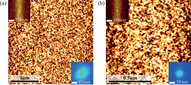
No surface pattern is detectable, as suggested by the auto-correlation function and 2D Fourier transform (FT) provided in the top left and bottom right insets of each image, respectively. For a height profile , the auto-correlation function is defined as , where denotes a point on the target plane and the brackets denote average with respect to the position of the reference point . For the sputtered surfaces in Fig. 2, the values of the surface roughness or width, , are (a) 0.2 nm and (b) 0.1 nm, respectively. These values are similar to those of the Si substrate prior to irradiation. Here, is defined by , where is the mean height at time . The bracket denotes the average over the imaged space.
Figure 3 presents the surface topographies obtained at four different sites on the Si(100) target after IBS with concurrent Au co-deposition. In sharp contrast to the case of clean Si(100), now well-defined nanopatterns form. Note that the pattern changes from (a) to (d) in Fig. 3 as the imaging site is further away from the Au source and the flux of co-deposited Au impurities becomes smaller.
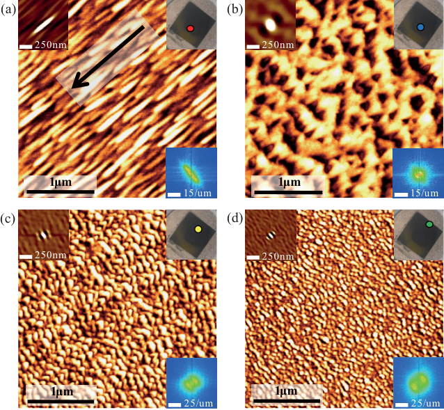
Figure 3(a) shows a ripple pattern near the Au source (site 1), as indicated in the upper-right inset. As seen in the real-space image and consistent with the 2D autocorrelation and FT provided in the insets, the ridges of the ripples run along the projection of the ion beam direction, their wavelength being close to 120 nm. This is the same ripple orientation as obtained on pure Au(001) targets under a similar sputtering condition.[19] The mean uninterrupted ridge length of the ripples (m), or coherence length, is, nevertheless, much shorter than that for Au(001). Ripple growth in this relatively Au-rich region is probably interrupted by chemical and structural defects, such as segregated Au nano-clusters, as observed in the TEM images shown later.
Figure 4(a) shows the 1D power spectral densities (PSD) along the two different directions on the substrate plane, namely, the squared modulus of the FT of 1D cuts of the surface in Fig. 3(a) along each direction. From now on, corresponds to the projection of the ion beam and is the perpendicular direction. In the figure one can clearly identify a characteristic wave-vector value along the -axis, m-1, at which an abrupt change takes place in the slope of the curve. This value corresponds to the mean wavelength mode of the observed ripple pattern. In contrast, there is no such feature along the -axis, parallel to the ion beam direction. Since the ripples ridges are thus parallel to the latter, we term these parallel ripples.
Figure 3(b) shows the pattern observed 0.75 mm away from site 1 and the Au source (site 2), as indicated in the inset at the upper-right corner. As suggested by the 2D autocorrelation and FT, patterning seems to be occurring along the two substrate directions. Along the ion beam direction, ripples still develop, with very short coherence lengths. Perpendicular to the ion beam direction, shortened ripples concatenate with neighboring ones to form an array of stripes. The two 1D PSD curves along the and directions almost coincide for this pattern, see Fig. 4(b), reflecting the two-dimensional nature of the structure. Along the -direction, though, one can observe a broad peak, reflecting a prominent ripple-like texture with a wave-vector running along the ion beam direction. Such a quasi-two-dimensional pattern is often observed during ripple reorientation transitions.[20] In our system, the transition properly takes place when one moves further away from the Au source as detailed below. From now on, the region represented by the site 2 is thus termed transition region.
Figure 3(c) shows an image taken further away from the Au source, at site 3. A well-defined ripple pattern is observed, but now the ripple ridges run perpendicular to the ion beam direction, so that ripple re-orientation has fully taken place. We term these perpendicular ripples. Accordingly, in Fig. 4(c) the PSD along the -direction clearly shows a sharp peak at a well-defined mean wavelength, characteristic of the perpendicular ripple pattern. Considering that, under the same sputtering condition, IBS produces parallel ripples both for bulk[19] Au(001) and for the relatively Au-rich region in Fig. 3(a), the perpendicular ripple in Fig. 3(c) and the reorientation transition seem triggered by the reduced Au concentration, sufficiently far away from the Au impurity source.

Finally, Fig. 3(d) shows an image at the farthest position from the Au source, site 4. One can still observe a perpendicular ripple pattern, the corresponding PSDs clearly showing a well-defined peak along the -direction [Fig. 4(d)], which corresponds to the mean wavelength of these perpendicular ripples. The mean wavelength and surface roughness of these ripples are smaller than those at site 3, as summarized in Fig. 5(b). Moving away from the Au source, and thus for a reduced Au flux, the surface at site 4 behaves more like clean Si(100), which shows very efficient healing kinetics leading to virtually flat surfaces under the present sputtering condition, as shown in Fig. 2.
The perpendicular ripples in both Figs. 3(c) and (d) are, however, wiggly; each ridge looks either sectioned into small pieces or with a very small coherence length. This suggests that the instability along the direction perpendicular to the ripples still remains effective enough, so as to induce sectioning of the ripple ridges. Moreover, each piece has neither a uniform width nor a sinusoidal shape, pointing to the significance of non-linear effects.[21, 3]
Previous experimental[8, 9, 11, 10, 22, 23, 13] and theoretical [18, 14] results indicate that the direction of the wave-vector of the ripple pattern follows that of the impurity flux. Although these experimental results are obtained for silicide-forming metallic impurities, which is not the case in our system, the perpendicular ripple patterns we observe at the sites 3 and 4 indeed seem consistent with such results. Figure 5(a) depicts the sputtering geometry and also the recoil geometry in real scale, including sketches of the directions of the Au impurity flux reaching the four sites. In the previous experiments,[8, 9, 11, 10, 22, 23, 13] the incidence of the ion beam is near normal to the average surface orientation, or its influence is isotropic. In our case, however, the ion beam incidence is close to glancing.
In the relatively Au-rich region, the target behaves as a pure Au surface in the erosive regime,[19] for which recrystallization is very efficient,[24] irradiation-induced material rearrangement or viscous flow is negligible,[3] and the morphological instability seems to be of the erosive Bradley-Harper[25] (BH) type.[26] This accounts for the parallel ripple orientation. In the opposite limit in which Au impurities are scarce, purely erosive mechanisms are less effective in the Si-like surface (recall no pattern forms in the absence of impurities), surface material rearrangement or viscous flow being expected to be more relevant.[3] Still, the direction of the Au flux may be influencing the orientation of the ripple pattern, as frequently observed in other experiments. The 2D-like pattern in between the two, relatively Au-rich and Au-poor, regions [Fig. 3(b)] may result from the balance of the two driving forces. We have performed SRIM simulations[27] (not shown) and obtained that the sputtering yield of the recoiled Au impurities is negligible. However, the recoiled Au atoms do transfer their momentum to the Si atoms and can displace them by close to 1 nm. This mass displacement might drive the ripple orientation inducing Carter-Vishnyakov-like (CV) surface-rearrangement currents.[28] Recall that, for high-incidence angles, CV effects actually destabilize the surface and contribute to ripple formation.
Figure 6 shows depth profiles of our samples showing the atomic weight percent of Au and Si obtained by AES.

The measurement is made at three different locations: At the vicinity of the Au source, in between sites 1 and 2, and close to site 3, as shown in the inset of Fig. 6. Since the depth profile is taken over a 3 mm3 mm, raster-sputtered area, the spatial resolution is limited by the same scale. From the profiles, we can clearly see that, as expected, the Au content is higher for locations which are closer to the Au source. The nominal atomic weight percentages of Au at the surface decrease from 100% to 30% (5.8% of the atomic concentration), and then to 18% (3.0% of the atomic concentration) as moving further away from the Au source. The values are nominal, since they are calculated by assuming that the concentration of Au is vertically uniform, or at least within the escape depth of the Au AES electrons. The residual Au impurities are confined within a layer which is approximately 5 nm deep, except for the Au-like film formed closest to the Au target. This thickness is comparable to that of the amorphized topmost surface layer that is revealed by HRTEM and STEM (Figs. 7 and 8). Note that the amplitude of the nanostructures formed by IBS is less than 2 nm [cf. Fig. 5(b)]. Thus, the nanostructures form solely in the Au containing region, indicative of the active role of the Au impurities in the pattern formation.


Fig. 7(a), the HRTEM image around site 1, shows that the surface region is made of an amorphous Si layer embracing Au nanoclusters. The yellow dotted circles indicate crystalline clusters displaying regularly spaced lines oriented differently in different regions, but having distinctly different spacing from that of crystalline Si. These clusters seem to be formed of the co-deposited, but segregated, Au impurities, due to the high Au concentration in this region. On the other hand, their surroundings show no ordered features, and are reminiscent of an amorphous region formed of Si possibly with very disperse Au impurities. For regions which are further away from the Au source [panels (b) through (d) in Fig. 7], no Au nanoclusters in the amorphized layer can be detected by HRTEM, the layer structure looking more homogeneous from this point of view.
We have further characterized the chemical structure of our samples through the EDX in conjunction with High-angle annular dark-field scanning transmission electron microscope (HAADF-STEM). The HAADF-STEM image in Fig. 8(a) shows the interface with clear contrast in its intensity. Fig. 8(a’) shows the Au EDX signal along a line normal to the interface in the boxed region in Fig. 8(a). It clealy tells that the high intensity in Fig. 8(a) originates from the high Au concentration. Since Au does not form stable silicides,[23] we should expect phase separation in the form of Au clusters. Metastable clusters of Au silicide have been reported only at elevated temperatures.[29]
Within the alloyed layer in Fig. 8(a), the Au impurity concentration looks higher around the ridge than around valleys. High impurity concentration around ridges is commonly observed for many silicide-forming impurities.[8, 9, 11, 10, 22, 23, 13] In those systems, phase separation associated with silicide formation is thought to be at the origin of the surface nanopatterning. In principle, it is thus tempting to conclude that phase separation of Au, and an inhomogeneous sputtering yield distribution, also induces the observed pattern formation in our case.
However, note that SRIM calculations[27] under our present condition lead to virtually identical sputtering yields for Au and Si, see Fig. 9.

Hence, apparently phase separation does not lead to an inhomogeneous sputtering yield over the surface, and thus to pattern formation. Still, as recently pointed out,[13] rapid segregation of Au under a constant external deposition flux makes the apparent sputtering yield of phase-separated Au much smaller than that of Si, since the external Au supply constantly replenishes the sputtered Au. This effectively-lower Au sputtering yield, then, might in turn lead to pattern formation. Within this scenario, surface valleys erode faster due to the relatively low-Au concentrations, as compared with the ridge region.
Further away from the Au source, the Au flux is low and the alloyed layer is thin as shown in Fig. 8(b) and (c) consistently with the narrowed, (dark) Au containing layers in Fig. 7(c) and (d), respectively. They do not reveal clear modulation of the Au concentration in the substrate plane. Thus, at this moment we may not be able to contend that the patterns observed in the relatively Au-poor region have the same origin as in the Au-rich region. Note, our failure to observe a compositional pattern in the impurity-poor regions may be due to the low Au concentration there. Combined with a low spatial resolution of HAADF-STEM image, this result may hamper detection of small modulations of the impurity concentration, even if they actually exist.
IV Comparison with continuum models
To date, a number of continuum models are available in the literature (some of which have been already mentioned), in which surface nanopattern formation is described in the presence of non-negligible impurity co-deposition, see an overview in Ref. 3. For instance, an early work for so-called surfactant sputtering [30] put forward a coupled system of equations [31, 32] for the dynamics of the surface height and the surfactant concentration, although no predictions were provided for dependencies of the pattern properties with experimental parameters. More recently, related approaches have been pursued in greater detail, considering the effects of various incidence conditions and relaxation mechanisms. Thus, concurrent impingement of ions and impurities has been considered, [15, 16, 17] leading to e.g. an analytical result [16] on a minimal threshold value which is required for the impurity concentration so that patterns can appear. A generalization to oblique ion and impurity incidences has then been performed,[18] with the result that an instability can arise purely as a result of differential sputtering rates for the two impinging species, in interplay with a phase shift between the concentration and the height profiles. More recently,[14] silicide formation has been explicitly incorporated to the models, with the conclusion that it plays a decisive role, in agreement with many experimental results as already discussed.
In this section we put the results of the experiments described in Sections II and III in the light of these continuum models, with the aim to stress similarities and differences between predictions and observations. Although such a discussion will allow to somewhat rationalize the latter, it will mostly suggest issues that should possibly be taken into account for model improvement, to be able to account for the experimental results.
Two very basic experimental observations can be taken as a first basis for modeling: (i) Under the chosen irradiation conditions, pure Si targets are morphologically stable, while Au targets are not. (ii) There is a space gradient in the Au impurity concentration within the Si target: this concentration is maximum near the Au source and it decreases with distance to the latter. Moreover, we can add the result from our SRIM simulations shown in Fig. 9 that, (iii) at the ion energy and incidence angle considered, the sputtering yields of Au and Si take the same values.
These observations can be readily implemented in the phenomenological model originally put forward in Ref. 16 for ion-beam sputtering of a monoelemental target of atomic species (silicon in our experiment), under simultaneous co-deposition of impurities of a different species (gold, in our case). Further important assumptions which agree with our experimental results include that the two atomic species are mutually inert, i.e. they form no compound; and that a surface layer, of thickness , forms on top of the irradiated target, within which there is deposition of species , both species being subject to transport and sputtering effects. We should note that in this model [16] ions and impurities arrive under normal incidence, in stark difference with the present experiments. However, for the sake of simplicity we first proceed by neglecting this fact. Likewise, we restrict ourselves to a one-dimensional system. We will come back to these assumptions later.
The model consists of the following two coupled equations:[16]
| (1) | |||||
| (2) |
Here, is the deposition flux of impurities, their space-time-dependent surface concentration (such that ), is the atomic volume of both species, assumed to be equal for simplicity, is the height of the irradiated target, and and are, respectively, the erosion flux and surface current of species . More specifically,
| (3) |
where is a constant and is the sputtering yield of the species, such that for erosion is more efficient at surface troughs than at surface peaks, as in the classic Bradley-Harper (BH) mechanism.[25] Finally, the surface current is
| (4) |
where the first term on the rhs is Fickian diffusion ( is surface diffusivity and the areal density of mobile surface atoms), the second one is Mullins’ surface diffusion ( is surface tension and is temperature), and the last one is a stabilizing Carter-Vishnyakov (CV) term,[28] in which . For our experimental system, for which the topmost surface layer can be thought of as an amorphous Si phase with Au impurities, CV terms can be thought of as proxies of surface-confined viscous flow, recently shown to describe IBS patterning of clean Si targets.[33, 34, 32, 35, 36, 37, 38, 39, 40] In such a case, the coefficient in front of the third order derivative term in should more properly be related with radiation-induced viscosity. Nevertheless, this fact does not play a relevant role in the discussion to follow. Similarly, note that pure Au targets recrystallize very efficiently under our experimental conditions, so that is small as discussed above, at least in regions where the Au density is high enough that recrystallization becomes feasible.
The analysis of model (1)-(4) performed in Ref. 16 corresponds to the case of immobile impurities, i.e., . Moreover, a coordinate rescaling is performed [16, 17] by constants which are inversely proportional to the sputtering yield difference, . But, because of the SRIM result from Fig. 9, we are interested in a system with the same sputtering yields for both species, for which this parameter combination is zero.
We have performed a linear stability analysis of the full model (1)-(4) for precisely the case in which and . The result is that the model supports a flat solution and , characterized by a constant surface velocity and uniform impurity coverage . Moreover, under the standard large-wavelength approximation (namely, for wave-vectors ), the linear dispersion relation for periodic perturbations of this flat solution, and , where ,[16] reads
| (5) |
Naturally, both and depend on the parameters entering model (1)-(4). For our case of interest, we obtain
| (6) |
and
| (7) |
where .
The morphological stability of the surface is controlled by the sign of the constant in Eq. (6), in a way that in principle agrees with the simplest expectations: If the impurity concentration is very large (), then because gold is under a pattern-forming condition (CV effects, , are negligible with respect to BH effects, ), thus the system displays pattern formation. Conversely, for very low impurity concentration (), then , which rules out unstable modes and pattern formation, because Si is under such stable conditions (CV contributions, , dominate over BH effects, ). Actually, there is a threshold impurity concentration, , such that patterns form only provided .
Thus, model (1)-(4) can in principle rationalize the basic experimental fact that Au impurities lead to pattern formation in our Si targets. However, a number of further considerations have to be made at this point:
- •
Although in the experimental system the reference surface concentration of impurities is not a space-independent constant as assumed in the model, the variation of the deposition flux across the experimental system does occur in macroscopic scales which are much larger than the ripple wavelength. On the other hand, in our experiments we obtain ripple formation throughout the sample, while the model leads to expecting flat surfaces for regions where . This was checked in Fig. 2, but perhaps we did not employ large enough targets, with areas sufficiently far from the Au source, featuring no surface pattern.
- •
Whenever pattern formation occurs in the model topography, a space modulation simultaneously takes place in the composition field. As discussed in Sec. III, in the experiments such type of composition pattern is seen in the relatively Au-rich regions only, being possibly beyond detection limit in the Au-poorer regions, for the experimental technique employed.
- •
The model suggests that, in regions where the impurity concentration takes intermediate values, ripple formation is analogous to what is seen for a pure Au system. However, this is not the case in the experiments either: in the former case perpendicular ripples are observed, while parallel ripples form on the relatively Au-rich regions which are very close to the impurity source.
The lack of simultaneous patterning in the surface morphology and composition suggests the need for a closer experimental characterization of the space distribution of atomic species in the amorphized surface layer that ensues. From the general point of view of reaction-diffusion type models,[41] like the present two-field model (1)-(4),[3] simultaneous patterning of the two fields, i.e., height and impurity concentration, is the rule rather than the exception.
On the other hand, indeed the assumption of normal incidence for both, ions and impurity atoms recoiling from the gold source, is an overly simplifying one. On the basis of the mentioned IBS experiments on Si targets with concurrent silicide-forming impurity co-deposition, a high relative angle between the ions and impurities has been suggested to facilitate pattern formation.[13] Moreover, the results in Sect. III show a rotation of the ripple structure with increasing Au concentration. Thus, a two-dimensional generalization of model (1)-(4) is required, for arbitrary ion and impurity incidence angles. This will lead in particular to an anisotropic version of the linear dispersion relation (5)-(7). However, it is not obvious that this can improve the results on the ripple orientation as a function of impurity concentration . This is because, experimentally, the axis is the only unstable direction for Au, while both directions are stable for Si. Therefore, a convex linear combination of the (2D anisotropic generalizations of the) Au and Si 2D linear dispersion relations, such as Eq. (6) is, cannot possibly yield an unstable direction, as would be needed to explain the ripple orientation for intermediate impurity concentrations.
In the search for alternative models to account for the present observations, we note that, although formulated for (impurity-free) IBS of binary systems, a model has been put forward [42] in which (ion-assisted) phase-separation can control the nano structuring process. In this work it is concluded that pattern formation will occur only if phase separation in the amorphized layer is fast enough so that it completes before the layer is sputtered away. Moreover, the morphological transition in such a case leads to highly ordered patterns. The large degree of disorder in the perpendicular ripple structures we observe, and the relative homogeneity of the amorphous layer in the corresponding regions, both contrast with these theoretical results.
Seeking for further theoretical descriptions, recall that, for pure Si targets, ripple formation has been recently accounted for on the basis of viscous flow of the topmost amorphized layer.[34, 32, 35, 36, 37, 38, 39, 40]In this approach, a crucial effect of ion irradiation is inducing residual stress in the amorphous layer, which is relaxed via solid flow. The characteristics of the surface dynamics are contingent upon the properties of the non-homogeneous stress distribution that builds up within the layer,[38, 39] which in particular controls the value of the critical incidence angle for the ions, above which perpendicular ripples form. In our present experiment, ripple formation does not occur on uncontaminated Si, namely , which we expect to originate in the properties of the stress distribution under the corresponding conditions. Recently, a similar result has been accounted for [43] on the basis of material redistribution using a Monte Carlo-based crater function approach, which we believe can constitute an equivalent, microscopic-based description of viscous flow. Under this scenario, perpendicular ripple formation in our experiments for intermediate impurity concentration might occur due to the influence of Au impurities in the stress distribution. Indeed, recall the results of our SRIM simulations that recoiled Au atoms transfer momentum to the Si atoms and can displace them by close to 1 nm. Such a displacement may reflect into a modified stress distribution, to such an extent that it may be responsible for the formation of perpendicular ripples. In the relatively Au-rich regions, due to efficient recrystallization, the high gold coverage would override viscous flow and lead to parallel ripple formation, akin to a pure Au target under the same sputtering conditions.
V Discussion
Our experimental results show that, under conditions for which pure Si targets do not become structured under IBS, Au impurities can induce surface pattern formation, in a way that is correlated with the impurity concentration. This is in spite of the fact that, as discussed in detail elsewhere,[23] no silicide is expected to form for our combination or materials. Already at the low Au concentration values reached far ( mm) from the impurity source, a perpendicular ripple pattern forms, which is strongly disordered and has small wavelength and amplitude. The orientation of these ripples conforms to expectations based on silicide-forming impurities,[13] that a large relative angle between ions and recoiling impurity atoms, , enhances pattern formation. In our case, such an angle value is large indeed, . This fact may account for the disagreement between some of our experimental observations and currently available models, usually studied for small .
Closer to the gold plate, for moderate but increasing impurity concentration values, the wavelength of the perpendicular ripples also increases. However, in this range of Au concentration values we have not been able to detect a direct correlation between the behaviors of the topography and the composition, i.e., we do not find a space modulation of Au concentration field. If there is any, it remains beyond detection limit for the STEM measurements reported in Sec. III. This fact calls for a more detailed experimental assessment of the impurity concentration, with respect to both, the substrate coordinates (composition modulation) and the depth along the thickness of the amorphized layer.
Actually, co-deposition of Au impurities has been already attempted previously[23, 13] in order to surface pattern Si through IBS, to no effect. The experimental conditions employed in these works are nevertheless different from ours, the most notable difference is our large relative angle between ions and the recoiling Au atoms. Engler et al. already [13] suggested experimental setups with large to maximize the coupling between height fluctuations and the concentration modulation via shadowing effects. A second major feature of our setup is the large ion incidence angle, , employed. In our case . This also stems from an observation by Engler et al. They observed that large incidence angles drive Si marginally stable, already without Au co-deposition. These might have also triggered our system into the unstable state, giving the patterns we observe. As a third difference with previous works, we have used Ar+ ions, which are lighter than previous choices, such as Xe+ or Kr+. Note that the use of light elements as projectiles does not necessarily enhance pattern formation in the absence of impurity co-deposition. Thus, under our sputtering condition Ar+ does not induce ripple formation on clean Si, while Kr+ does.[13] Indeed, the ion/target mass ratio is known to play a non-trivial role in the ion-induced stress distribution and thus in the patterning properties of Si.[38, 40] Increased momentum transfer from the use of heavy projectiles is supposed to drive the Si substrate into the unstable state. In short, our experimental combination of relatively high and values seems to cooperatively destabilize the Si surface under IBS for relatively low impurity concentrations. Then, the space modulation of the latter, coupled to height fluctuations, might have led to the observed perpendicular ripple patterns. This picture needs to be taken with caution, since precisely in the Au-poor regions we cannot detect the modulation of the Au concentration profile.
For locations which are sufficiently close to the Au source, impurities are able to form clusters, as seen in our HR TEM images, which appear to be dispersed within an amorphous Si matrix. Morphologically, this seems sufficient for the surface to display parallel ripples, very much akin to those obtained on pure Au films. The concentration of Au which is required for this behavior has a moderate value near . Close to it, the morphological behavior corresponds to a transition between the topographies observed for relatively low and relatively high Au concentrations. Thus, somehow a superposition of the two ripple structures is observed, characterized (recall the PSD curves in Fig. 4) by an increase of the ripple wavelength in the direction until disappearance of the characteristic scale along this direction for increasing Au concentration. This occurs together with simultaneous appearance of a characteristic wavelength along the direction. The behavior of the PSD curves seems reminiscent[41] of a morphological Type II transition along the direction and a Type I transition along the direction: indeed,[41] in a Type II transition the characteristic wavelength diverges when approaching the transition point from the pattern-forming side. This is actually the experimentally observed behavior for pure sapphire[44] or Si targets in the absence of impurities at low energies.[45, 46, 7, 47, 36, 38] In contrast, a Type I morphological transition features the sudden appearance of a characteristic wavelength at the corresponding transition point.[41] To date, there seem to be no experimental observations of Type I transitions in the context of IBS surface nanopatterning.[47] Note an alternative scenario is actually feasible for our experimental results, as already discussed above: The coherence length along the axis of the low-Au-concentration ripples may be indicating that the corresponding wave-vector corresponds to an unstable Fourier mode of the height, which is not the most dominant mode for such Au concentration values, but becomes so at a sufficiently high value of the impurity concentration. Hence, systematic experimental confirmation of the type of morphological transition that is actually taking place seems required. In particular, this may provide an invaluable hint to the theoretical modeling, as the transition type usually constrains basic structural aspects of potential theoretical descriptions.
On general grounds, the lack of compound formation and the fact that ripples are actually induced on the Si target —already for very small impurity concentration values under otherwise non-pattern forming conditions— leads one naturally to contemplate the relevance of viscous flow as the mechanism controlling the surface dynamics. Indeed, it has been recently shown[38, 40] for clean Si targets that modifications in the space distribution of irradiation-induced stress, e.g. by changing the ion/target combination, can alter the morphological stability of the surface. In the present experiments, changes in the impurity concentration are also shown to have a similar impact, hence it is natural to ponder whether they correlate with analogous modifications in the stress distribution which could account to the observed ripple properties. Microscopic, e.g. Molecular Dynamics, simulations can be naturally expected to provide insights into this issue.
VI Summary and Conclusion
We find that Au co-deposition can catalyze pattern formation on Si(001) during IBS under a sputter condition producing no patterns on clean Si(001). With the increase of Au flux closer to the Au co-sputtered target, the ripple pattern on Si changes its -vector direction, parallel to perpendicular to the surface-projected ion beam direction. Au does not form stable silicides, so that the present observation is at variance with the prevailing notion that silicide formation is a prerequisite for impurity-induced pattern formation.
Within an existing minimal model coupling the dynamics of the height and concentration fields, in which no silicide formation takes place, the instability can still develop with the increase of Au concentration. The present work, thus, provides a first example demonstrating such a novel mechanism for impurity-induced pattern formation without invoking silicide formation. Improvement of the theoretical model is still required in order to reflect the real experimental situation and elucidate many unattended observations, such as the ripple reorientation transition.
As predicted by the model, we observe a modulation of the Au concentration in the patterns formed with a relatively high impurity flux. Replenishing the Au coverage by the continuous influx of recoiled impurity atoms from the gold target reduces the effective sputtering yield of gold near the Au segregated crest, thus the resulting inhomogeneity of the sputtering yield can promote pattern formation. For the relatively Au-poor region, such a spatial inhomogeneity is not discernible for the impurity coverage, so that the generalization of the picture awaits further elaborate experimental investigation.
VII Acknowledgments
We would like to thank L. Vázquez for discussions. This work was supported by NRF (Korea) Grants Nos. 2014K2A1A2048433 and 2013R1A2000245 and by MINECO (Spain) Grants Nos. FIS2012-32349 and FIS2012-38866-C05-01.
References
- [1] J. Muñoz-García, L. Vázquez, R. Cuerno, J. A. Sánchez-García, M. Castro, and R. Gago, in Toward Functional Nanomaterials, edited by Z. M. Wang (Springer, 2009), pp. 323–398.
- [2] S. Facsko, T. Dekorsy, C. Koerdt, C. Trappe, H. Kurz, A. Vogt, and H. L. Hartnagel, Science 285, 1551 (1999).
- [3] J. Muñoz-García, L. Vázquez, M. Castro, R. Gago, A. Redondo-Cubero, A. Moreno-Barrado, and R. Cuerno, Materials Science and Engineering: R: Reports 86, 1 (2014).
- [4] R. Gago, L. Vázquez, R. Cuerno, M. Varela, C. Ballesteros, and J. M. Albella, Applied Physics Letters 78, 3316 (2001).
- [5] G. Ozaydin, A. S. Özcan, Y. Wang, F. Ludwig, H. Zhou, R. L. Headrick, and D. P. Siddons, Applied Physics Letters 87, 163104 (2005).
- [6] J. Zhou, S. Facsko, M. Lu, and W. Moller, Journal of Applied Physics 109, 104315 (2011).
- [7] C. Madi, E. Anzenberg, K. Ludwig Jr, and M. Aziz, Physical Review Letters 106, 66101 (2011).
- [8] H. Hofsäss and K. Zhang, Applied Physics A 92, 517 (2008).
- [9] S. Macko, F. Frost, B. Ziberi, D. F. Förster, and T. Michely, Nanotechnology 21, 085301 (2010).
- [10] K. Zhang, M. Brötzmann, and H. Hofsäss, New Journal of Physics 13, 013033 (2011).
- [11] S. Macko, F. Frost, M. Engler, D. Hirsch, T. Höche, J. Grenzer, and T. Michely, New Journal of Physics 13, 073017 (2011).
- [12] H. Hofsäss, O. Bobes, and K. Zhang, AIP Conference Proceedings 1525, 386 (2013).
- [13] M. Engler, F. Frost, S. Müller, S. Macko, M. Will, R. Feder, D. Spermann, R. Hübner, S. Facsko, and T. Michely, Nanotechnolgy 25, 115303 (2014).
- [14] R. M. Bradley, Physical Review B 87, 205408 (2013).
- [15] J. Zhou and M. Lu, Physical Review B 82, 125404 (2010).
- [16] R. M. Bradley, Physical Review B 83, 195410 (2011).
- [17] R. M. Bradley and P. D. Shipman, Applied Surface Science 258, 4161 (2012).
- [18] R. M. Bradley, Physical Review B 85, 115419 (2012).
- [19] J.-H. Kim, M. Joe, S.-P. Kim, N.-B. Ha, K.-R. Lee, B. Kahng, and J.-S. Kim, Phys. Rev. B 79, 205403 (2009).
- [20] A. Metya and D. Ghose, Applied Physics Letters 103, 161602 (2013).
- [21] J.-H. Kim, J.-S. Kim, J. Muñoz-García, and R. Cuerno, Physical Review B 87, 085438 (2013).
- [22] A. Redondo-Cubero, R. Gago, F. Palomares, A. Mücklich, M. Vinnichenko, and L. Vázquez, Physical Review B 86, 085436 (2012).
- [23] H. Hofsäss, K. Zhang, A. Pape, O. Bobes, and M. Brötzmann, Applied Physics A 111, 653 (2013).
- [24] U. Valbusa, C. Boragno, and F. Buatier de Mongeot, Journal of Physics: Condensed Matter 14, 8153 (2002).
- [25] R. M. Bradley and J. M. E. Harper, Journal of Vacuum Science and Technology A 6, 2390 (1988).
- [26] W. L. Chan and E. Chason, Journal of Applied Physics 101, 121301 (2007).
- [27] J. F. Ziegler, M. D. Ziegler, and J. P. Biersack, Nuclear Instruments and Methods in Physics Research Section B: Beam Interactions with Materials and Atoms 268, 1818 (2010).
- [28] G. Carter and V. Vishnyakov, Physical Review B 54, 17647 (1996).
- [29] F. H. Baumann and W. Schröter, Physical Review B 43, 6510 (1991).
- [30] R. Kree, T. Yasseri, and A. Hartmann, Nuclear Instruments and Methods in Physics Research Section B: Beam Interactions with Materials and Atoms 267, 1403 (2009).
- [31] V. Shenoy, W. Chan, and E. Chason, Physical Review Letters 98, 256101 (2007).
- [32] R. Cuerno, M. Castro, J. Muñoz-García, R. Gago, and L. Vázquez, Nuclear Instruments and Methods in Physics Research Section B: Beam Interactions with Materials and Atoms 269, 894 (2011).
- [33] C. C. Umbach, R. L. Headrick, and K.-C. Chan, Physical Review Letters 87, 246104 (2001).
- [34] M. Castro and R. Cuerno, arXiv preprint arXiv:1007.2144 (2010).
- [35] M. Castro and R. Cuerno, Applied Surface Science 258, 4171 (2012).
- [36] M. Castro, R. Gago, L. Vázquez, J. Muñoz-García, and R. Cuerno, Physical Review B 86, 214107 (2012).
- [37] S. A. Norris, Physical Review B 86, 235405 (2012).
- [38] A. Moreno-Barrado, M. Castro, R. Gago, L. Vázquez, J. Muñoz-García, A. Redondo-Cubero, B. Galiana, C. Ballesteros, and R. Cuerno, Physical Review B 91, 155303 (2015a).
- [39] A. Moreno-Barrado, R. Gago, A. Redondo-Cubero, L. Vázquez, J. Muñoz-García, R. Cuerno, K. Lorenz, and M. Castro, EPL 109, 48003 (2015b).
- [40] A. Moreno-Barrado, M. Castro, J. Muñoz-García, and R. Cuerno, Nuclear Instruments and Methods in Physics Research Section B (2015c).
- [41] M. Cross and H. Greenside, Pattern Formation and Dynamics in Nonequilibrium Systems (Cambridge University Press, Cambridge, England, 2009).
- [42] S. A. Norris, Journal of Applied Physics 114, 204303 (2013).
- [43] H. Hofsäss, unpublished (2015).
- [44] H. Zhou, Y. Wang, L. Zhou, R. L. Headrick, A. S. Özcan, Y. Wang, G. Özaydin, K. F. L. Jr., and D. P. Siddons, Physical Review B 75, 155416 (2007).
- [45] C. Madi, B. Davidovitch, H. George, S. Norris, M. Brenner, and M. Aziz, Physical Review Letters 101, 246102 (2008).
- [46] C. S. Madi, H. B. George, and M. Aziz, Journal of Physics: Condensed Matter 21, 224010 (2009).
- [47] C. S. Madi and M. J. Aziz, Applied Surface Science 258, 4112 (2012).