Baseband Equivalent Models and Digital Predistortion for Mitigating Dynamic Continuous-Time Perturbations in Phase-Amplitude Modulation-Demodulation Schemes Thanks: This work was supported by DARPA Award No. W911NF-10-1-0088. Shorter version of this paper was published in the proceedings of the 55th IEEE Conference on Decision and Control [29]Thanks: Vladimir M. Stojanovic is with the Department of Electrical Engineering and Computer Sciences, University of California Berkeley, Berkeley, CA 94720, USA vlada@berkeley.eduThanks: Mitra Osqui was with LIDS, EECS, MIT. She is now with Analog Devices Lyric Labs, Cambridge, MA 02142, USA mitra.osqui@analog.com
Abstract
We consider baseband equivalent representation of transmission circuits, in the form of a nonlinear dynamical system in discrete time (DT) defined by a series interconnection of a phase-amplitude modulator, a nonlinear dynamical system in continuous time (CT), and an ideal demodulator. We show that when is a CT Volterra series model, the resulting is a series interconnection of a DT Volterra series model of same degree and memory depth, and an LTI system with special properties. The result suggests a new, non-obvious, analytically motivated structure of digital pre-compensation of analog nonlinear distortions such as those caused by power amplifiers in digital communication systems. The baseband model and the corresponding digital compensation structure readily extend to OFDM modulation. MATLAB simulation is used to verify proposed baseband equivalent model and demonstrate effectiveness of the new compensation scheme, as compared to the standard Volterra series approach.
Key Words: Power amplifiers, predistortion, baseband, RF signals, phase modulation, amplitude modulation
1 Notation and Terminology
is a fixed square root of . , , are the standard sets of complex, real, integer, and positive integer numbers. , for a set , is the set of all -typles with . For a set , denotes the number of elements in ( when is not finite).
In this paper, (scalar) CT signals are uniformly bounded square integrable functions . The set of all CT signals is denoted by . -dimensional DT signals are the elements of (or simply for ), the set of all square summable functions . For , denotes the value of at . In contrast, refers to the value of at . The Fourier transform applies to both CT and DT signals. For , its Fourier transform is a square integrable function . For , the Fourier transform is a -periodic function , square integrable on its period.
Systems are viewed as functions , , , or . denotes the response of system to signal (even when is not linear), and the series composition of systems and is the system mapping to . A system (or ) is said to be linear and time invariant (LTI) with frequency response when for all (respectively ).
2 Introduction
In modern communications systems, with demand for high-throughput data transmission, requirements on the system linearity become more strict. This is in large part due to a combination of ever increasing signalling rates with use of more complex modulation/demodulation schemes for enhanced spectral efficiency. This in turn forces RF transmitter power amplifiers (PA) to operate over a large portion of their transfer curves, generating out of band spectral content which degrades spectral efficiency. A common way to make the PA (and correspondingly the whole signal chain) behave linearly is to back-off PA’s input level, which results in reduced power efficiency [1]. This motivates the search for a method which would help increase both linearity and power efficiency. Digital compensation offers an attractive approach to designing electronic devices with superior characteristics, and it is not a surprise that it has been used in PA linearization as well. Nonlinear distortion in an analog system can be compensated with a pre-distorter or a post-compensator system. This pre-distorter inverts nonlinear behavior of the analog part, and is usually implemented as a digital system. Techniques which employ such systems are called digital predistortion (DPD) techniques, and they can produce highly linear transmitter circuits [1]-[3].
DPD structure usually depends on behavioral PA models and their baseband equivalent counterparts. First attempts to mitigate PA’s nonlinear effects by employing DPD involved using simple memoryless models in order to describe PA’s behavior [4]. As the signal bandwidth has increased over time, it has been recognized that short and long memory effects play significant role in PA’s behavior [5], and should be incorporated into the model. Since then several memory baseband models and corresponding predistorters have been proposed to compensate memory effects: memory polynomials [6, 7], Hammerstein and Wiener models [8], pruned Volterra series [9], generalized memory polynomials [10], dynamic deviation reduction-based Volterra models [11, 12], as well as the most recent neural networks based behavioral models [13], and generalized rational functions based models [14]. These papers emphasize capturing the whole range of the output signal’s spectrum, which is proportional to the order of nonlinearity of the RF PA, and is in practice taken to be about five times the input bandwith [???]. In wideband communication systems this would make the linearization bandwidth very large, and hence would put a significant burden on the system design (e.g., would require very high-speed data converters). Since these restrictions limit applicability of conventional models in the forthcoming wideband systems (e.g. LTE-advanced), it is beneficial to investigate model dynamics when the PA’s output is also limited in bandwidth. In that case DPD would ideally mitigate distortion in that frequency band, and possible adjacent channel radiation could be taken care of by applying bandpass filter to the PA’s output. Such band-limited baseband model and its corresponding DPD were investigated in [15], and promising experimental results were shown. Theoretical analysis shown in [15] follows the same modeling approach as the conventional baseband models (dynamic deviation reduction-based Volterra series modeling). Due to the bandpass filtering operation applied on the PA output, long (possibly infinite) memory dynamic behavior is now present, which makes these band-limited models fundamentally different from the conventional baseband models. Hence standard modeling methods, such as memory polynomials or dynamic deviation reduction-based Volterra series modeling, might be too general to pinpoint this new structure, and also not well suited for practical implementations (long memory requirements in nonlinear models would require exponentially large number of coefficients to be implemented in e.g. look-up table models).
In this paper, we develop an explicit expression of the equivalent baseband model, when the passband nonlinearity can be described by a Volterra series model with fixed degree and memory depth. We show that this baseband model can be written as a series interconnection of a fixed degree and short memory discrete Volterra model, and a long memory discrete LTI system which can be viewed as a bank of reconstruction filters. In other words, we show that the underlying baseband equivalent structure alows for untangling of passband nonlinearity, of relatively short memory, and long memory requirements imposed by bandpass filtering and modulation/demodulation operation. In exact analytical representation, the above reconstruction filters exibit discontinuities at frequency values , making their unit step responses infinitely long. Nevertheless, the reconstruction filters are shown to be smooth inside the interval , and thus aproximable by low order FIR filters. Both relatively low memory/degree requirements of the nonlinear (Volterra) subsystem and good approximability by FIR filters of the linear subsystem, allow for potentially efficient hardware implementation of the corrresponding baseband model. Suggested by the derived model, we propose a non-obvious, analytically motivated structure of digital precompensation of RF PA nonlinearities.
This paper is organized as follows. In Section III we further discuss motivation for considering problem of baseband equivalent modeling and digital predistortion, and give mathematical description of the system under consideration. Main result is stated and proven in Section IV, i.e. in this section we give an explicit expression of the equivalent baseband model. In Section V we provide some further discussion on advantages of the proposed method, and its extension to OFDM modulation. DPD design and its performance are demonstrated by MATLAB simulation results presented in Section VI.
3 Motivation and Problem Setup
In this paper, a digital compensator is viewed as a system . More specifically, a pre-compensator designed for a device modeled by a system (or ) aims to make the composition , as shown on the block diagram below,
conform to a set of desired specifications. (In the simplest scenario, the objective is to make as close to the identity map as possible, in order to cancel the distortions introduced by .)
A common element in digital compensator design algorithms is selection of compensator structure, which usually means specifying a finite sequence of systems , and restricting the actual compensator to have the form
i.e., to be a linear combination of the elements of . Once the basis sequence is fixed, the design usually reduces to a straightforward least squares optimization of the coefficients .
A popular choice is for the systems to be some Volterra monomials, i.e. to map their input to the outputs according to the polynomial formulae
where the integers and (respectively, and ) will be referred to as degrees (respectively, delays). In this case, every linear combination of is a DT Volterra series [18], i.e., a DT system mapping signal inputs to outputs according to the polynomial expression
Selecting a proper compensator structure is a major challenge in compensator design: a basis which is too simple will not be capable of cancelling the distortions well, while a form that is too complex will consume excessive power and space. Having an insight into the compensator basis selection can be very valuable. For an example (cooked up outrageously to make the point), consider the case when the ideal compensator is given by
for some (unknown) coefficients and . One can treat as a generic Volterra series expansion with fifth order monomials with delays between and , and the first order monomial with delay 0, which leads to a basis sequence with elements (and the same number of multiplications involved in implementing the compensator). Alternatively, one may realize that the two-element structure , with defined by
is good enough.
In this paper we establish that a certain special structure is good enough to compensate for imperfect modulation. We consider modulation systems represented by the block diagram
where is the ideal modulator, and is a CT dynamical system used to represent linear and nonlinear distortion in the modulator and power amplifier circuits. We consider the ideal modulator of the form , where is the zero order hold map :
| (1) |
with fixed sampling interval length and is the mixer map
with modulation-to-sampling frequency ratio , i.e., with . We are particularly interested in the case when is described by the CT Volterra series model
| (2) |
where , , , are parameters. (In a similar fashion, it is possible to consider input-output relations in which the finite sum in (2) is replaced by an integral, or an infinite sum). One expects that the memory of is not long, compared to , i.e., that is not much larger than 1.
As a rule, the spectrum of the DT input of the modulator is carefully shaped at a pre-processing stage to guarantee desired characteristics of the modulated signal . However, when the distortion is not linear, the spectrum of the could be damaged substantially, leading to violations of EVM and spectral mask specifications [12].
Consider the possibility of repairing the spectrum of by pre-distorting the digital input by a compensator , as shown on the block diagram below:
The desired effect of inserting is cancellation of the distortion caused by . Naturally, since acts in the baseband (i.e., in discrete time), there is no chance that will achieve a complete correction, i.e., that the series composition of , , and will be identical to . However, in principle, it is sometimes possible to make the frequency contents of and to be identical within the CT frequency band , where is the Nyquist frequency [19, 20]. To this end, let denote the ideal band-pass filter with frequency response
| (3) |
Let be the ideal de-modulator relying on the band selected by , i.e. the linear system for which the series composition is the identity function. Let be the series composition of , , , and , i.e. the DT system with input and output shown on the block diagram below:
By construction, the ideal compensator should be the inverse of , as long as the inverse does exist.
A key question answered in this paper is ”what to expect from system ?” If one assumes that the continuous-time distortion subsystem is simple enough, what does this say about ?
This paper provides an explicit expression for in the case when is given in the CT Volterra series form (2) with degree and depth . The result reveals that, even though tends to have infinitely long memory (due to the ideal band-pass filter being involved in the construction of ), it can be represented as a series composition , where maps scalar complex input to real vector output in such a way that the -th scalar component of is given by
is the minimal integer not smaller than , and is an LTI system.
Moreover, can be shown to have a good approximation of the form , where is a static gain matrix, and is an LTI model which does not depend on and . In other words, can be well approximated by combining a Volterra series model with a short memory, and a fixed (long memory) LTI, as long as the memory depth of is short, relative to the sampling time .
In most applications, with an appropriate scaling and time delay, the system to be inverted can be viewed as a small perturbation of identity, i.e. . When is ”small” in an appropriate sense (e.g., has small incremental L2 gain ), the inverse of can be well approximated by . Hence the result of this paper suggests a specific structure of the compensator (pre-distorter) . In other words, a plain Volterra monomials structure is, in general, not good enough for , as it lacks the capacity to implement the long-memory LTI post-filter . Instead, should be sought in the form , where is the system generating all Volterra series monomials of a limited depth and limited degree, is a fixed LTI system with a very long time constant, and is a matrix of coefficients to be optimized to fit the data available.
3.1 Ideal Demodulator
In digital communications literature, demodulation is usually described as downconvertion of the passband signal, followed by low-pass filtering (LPF) and sampling [21].Often, the low-pass filtering (windowing) operation in the transmitter (i.e. in the modulation part of the system) is obtain with a filter whose frequency response has significant spectral content outside of band of interest (i.e. significant side-lobes are present). In that case the LPF operation after downconversion, in demodulator, would null a significant portion of the input signal’s spectrum, thus introducing additional distortion in the signal chain. Thus distortions introduced by the non-ideal demodulation could mask a possibly good preformance of the digital predistortion. For that reason, in this paper, we apply demodulation which completely recovers the input signal, without introducing additional distortion. We call this operation ideal demodulation, and in the following derive corresponding mathematical model.
The most commonly known expression for the ideal demodulator inverts not but , i.e., the modulator which inserts , the ideal low-pass filter for the baseband, between zero-order hold and mixer , where is the CT LTI system with frequency response
Specifically, let be the dual mixer mapping to . Let be the sampler, mapping to . Finally, let be the DT LTI system with frequency response defined by
where is the Fourier transform of (1). Then the composition is an identity map. Equivalently, is the ideal demodulator for .
For the modulation map considered in this paper, the ideal demodulator has the form , where is the linear system mapping to according to
and , , , are LTI systems with frequency responses , , , where , , , and are defined for by
with .
4 Main Result
Before stating the main result of this paper, let us introduce some additional notation. For and let be the CT system mapping inputs to the outputs according to
In the rest of this section, many expressions will contain products of the above type, where the complex-valued signal can be written as , with and representing its real and imaginary part, respectively. It follows that the corresponding products would range over delayed real and imaginary parts of . As will be shown later (e.g. in (8)), these product factors can be classified into four groups: combinations of delayed or un-delayed, real or imaginary part of . This explains appearance of the index set which will be used to encode these four groups of signals.
For every and integer let be the set of all indices for which , i.e., . Furthermore, define
Clearly for every . Let and . Let denote the standard scalar product in . Define the maps by and . For a given and let be the product of all with . For , define projection operators by
The following example should elucidate the above, somewhat involved, notation. Let and . Then
Given a vector let be the unique vector in such that and .
Let denote the Heaviside step function for , for . For let denote the basic pulse shape of the zero-order hold (ZOH) system with sampling time . Given and define
and
Let be the continuous time signal defined by
| (4) |
We denote its Fourier transform by .
As can be seen from (2), the general CT Volterra model is a linear combination of subsystems , with different . Thus, in order to establish the desired decomposition it is sufficient to consider the case with a specific , as shown on the block diagram in Fig. 3. The following theorem gives an answer to that question.
Theorem 4.1. For , the system maps to
where
and the sequences (unit sample responses) are defined by their Fourier transforms
| (5) |
Proof.
We first state and prove the following Lemma, which is a special case of Theorem 4.1, in which ranges over (instead of ), and hence . The proof of Theorem 4.1 follows immediately from this Lemma.
Lemma 4.2. The DT system with maps to
where
and the sequences are as defined in Theorem 4.1.
Proof.
A block diagram of system is shown in Fig. 4, where and are decomposed into elementary subsystems as defined in the previous chapters. In order to prove Lemma 4.1, we first find the analytical expression of signal as a function of and , and then we find the map from to .
Consider first the case (i.e., is just a delay by ). By definition, the outputs and of and are given by
| (6) |
Consider the representation , where
Let and be the digital-to-analog converters with pulse shapes and respectively. Let denote the backshift function mapping to , defined by . Then
| (7) | |||||
where
| (8) | ||||
It follows from (6)-(8), that the output of can be expressed as:
where
| (9) |
Therefore subsystem , mapping to , can be represented as a parallel interconnection of amplitude modulated delayed and undelayed in-phase and quadrature components of . This is shown in Fig. 5, where .
Suppose now that order of is an arbitrary positive integer larger than 1, i.e. that . Then the output of can be represented in the form
| (10) |
Let us denote the factors in product in (10) as , i.e.
For each , signal can be represented as the output of subsystem , where is just a simple delay, as discussed above. Therefore system , mapping to , can be represented as a parallel interconnection of subsystems , with corresponding outputs , where This is depicted in Fig. 6. Hence, by using the same notation as in Figs 5 and 6, signal can be written as
| (11) |
We have
| (12) |
where denotes the product .
Here componenets of , determine which signal , from (9) participates as a product factor in . With signals as defined in (8), it follows that summands in (12) can be written as
| (13) |
Products of cosines and sines in (13) can be expressed as sums of complex exponents as follows
| (14) |
| (15) |
Recall that the signals are obtained by applying pulse amplitude modulation with pulse signals or on in-phase or quadrature components and of the input signal (or their delayed counterparts and ). Let be the product of signals (as given in (13)). We now derive an expression for as a function of signals and . We first investigate signal for , with an integer. There are three possible cases:
- (i)
, i.e. signals were all obtained by applying pulse amplitude modulation with . It immediately follows that product of signals is nonzero only for , where .
- (ii)
, i.e. signals were all obtained by applying pulse amplitude modulation with . It immediately follows that product of signals is nonzero only for , where .
- (iii)
Both and are non-empty. Let and . It follows that for all if . Otherwise it is nonzero for . This is depicted in Fig. 7 (for the sake of simplicity, only in-phase component is considered, but in general signals and would appear too).
The above discussion implies that the signal can be expressed as
| (16) |
where was defined in (4), and DT signal is defined as
where , and
| (18) |
depends only on . Therefore, the output signal of system , can be expressed in terms of (more precisely in terms of and ) by plugging the expression (17) for into (12). Thus we have found an explicit input-output relationship of system , which concludes the first part of the proof.
In order to find the relationship between input and output signals of the subsystem , i.e. and , respectively, we first express signal as a function of (see Fig. 4). Recall that . Let and denote the Fourier transforms of signals and respectively. Also let and be the frequency responses of ideal band-pass and low-pass filters and , given by
| (19) | ||||
The following sequence of equalities holds
From the definition of and , simplifies to
| (20) |
Equation (20) gives frequency domain relationship between and .
Next we express in terms of . For the sake of simplicity, we assume that is equal to just one signal for some fixed , i.e. we omit the sum in (12). It follows from (17) that
Since and , where , we get
| (21) |
Therefore, the frequency response of a LTI system mapping to is given by
This concludes the proof of Lemma 4.2. ∎
In Lemma 4.2, it was assumed that , but in general can take any positive real value depending on the depth of (2), i.e. vector associated with is not necessarily zero vector. Suppose now that , where , and . In the rest of this proof we adopt the same notation for corresponding signals and systems as in the proof of Lemma 4.2.
Clearly, mapping from to is identical to the one derived for . Thus, in order to prove the statement of Theorem 4.1 we only have to find relationship between and . Let , i.e. , with and . Analogously to the case in the proof of Lemma 4.2, it follows that signal can be expressed as
where
| (22) | ||||
Here denotes the composition of with itself times, i.e. .
For , reasoning similar to that in the proof of Lemma 4.2, leads to the following expression for :
| (23) |
where
and is defined in (4). Let be the Fourier transform of . With (23) at hand, it is straightforward to find the analytic expression for , in terms of . Similarly to (17)-(21), the Fourier transform , can be written as
| (24) |
where
| (25) |
It follows from (20) and (24) that
Statement of the Theorem now imediatelly proceeds from the above equality. This concludes the proof.
∎
Block diagram of system , as suggested in the statement of Theorem 4.1, is shown in Fig. . System can be represented as a parallel interconnection of DT nonlinear Volterra subsystems mapping input signal into output signal , and DT LTI systems mapping input signal into output signal .
5 Discussion
5.1 Effects of oversampling
The analytical result of this paper suggests a special structure of a digital pre-distortion compensator which appears to be, in first approximation, both necessary and sufficient to match the discrete time dynamics resulting from combining modulation and demodulation with a dynamic non-linearity in continuous time. The ”necessity” somewhat relies on the input signal having ”full” spectrum. In digital communications it is very common practice to oversample baseband signal (symbols), and shape its spectrum (samples), before it is modulated onto a carrier [21]. In the case of large oversampling ratios, from symbol to sample space, the effective band of the signal containing symbol information is small compared to the band assigned by the regulatory agency. So in order to transmit symbol information without distortion, the reconstruction filter has to match the frequency response of the ideal baseband model LTI filter only on this effective band (and the rest can be zeroed-out by applying a smoothing filter after demodulation). This now allows for reconstruction filters in baseband equivalent model to be not just smooth, but also continuous, and thus well approximable by short memory FIR filters. This in turn implies that the plain Volterra structure with relatively short memory can capture dynamics of such system well enough, possibly diminishing the need for any special models. While, theoretically, the baseband signal is supposed to be shaped so that only a lower DT frequency spectrum of it remains significant (i.e. oversampling is employed), a practical implementation of amplitude-phase modulation will frequently employ a signal component separation approach, such as LINC [22], where the low-pass signal is decomposed into two components of constant amplitude, , , after which the components are fed into two separate modulators, to produce continuous time outputs , to be combined into a single output . Even when is band-limited, the resulting components are not, and the full range of modulator’s nonlinearity is likely to be engaged when producing and . Also in high-speed wideband communication systems, the oversampling ratio is usually limited by the speed that the digital baseband and DAC are able to sustain, therefore the latter scenario described is usually encountered and the compensator model should be able to take care of this factor.
5.2 Extension to OFDM
Orthogonal frequency-division multiplexing (OFDM) is a multicarrier digital modulation scheme that has been the dominant technology for broadband multicarrier communications in the last decade. Compared with single-carrier digital modulation, by increasing the effective symbol length and employing many carriers for transmission, OFDM theoretically eliminates the problem of multi-path channel fading, which is the main type of disturbance on a terrestrial transmission path. It also mitigates low spectrum efficiency, impulse noise, and frequency selective fading [21, 23]. One of the major drawbacks of OFDM is the relatively large Peak-to-Average Power Ratio (PAPR) [24]. This makes OFDM very sensitive to the nonlinear distortion introduced by high PA, which causes in-band as well as out-of-band (i.e. adjacent channel) radiation, decreasing spectral efficiency [25]. For that reason linearization techniques play very important role in OFDM, and have been studied extensively [26]-[28].
Fig. 8 shows a block diagram of the typical implementation
of an -carrier OFDM system. Input stream of symbols , with bandwidth ,
is first converted into blocks of lenght by serial-to-parallel conversion,
which are then fed to an -point inverse FFT block. Output of this block is
then transformed with a parallel-to-serial converter into a stream of
samples , with bandwidth (usually this bandwidth is larger than
the input symbols’ bandwidth, but in our discussion
we ignore introduction of the guard interval (i.e. addition of cyclic
redundancy), which is usually used to mitigate the impairments of the multipath
radio channel, as it does not affect aplicability of the baseband model and the DPD
proposed in this paper). Digital-to-analog convertion is then applied to ,
and its output is used to modulate a single carrier. As can be seen from
Figure 8, sequence can be seen as
an input to a system which can be modeled as the system investigated
in the previous chapter. In our derivation of the baseband model, choice of the
input symbols’ values (e.g. QPSK, QAM, etc.), was not relevant to the actual
derivation. In other words, input symbols can take any value from ,
hence sequence can be considered as a legitimate input sequence to a system
modeled as . This suggests that our baseband model, and its
corresponding DPD structure, can be possibly used for distortion reduction
in OFDM modulation applications.
6 Simulation Results
In this section, aided by MATLAB simulations, we illustrate performance of the
proposed compensator structure. We compare this structure with some standard
compensator structures, together with the ideal compensator, and show
that it closely resembles dynamics of ideal compensator, thus achieving near optimal
compensation performance.
The underlying system S is shown in Figure 1, with the
analog channel subsystem F given by
| (26) |
where , with sampling time, and parameter specifying magnitude of distortion in . We assume that parameter is relatively small, in particular , so that the inverse of S can be well approximated by . Then our goal is to build compensator with different structures, and compare their performance, which is measured as output Error Vector Magnitude (EVM) [3] defined, for a given input-output pair , as
Analytical results from the previous section suggest that the compensator structure should be of the form depicted in Figure 2. It is easy to see from the proof of Theorem 4.1, that transfer functions in L, from each nonlinear component of , to the output , are smooth functions, hence can be well approximated by low order polynomials in . In this example we choose second order polynomial approximation of components of L. This observation, together with the true structure of S, suggests that compensator C should be fit within a family of models with structure shown on the block diagram in Fig 9, where
- (a)
Subsystems , are LTI systems, with transfer functions given by
- (b)
The nonlinear subsystems are modeled as third order Volterra series, with memory , i.e.
where and , and .
We compare performance of this compensator with the widely used one obtained by utilizing simple Volterra series structure [3]:
Parameters of which could be varied are forward and backward memory depth and , respectively, and degree of this model. We consider three cases for different sets of parameter values:
- •
Case 1:
- •
Case 2:
- •
Case 3:
| Model | # of | # of significant |
|---|---|---|
| New structure | 210 | 141 |
| Volterra 1 | 924 | 177 |
| Volterra 2 | 6006 | 2058 |
| Volterra 3 | 6006 | 1935 |
After fixing the compensator structure, coefficients are obtained by
applying straightforward least squares optimization.
We should emphasize here that fitting has to be done
for both real and imaginary part of , thus the actual compensator structure
is twice that depicted in Figure 9.
Simulation parameters for system S are as follows: symbol rate
, carrier frequency ,
with 64QAM input symbol sequence. Nonlinear distortion subsystem F
of S, used in simulation, is defined in (26), where the
delays are given by the vector
, with . Digital
simulation of the continuous part of S was done by representing
continuous signals by their discrete counterparts, obtained by sampling
with high sampling rate . We use a 64QAM
symbol sequence, with period , as an input to S.
This period length is used for generating input/output data for fitting
coefficients , as well as generating input/output data for
performance validation.
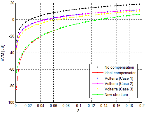
In Figure 10 we present EVM obtained for different compensator
structures, as well as output EVM with no compensation, and case with ideal compensator
. As can be seen from
Figure 10, compensator fitted using the proposed structure
in Figure 9
outperforms other compensators, and gives output EVM almost identical to the ideal
compensator. This result was to be expected, since model in
Figure 9 approximates the original system S
very closely, and thus is capable of approximating system
closely as well. This is not the case for compensators modeled with simple Volterra
series, due to inherently long (or more precisely infinite) memory introduced
by the LTI part of S. Even if we use noncausal Volterra series model
(i.e. ), which
is expected to capture true dynamics better, we are still unable to get good fitting
of the system S, and consequently of the compensator
.
Advantage of the proposed compensator structure is not only in better
compensation performance, but also in that it achieves better performance
with much more efficient strucuture. That is, we need far less
coefficients in order to represent nonlinear part of the compensator, in
both least squares optimization and actual implementation (Table 1).
In Table 1 we can see a comparison in the number of coefficients
between different compensator structures, for nonlinear subsystem parameter
value . Data in the first column is number of coefficients
(i.e. basis elements) needed for general Volterra model, i.e. coefficients
which are optimized by least squares. The second column shows actual number
of coefficients
used to build compensator. Least squares optimization yields many nonzero
coefficients, but only subset of those are considered
significant and thus used in actual compensator implementation.
Coefficient is considered significant if its value falls above
a certain treshold , where is chosen such that increase in EVM after zeroing
nonsignificant coefficients is not larger than 1% of the best achievable EVM
(i.e. when all basis elements are used for building compensator). From
Table 1 we can see that for case 3 Volterra structure, 10 times more
coefficients are needed in order to implement compensator,
than in the case of our proposed structure. And even when such a large number of
coefficients is used, its performance is still below the one achieved by this new
compensator model.
7 Conclusion
In this paper, we propose a novel explicit expression of the equivalent baseband model, under assumption that the passband nonlinearity can be described by a Volterra series model with the fixed degree and memory depth. This result suggests a new, non-obvious, analytically motivated structure of digital precompensation of passband nonlinear distortions caused by power amplifiers, in digital communication systems. It has been shown that the baseband equivalent model is a series connection of a fixed degree and short memory Volterra model, and a long memory discrete-time LTI system, called reconstruction filter. Frequency response of the reconstruction filter is shown to be smooth, hence well aproximable by low order polynomials. Parameters of such a model (and accordingly of the predistorter) can be obtained by applying simple least squares optimization to the input/output data measured from the system, thus implying low implementation complexity. State of the art implementations of DPD, have long memory requirements in the nonlinear subsystem, but structure of our baseband equivalent model suggests that the long memory requirements can be shifted from the nonlinear part to the LTI part, which consists of FIR filters and is easy to implement in digital circuits, giving it advantage of much lower complexity. We also argued that this baseband model, and its corresponding DPD structure, can be readily extended to OFDM modulation. Simulation results have shown that by using this new DPD structure, significant reduction in nonlinear distortion caused by the RF PA can be achieved, while utilizing full frequency band, and thus effectively using maximal input symbol rate.
Acknowledgment
The authors are grateful to Dr. Yehuda Avniel for bringing researchers from vastly different backgrounds to work together on the tasks that led to the writing of this paper.
References
- [1] P. B. Kennington, High linearity RF amplifier design. Norwood, MA: Artech House, 2000.
- [2] S. C. Cripps, Advanced techniques in RF power amplifier design. Norwood, MA: Artech House, 2002.
- [3] J. Vuolevi, and T. Rahkonen, Distortion in RF Power Amplifiers. Norwood, MA: Artech House, 2003.
- [4] A. A. M. Saleh, and J. Salz, ”Adaptive linearization of power amplifiers in digital radio systems,” Bell Syst. Tech. J., vol. 62, no. 4, pp. 1019-1033, April 1983.
- [5] W. Bösch, and G. Gatti, ”Measurement and simulation of memory effects in predistortion linearizers,” IEEE Trans. Microw. Theory Techn., vol. 37, pp. 1885-1890, December 1989.
- [6] J. Kim, and K. Konstantinou, ”Digital predistortion of wideband signals based on power amplifier model with memory,” Electron. Lett., vol 37, no. 23, pp. 1417-1418, November 2001.
- [7] L. Ding, G. T. Zhou, D. R. Morgan, Z. Ma, J. S. Kenney, J. Kim, and C. R. Giardina, ”A robust digital baseband predistorter constructed using memory polynomials,” IEEE Trans. Commun., vol. 52, no. 1, pp.159-165, January 2004.
- [8] V. J. Mathews and G. L. Sicuranza, Polynomial Signal Processing. New York: Wiley, 2000.
- [9] A. Zhu, and T. Brazil, ”Behavioral modeling of RF power amplifiers based on pruned Volterra series,” IEEE Microw. Wireless Compon. Lett., vol. 14, no. 12, pp. 563-565, December 2004
- [10] D. R. Morgan, Z. Ma, J. Kim, M. Zierdt, and J. Pastalan, ”A generalized memory polynomial model for digital predistortion of RF power amplifiers,” IEEE Trans. Signal Process., vol. 54, no. 10, pp. 3852-3860, October 2006.
- [11] A. Zhu, J. C. Pedro, and T. J. Brazil, ”Dynamic deviation reduction-based Volterra behavioral modeling of RF power amplifiers,” IEEE Trans. Microw. Theory Techn., vol. 54, No. 12, pp. 4323-4332., December 2006.
- [12] A. Zhu, P. J. Draxler, J. J. Yan, T. J. Brazil, D. F. Kimball, and P. M. Asbeck, ”Open-loop digital predistorter for RF power amplifiers using dynamic deviation reduction-based Volterra series,” IEEE Trans. Microw. Theory Techn., vol. 56, No. 7, pp. 1524-1534., July 2008.
- [13] M. Rawat, K. Rawat, and F. M. Ghannouchi, ”Adaptive digital predistortion of wireless power amplifiers/transmitters using dynamic real-valued focused time-delay line neural networks,” IEEE Trans. Microw. Theory Techn., vol. 58, No. 1, pp. 95-104, January 2010.
- [14] M. Rawat, K. Rawat, F. M. Ghannouchi, S. Bhattacharjee, and H. Leung, ”Generalized rational functions for reduced-complexity behavioral modeling and digital predistortion of broadband wireless transmitters,” IEEE Trans. Instrum. Meas., vol. 63, No. 2, pp. 485-498, February 2014.
- [15] C. Yu, L. Guan, and A. Zhu, ”Band-Limited Volterra Series-Based Digital Predistortion for Wideband RF Power Amplifiers,” IEEE Trans. Microw. Theory Techn., vol. 60, No. 12, pp. 4198-4208, December 2012.
- [16] O. Tanovic, R. Ma, and K. H. Teo, ”Novel Baseband Equivalent Models of Quadrature Modulated All-Digital Transmitters,” Radio Wireless Symposium (RWS) 2017, Phoenix, AZ, 15-17 Jan. 2017
- [17] G. M. Raz, and B. D. Van Veen, ”Baseband Volterra filters for implementing carrier based nonlinearities,” IEEE Trans. Signal Process., vol. 46, no. 1, pp. 103-114, January 1998.
- [18] M. Schetzen, The Volterra and Wiener theories of nonlinear systems. reprint ed. Malabar, FL: Krieger, 2006.
- [19] W. Frank, ”Sampling requirements for Volterra system identification,” IEEE Signal Process. Lett., vol. 3, no. 9, pp. 266-268, September 1996
- [20] J.Tsimbinos, and K.V.Lever, ”Input Nyquist sampling suffices to identify and compensate nonlinear systems,” IEEE Trans. Signal Process., vol. 46, no. 10, pp. 2833-2837, Oct. 1998.
- [21] J. G. Proakis and M. Salehi, Digital Communications. McGraw-Hill, 2007
- [22] D. C. Cox, ”Linear amplification with nonlinear components,” IEEE Trans. Commun., vol. 22, no. 12, pp. 1942-1945, Dec. 1974.
- [23] A. Goldsmith, Wireless Communications. Cambridge University Press, 2005.
- [24] S. H. Han and J. H. Lee, ”An overview of peak-to-average power ratio reduction techniques for multicarrier transmission,” IEEE Wireless Commun., vol. 52, pp. 5-65, March 2005
- [25] Q. Shi, ”OFDM in bandpass nonlinearity,” IEEE Trans. Consumer Electron., vol. 42, pp. 253-258, August 1996.
- [26] A. N. D’Andrea, V. Lottici, and R. Reggiannini, ”Nonlinear predistortion of OFDM signals over frequency-selective fading channels,” IEEE Trans. Commun., vol. 49, no. 5, pp. 837-843, May 2001.
- [27] F. Wang; D.F. Kimball, D.Y. Lie, P.M. Asbeck, and L. E. Larson, ”A Monolithic High-Efficiency 2.4-GHz 20-dBm SiGe BiCMOS Envelope-Tracking OFDM Power Amplifier,” IEEE J. Solid-State Circuits, vol.42, no.6, pp.1271,1281, June 2007.
- [28] J. Reina-Tosina, M. Allegue-Martinez, C. Crespo-Cadenas, C. Yu, and S. Cruces, ”Behavioral Modeling and Predistortion of Power Amplifiers Under Sparsity Hypothesis,” IEEE Trans. Microw. Theory Techn., vol. 63, no. 2, pp. 745-753, February 2015.
- [29] O. Tanovic, A. Megretski, Y. Li ,V. M. Stojanovic and M. Osqui, ”Discrete-time models resulting from dynamic continuous-time perturbations in phase-amplitude modulation-demodulation schemes,” 2016 IEEE 55th Conference on Decision and Control (CDC), Las Vegas, NV, 2016, pp. 6619-6624.