Can Tunnel Transistors Scale Below 10nm?
Abstract
The main promise of tunnel FETs (TFETs) is to enable supply voltage () scaling in conjunction with dimension scaling of transistors to reduce power consumption. However, reducing and channel length () typically deteriorates the ON- and OFF-state performance of TFETs, respectively. Accordingly, there is not yet any report of a high performance TFET with both low VDD (0.2V) and small (6nm). In this work, it is shown that scaling TFETs in general requires scaling down the bandgap and scaling up the effective mass for high performance. Quantitatively, a channel material with an optimized bandgap () and an engineered effective mass () makes both and scaling feasible with the scaling rule of for from 15nm to 6nm and corresponding from 0.5V to 0.2V.
Index Terms:
TFETs, nanowire, scaling, sub-10nm, direct tunneling, NEGF.I Introduction
Although tunnel FETs (TFETs) were originally proposed for low power applications [1, 2, 3], the low ON-current (ION) challenge in TFETs has concealed their scaling problem [4, 5, 6]. The low ION challenge can be solved by increasing the electric field at the tunnel junction; e.g. by using dielectric engineering [7], atomistically thin channels [8, 9, 10, 11], or internal polarization [12]. However, the scaling challenge is more tricky since the tunneling currents ION and IOFF depend on the same device parameters. Hence an attempt to decrease IOFF would reduce ION and vice versa. In contrast, ION and IOFF in MOSFETs are more independent of each other and a channel material with a large bandgap (or optimized effective mass) can be used for sub-12nm channels to suppress the direct source-to-drain tunneling [13, 14].
Fig. 1a shows the device structure of an InAs nanowire (NW) TFET with a diameter of 3.4nm. The transfer characteristics of the device simulated by the NEMO5 tool [25, 26, 27] are shown in Fig. 1b with IOFF fixed at 1. In the simulations, we scale down with the channel length (). The results indicate that the InAs NW-TFET exhibits a promising performance with long channel lengths (i.e. 9nm), however it completely fails to switch from OFF- to ON-state for the case of =6nm and =0.2V (i.e. ION/I).
Roughly, the transmission in the ON-state () and OFF-state () of TFETs depends on [15, 16]:
| (1) |
| (2) |
where and are the tunneling distances in the ON- and OFF-state (Fig. 1a) respectively. and are the reduced effective mass and the bandgap of the channel material.
The scaling of the channel below 10nm brings close to which reduces ION/IOFF significantly. One apparent solution can be a heterostructure channel where the term is different in (1) and (2) due to different materials used in those regions [12, 18]. However, it has been shown that the presence of band discontinuity and interface states in heterostructures can deteriorate the OFF-state performance of TFETs [19, 20]. Hence, in this work the homojunction TFETs have been considered as a more practical steep subthreshold swing () device.


On top of the length scaling problem which increases IOFF significantly, the voltage scaling reduces ION. The maximum tunneling window in TFETs approximately equals . Thus a short channel TFET with a small is expected to have a small ION/IOFF.
In this work, it is shown that by using a channel material with optimized and , it is still feasible to obtain an acceptable ION/IOFF for ultra-scaled TFETs (i.e. ION/I for =6nm and =0.2V). The solution to the scaling problem of TFET is to scale down of channel material to the smallest possible value to achieve a high ION. Of course cannot be smaller than , otherwise the channel cannot cover and block the tunneling energy window in the OFF-state. On the other hand, should scale up with scaling down the dimensions to decrease IOFF. Fig. 1c shows that the performance of 6nm long gate-all-around TFET can be improved more than 4 orders of magnitude by scaling down and scaling up . The favorable design space for and is discussed in Sec. IV.
II Simulation details
The self-consistent 3D Poisson-NEGF (Non-Equilibrium Green’s Function) method is used in the NEMO5 software for the simulation of InAs TFETs [25, 26, 27]. The InAs channel material is described by a 10 band nearest neighbor tight-binding model [28]. To find the impact of and on the performance of TFETs, a model is needed where and can be set as free input parameters, in contrast to the atomistic approach where and are the output of the simulation through material composition and geometry induced confinement effects. To reduce the number of free parameters, it is assumed that the electron and hole effective masses are equal (==). Recently, an analytical model was developed which produces results in excellent agreement with NEGF simulations [21]. To show the validity of this analytical model for ultra-scaled TFETs, the simulation results of scaled InAs TFETs with the scaling rule of obtained from the analytical model are benchmarked against the NEGF results first. Fig. 2 compares the results of analytical model and NEGF simulations. Notice that in Fig. 2, the OFF-state is not fixed unlike Fig. 1b. The accuracy and speed of the analytical model and tuneability of and makes this model an ideal tool for optimizing the TFET design.

III Simulation results
To analyze different TFET designs, the tunneling transmission path at the top of the tunneling window () is indicated as a function of source-channel tunneling window () in Fig. 3a. Knowledge of the tunneling transmission probability as a function of (i.e. ) provides information about the transfer characteristics [3]. Fig. 3b shows an example of with the corresponding TFET operational regimes (e.g. ON- and OFF-states, and n- and p- branches). Notice that is the ON-OFF transition point. For a small drain-source voltage, the I-V can be calculated by integrating the in the tunneling energy window (energies between and ). The tunneling transmission shows how far the TFET is from its ideal performance (i.e. and at OFF- and ON-state, respectively). Accordingly, ION, IOFF, and can be estimated from the maximum and minimum values of and its slope at subthreshold region. The impact of scaling on the transmission profile of InAs NW-TFET is shown in Fig. 3c. Reducing the channel length increases significantly while remains intact which was expected from equations (1) and (2).

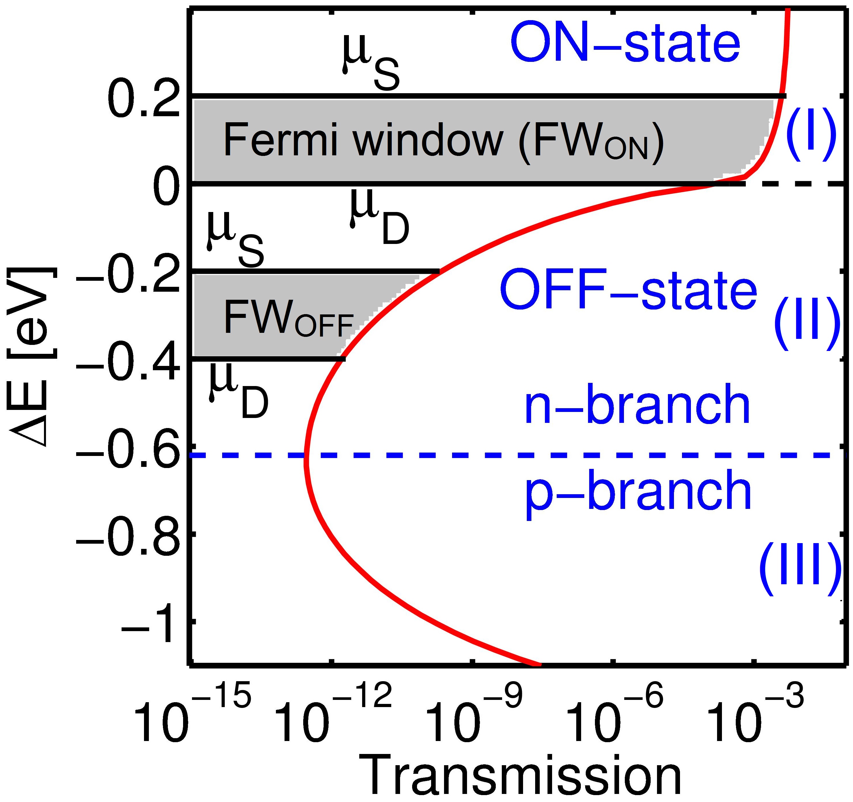


Fig. 3d shows the effect of bandgap on ; Obviously, a larger bandgap decreases both and . Notice that changing does not improve the subthreshold slope of (black lines in Fig. 3d). Increasing decreases more than since the prefactor of is larger for (note that in equations (1) and (2)). On the other hand, to reach this lower a larger gate voltage change is needed for larger band gaps (i.e. ). Thus, there is no noticeable improvement in with larger . On the other hand, increasing improves as shown in Fig. 3e. Since a larger does not require a larger gate voltage change, contrary to a larger . Fig. 3f compares TFETs with a constant but different ratios. Notice that not only improves with increasing ratio, but also . The reason for improved ON-state performance is that reducing decreases the depletion width at the source-channel interface and decreases in equation (1) [15].
IV Channel material with optimized properties
Fig. 4a shows the ION/IOFF ratio of NW-TFETs with =6nm and =0.2V and a channel material with different and . To suppress the p-branch of TFETs, the drain doping level is chosen to be much smaller than source doping level () and a gate leakage of 1 is assumed (I) [29]. The maximum ION/IOFF ratio is obtained with an of about . Moreover, with increasing , the optimum reduces and for the product (circle symbols) saturates (dashed line). Fig. 4b shows that TFETs with between and have acceptable ION/IOFF ratios according to ITRS requirements (ION/I).
Fig. 5a illustrates the favorable design space for as a function of for TFETs with the scaling rule of . The shaded area in Fig. 5a shows higher and lower bounds on and of the channel material for a high performance ultra-scaled NW-TFET.


Fig. 5b shows the transfer characteristics of NW-TFETs with optimized and from equations (3) and (4). ION/IOFF ratio of larger than and below 15 are obtained for all the cases including the 6nm long channel.


V Conclusion
In summary, the scaling of TFETs pushes the semiconductor industry to look for channel materials with higher , similar to ultra-scaled MOSFETs [13]. However, in TFETs channel material should have both and optimized. More accurately, the scaling of high performance NW-TFETs below 10nm requires:
- 1.
A channel material with scaled down band gap
(3) - 2.
A channel material with scaled up effective mass
(4) - 3.
Higher doping level in the source () than drain ().
(5) - 4.
A channel material with low dielectric constant () and a high-k oxide.
(6)
References
- [1] J. Appenzeller, Y.-M. Lin, J. Knoch, and Ph. Avouris, ”Band-to-band tunneling in carbon nanotube field-effect transistors,” Phys. Rev. Lett., vol. 93, no. 19, pp. 196805 (2004).
- [2] J. Appenzeller, Y.-M. Lin, J. Knoch, Z. Chen, and Ph. Avouris, ”Comparing carbon nanotube transistors-the ideal choice: a novel tunneling device design,” IEEE Trans. on Electron Dev. 52, 2568-2576 (2005).
- [3] A. M. Ionescu, and H. Riel, ”Tunnel field-effect transistors as energy-efficient electronic switches,” Nature, vol. 479, pp. 329–337 (2011).
- [4] U. E. Avci, and I. Young, ”Heterojunction TFET scaling and resonant-TFET for steep subthreshold slope at sub-9nm gate-length,” In IEEE International Electron Devices Meeting IEDM, pp. 4-3. (2013).
- [5] K. Boucart, and A. M. Ionescu, ”Length scaling of the double gate tunnel FET with a high-k gate dielectric,” Solid-State Electronics vol. 51, no. 11, pp. 1500-1507 (2007).
- [6] H. Lu, and A. Seabaugh, ”Tunnel Field-Effect transistors: state-of-the-art,” IEEE Electron Devices Society, vol. 2, no. 4, pp. 44-49 (2014).
- [7] H. Ilatikhameneh, T. Ameen, G. Klimeck, J. Appenzeller, and R. Rahman, ”Dielectric Engineered Tunnel Field-Effect Transistor,” IEEE Electron Device Letters (2015), 10.1109/LED.2015.2474147.
- [8] H. Ilatikhameneh, Y. Tan, B. Novakovic, G. Klimeck, R. Rahman, J. Appenzeller, ”Tunnel Field-Effect Transistors in 2D Transition Metal Dichalcogenide Materials,” IEEE Exploratory Solid-State Computational Devices and Circuits, vol. 1, no. 1, pp. 12-18 (2015), DOI: 10.1109/JXCDC.2015.2423096.
- [9] G. Fiori, F. Bonaccorso, G. Iannaccone, T. Palacios, D. Neumaier, A. Seabaugh, S. K. Banerjee, and L. Colombo, ”Electronics based on two-dimensional materials,” Nature nanotechnology, vol. 9, no. 10, pp. 768-779 (2014).
- [10] H. Ilatikhameneh, G. Klimeck, J. Appenzeller, and R. Rahman, ”Scaling Theory of Electrically Doped 2D Transistors,” IEEE Electron Device Letters, vol. 36, no. 7, pp. 726-728 (2015), DOI:10.1109/LED.2015.2436356.
- [11] Q. Zhang, G. Iannaccone, and G. Fiori. ”Two-Dimensional Tunnel Transistors Based on Thin Film.” IEEE Electron Device Letters, vol. 35, no. 1, pp. 129-131 (2014).
- [12] W. Li, S. Sharmin, H. Ilatikhameneh, R. Rahman, Y. Lu, J. Wang, X. Yan, A. Seabaugh, G. Klimeck, D. Jena, P. Fay, ”Polarization-Engineered III-Nitride Heterojunction Tunnel Field-Effect Transistors,” IEEE Exploratory Solid-State Computational Devices and Circuits, vol. 1, no. 1, pp. 28-34 (2015), DOI:10.1109/JXCDC.2015.2426433.
- [13] M. Salmani-Jelodar, S. Mehrotra, H. Ilatikhameneh, and G. Klimeck, ”Design Guidelines for Sub-12 nm Nanowire MOSFETs,” IEEE Trans. on Nanotechnology, vol. 14, no. 2, pp. 210-213 (2015).
- [14] K. Alam, and R. K. Lake, Monolayer MoS2 Transistors Beyond the Technology Road Map, IEEE Transactions on Electron Devices, 59.12, 3250 (2012).
- [15] H. Ilatikhameneh, R. B. Salazar, R. Rahman, G. Klimeck, J. Appenzeller, From Fowler-Nordheim to Non-Equilibrium Green’s Function Modeling of Tunneling, (2015) [Online.] http://arxiv.org/abs/1509.08170
- [16] E. O. Kane, ”Zener tunneling in semiconductors,” Journal of Physics and Chemistry of Solids, vol. 12, no. 2, pp. 181-188 (1960).
- [17] H. Iwai, ”Roadmap for 22nm and beyond,” Microelectronic Engineering vol. 86, no. 7, pp. 1520-1528 (2009).
- [18] T. Krishnamohan, D. Kim, S. Raghunathan, and K. Saraswat. ”Double-Gate Strained-Ge Heterostructure Tunneling FET (TFET) With record high drive currents and subthreshold slope ¡¡ 60mV/dec,” In IEEE International Electron Devices Meeting IEDM, pp. 1-3 (2008).
- [19] J. Knoch, and J. Appenzeller. ”Modeling of high-performance p-type III–V heterojunction tunnel FETs,” IEEE Electron Device Letters, vol. 31, no. 4, pp. 305-307 (2010).
- [20] S.O. Koswatta, S.J. Koester, and W. Haensch, ”On the possibility of obtaining MOSFET-like performance and sub-60-mV/dec swing in 1-D broken-gap tunnel transistors,” IEEE Trans. Electron Devices 57, 3222 (2010).
- [21] R. B. Salazar, H. Ilatikhameneh, R. Rahman, G. Klimeck, J. Appenzeller, ”A New Compact Model For High-Performance Tunneling-Field Effect Transistors,” [Online]. http://arxiv.org/abs/1506.00077
- [22] J. R. Williams, L. DiCarlo, and C. M. Marcus, ”Quantum Hall effect in a gate-controlled pn junction of graphene,” Science, vol. 317, pp. 638-641 (2007).
- [23] J. F. Tian, L. A. Jauregui, G. Lopez, H. Cao, and Y. P. Chen, ”Ambipolar graphene field effect transistors by local metal side gates,” Applied Physics Letters, vol. 96, no. 26, pp. 263110 (2010).
- [24] S. Agarwal, and E. Yablonovitch, ”Band-Edge Steepness Obtained From Esaki/Backward Diode Current–Voltage Characteristics,” IEEE Transaction on Electron Devices, vol. 61, no. 5, pp. 1488-1493 (2014).
- [25] J. E. Fonseca, T. Kubis, M. Povolotskyi, B. Novakovic, A. Ajoy, G. Hegde, H. Ilatikhameneh, Z. Jiang, P. Sengupta, Y. Tan, G. Klimeck, ”Efficient and realistic device modeling from atomic detail to the nanoscale,” Journal of Computational Electronics, vol. 12, no. 4, pp. 592-600 (2013).
- [26] S. Steiger, M. Povolotskyi, H. H. Park, T. Kubis, and G. Klimeck, ”NEMO5: a parallel multiscale nanoelectronics modeling tool,” IEEE Transaction on Nanotechnology, vol. 10, no. 6, pp. 1464-1474 (2011).
- [27] J. Sellier, et al., ”Nemo5, a parallel, multiscale, multiphysics nanoelectronics modeling tool,” SISPAD, (2012).
- [28] T.B. Boykin, G. Klimeck, R.C. Bowen, and F. Oyafuso, Diagonal parameter shifts due to nearest-neighbor displacements in empirical tight-binding theory Phys. Rev. B 66, 125207 (2002).
- [29] M. Salmani-Jelodar, H. Ilatikhameneh, S. Kim, K. Ng, and G. Klimeck, ”Optimum High-k Oxide for the Best Performance of Ultra-scaled Double-Gate MOSFETs,” (2015), [Online.] arXiv:1502.06178.